❌

Reading view

China cuts photonic chip costs by 90% using nanoscale stamping on eight-inch wafers
A Chinese startup has claimed a breakthrough in photonic chip manufacturing by producing 8-inch optical chip wafers without relying on conventional deep ultraviolet (DUV) lithography systems.

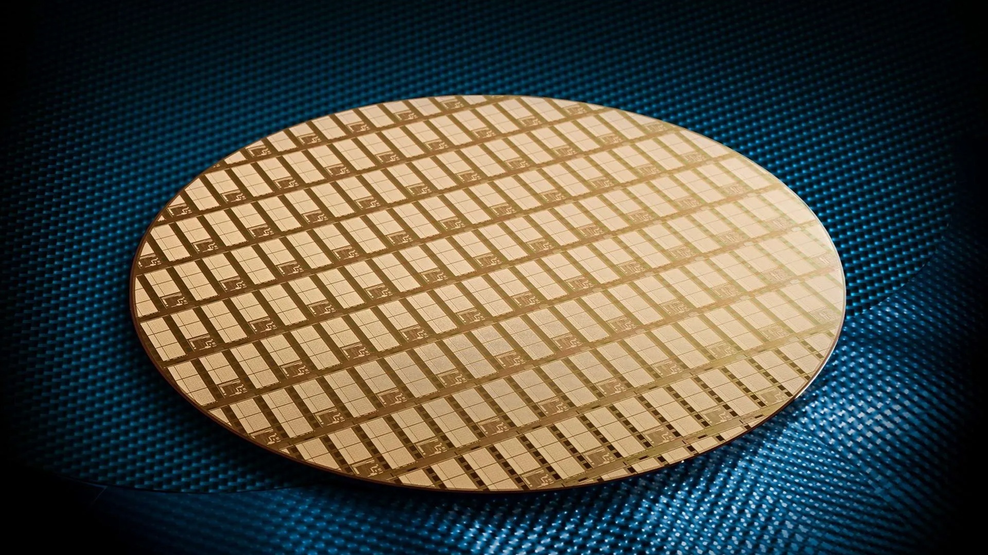
Hangzhou-based Prinano said it successfully validated mass production of photonic chips using its nanoimprint lithography (NIL) technology, a manufacturing approach that physically stamps nanoscale patterns onto wafers instead of projecting them through optical systems.

According to the company, the process was carried out in collaboration with Shenzhen Litra Technology and used its PL-AS vacuum air-cushion nanoimprint lithography equipment. Prinano said the method “completely avoids” the need for DUV lithography tools while reducing manufacturing costs to about one-tenth of traditional solutions.

The announcement comes as Chinese chipmakers continue looking for alternative manufacturing technologies amid restrictions on access to advanced lithography systems from Dutch supplier ASML.

Seeking lithography alternatives

Photonic chips are used in applications such as optical communications, sensing systems, lidar, and data centers. Unlike conventional electronic chips, they process information using light rather than electrical signals.

Prinano said its technology supports wafer-level production of photonic chips and can be applied to optical communication and sensing devices based on gallium arsenide, indium phosphide, and silicon photonics.

The company said its PL-AS tool offers sub-10-nanometer line-width resolution along with wafer-level pressure control. However, it did not disclose production volumes, manufacturing yields, or customer shipment data.

Nanoimprint lithography has long been viewed as a potential alternative to traditional optical lithography because it can create extremely fine features without the need for expensive projection optics. The technology was pioneered in the 1990s by Princeton University professor Stephen Y. Chou.

Prinano founder Ge Haixiong studied under Chou and established the company in 2017 to develop NIL equipment, materials, and manufacturing processes.

Questions over scalability

Interest in nanoimprint lithography has increased in recent years as chipmakers seek lower-cost manufacturing methods. In 2023, Canon introduced a commercial NIL system and promoted it as an alternative to some advanced lithography tools.

Despite the promise, analysts have questioned whether the technology can match the throughput and yields required for large-scale semiconductor manufacturing.

Research firm SemiAnalysis has previously noted that while NIL equipment can be cheaper than advanced lithography tools, overall economics depend on factors such as defect rates, template production, throughput, and process integration.

Prinano’s announcement focuses specifically on photonic chips rather than advanced logic processors, a distinction that may make commercialization more achievable. Photonic devices often rely on repeating nanoscale structures such as gratings, waveguides, and ring resonators, which can be well suited to imprint-based manufacturing.

The company said the technology has moved into wafer-level production validation, but independent verification of yields, commercial deployment, and manufacturing scale has not yet been disclosed.

For China’s semiconductor industry, the development highlights ongoing efforts to explore alternative manufacturing routes as access to advanced lithography equipment remains restricted.

  •  

MIT’s cooling tech allows data centers to extract 35% more tokens with same power

Ferveret, a startup from the Massachusetts Institute of Technology (MIT), is using cooling technology deployed in nuclear reactors to solve challenges faced by data centers today. The waterless cooling technology can also help establish data centers in areas where water is scarce while abundant solar energy powers the chips and cooling infrastructure. 

The recent surge in artificial intelligence (AI) applications has been made possible by high-performance computing chips from companies like NVIDIA. When AI needs to be deployed at scale, companies need to house many chips capable of processing information quickly enough. To save costs, they hire computing power from private data centers that buy and deploy the high-performance chips and rent them out over the long term. 

As more and more companies deploy AI in their workflows, the demand for data centers has shot up. With new data centers, energy demand is also growing. Estimates suggest that by the end of the decade, up to 17 percent of the US electricity usage will be consumed by data centers. The power consumption is not just for high-performance chips but also for cooling them. 

Liquid cooling chips

When data centers were first set up, chips were cooled using air. As their computing capacities increased, they began to generate more heat, which needed better cooling approaches. 

Liquids are better than air at removing heat from a chip. Their performance is even better when the heat is used to bring about a phase change. At the liquid’s boiling point, it can extract more heat from the chip without increasing the temperature difference between the liquid and the chip. 

The newest data centers use an immersion cooling approach in which the entire server rack is immersed in the cooling liquid to maximize heat transfer. However, with AI adding more computational power to the server pack, heat generation has increased, necessitating newer cooling solutions. 

Nuclear reactor-inspired tech

MIT spin-off Ferveret is looking to deploy cooling technology used in nuclear reactors and adapt it for data center use. Called subcooled boiling, it uses a liquid with a low boiling point, which produces smaller bubbles than immersion cooling approaches. 

While immersion cooling has to contend with issues such as capturing the bubbles and reliquefying them under constrained pressure and temperature conditions, in Ferveret’s approach, the bubbles recondense quickly into the surrounding liquid. 

In a recent study, Ferveret found that its cooling solution resulted in up to 15 percent improvement in computational power efficiency compared to state-of-the-art immersive cooling techniques. This, combined with Fereveret’s proprietary power control system, allows data centers to extract 35 percent more tokens from the AI models without any increase in power usage. 

Ferveret’s Adaptive Phase Cooling (APC) system is deployed in small boxes, each capable of housing one server. This modular approach allows its deploy and maintain its system much more easily. 

“The physics enable us to get to form factors that weren’t possible in the past,” said Reza Azizian, co-founder at Ferveret, in a press release. “Most immersion cooling solutions are large tanks that people submerge the servers in. We have a smaller, modular rack-mounted solution that makes it adaptable to the current infrastructure, so it’s easier for people to deploy our technology.”

The waterless cooling approach is also beneficial in areas where water is scarce, but sunlight is plentiful. Setting up solar power plants in these areas is simple, but with low water, data centers could not be cooled down. 

“This technology can help deploy data centers in regions where normally you wouldn’t have the resources to do so, including Africa, the Middle East, and of course parts of America. It’s a huge unlock,” added Matteo Bucci, associate professor at the Department of Nuclear Science and Engineering and also Ferveret co-founder. 

  •  

Europe debuts first end-to-end sovereign manufacturing flow for critical defense chips

Europe’s effort to strengthen control over its semiconductor supply chain has reached a significant milestone. GlobalFoundries and Dutch chip designer Qualinx have completed what they describe as the continent’s first fully European end-to-end semiconductor manufacturing flow.

The achievement shows that security-sensitive chips can move from design to fabrication entirely within Europe. The approach targets applications where supply chain control carries strategic importance, including aerospace, defense, and critical infrastructure.

Qualinx served as the first customer to validate the manufacturing process using one of its advanced satellite navigation chips designed for secure timing and positioning applications.

Securing the supply chain

The project centers on Qualinx’s QLX3xx Global Navigation Satellite System system-on-chip, developed for Positioning, Navigation and Timing applications. These technologies support systems that require precise synchronization and resilient navigation capabilities.

Potential uses include military platforms, critical communications networks, and ultra-low-power connected devices operating at the edge. The chip was manufactured using GlobalFoundries’ FDX platform at the company’s Dresden facility in Germany.

Under the manufacturing framework, sensitive design files and production materials remain within European borders throughout the process. The initiative also receives support through the European Chips Act, which seeks to strengthen the region’s semiconductor capabilities and reduce reliance on overseas suppliers.

“We are demonstrating that Europe can rely on a secure, end-to-end semiconductor manufacturing flow that meets the highest requirements of aerospace and defense,” said Dr. Manfred Horstmann, senior vice president and general manager at GlobalFoundries.

He added that the Qualinx project proves complex, security-focused chip designs can already enter production through a trusted European manufacturing route.

Sovereign production roadmap

GlobalFoundries plans to expand the capability over the next several years. The Qualinx tape-out represents the first operational step toward a fully automated sovereign manufacturing process.

The company expects to complete that transition in Dresden by the end of 2026. Beginning in 2027, aerospace, defense and critical infrastructure customers could access the manufacturing flow through standard foundry engagements.

GlobalFoundries also plans to incorporate additional European partners into the ecosystem, including intellectual property providers, mask houses, and outsourced semiconductor assembly and test companies.

According to the company, several European system manufacturers and infrastructure operators have already begun evaluating future products for the trusted manufacturing path. The successful Qualinx project could help lower both technical and regulatory barriers for follow-on programs.

Building trusted infrastructure

The effort extends beyond wafer fabrication and chip production. GlobalFoundries is also working with European telecommunications and cloud providers to keep production data within the region.

In a separate initiative with Deutsche Telekom, the company is examining how manufacturing information can travel through European networks and reside in European data centers. The work covers encryption practices, secure data routing, and access controls for highly sensitive workloads.

For Qualinx, the project validates both its technology and the broader concept of sovereign semiconductor production.

“This first secure product demonstrates that a fully European manufacturing path is already a reality today,” said Tom Trill, chief executive officer of Qualinx.

He said the collaboration optimized the company’s Digital RF technology on GlobalFoundries’ FDX platform while preserving control over intellectual property, data, and the supply chain.

As governments around the world seek greater control over strategic technologies, Europe’s latest semiconductor milestone suggests trusted regional manufacturing is evolving beyond policy ambitions. It is increasingly becoming an industrial reality.

  •  

Next-gen wireless drone swarm stays airborne 24/7, never needs to land

US firms Reach Power and Gambit have announced their joint SWARM project has received funding from the Department of War’s Operational Energy Capability Improvement Fund (OECIF).

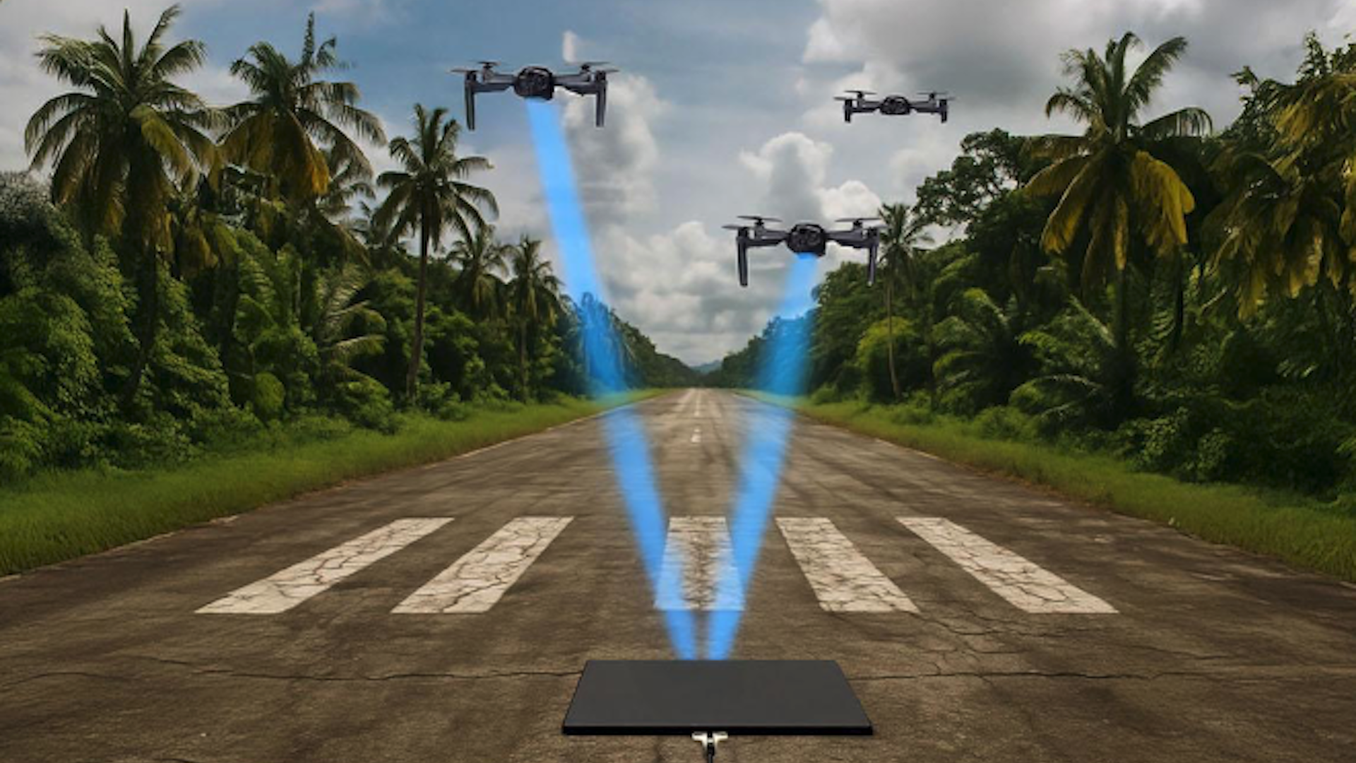
The new project combines wireless power beaming with AI-driven swarm intelligence to enable small drone fleets that operate on a constant basis without needing to land or swap batteries.

According to the teams behind the project, it untethers drones from the limitations of limited battery charges, removing the need to manually swap batteries. This will enable 24/7 air time, allowing uninterrupted operations.

A next-gen drone swarm

Group 1 drones, the small and inexpensive uncrewed systems widely used in modern conflicts, typically fly for only about 30 minutes on a single battery charge.

Once a swarm launches and organizes, effective mission time shrinks even further. According to a Reach press statement, larger batteries increase cost and weight, undermining the key benefit of drones—the fact that they are low-cost, expendable assets.

The logistics of large drone fleets is complex and often cost-prohibitive. Operators must install, remove, charge, and swap batteries for each drone before and after every flight. In contested areas, resupply becomes hazardous and contributes to reported drone effectiveness rates as low as 30 percent in active combat.

SWARM aims to tackle these constraints by integrating Reach Power’s wireless power-beaming technology with Gambit’s autonomous systems software.

Drones fly to designated waypoints to receive targeted radio-frequency (RF) energy mid-mission without landing or human assistance.

Gambit’s AI allows each aircraft to monitor its battery level, mission requirements, and charging opportunities, then adjust routes and behaviors in real time. The combined system lets the swarm self-manage energy distribution, maintain continuous presence, and reduce reliance on ground support.

Unlocking the ‘full potential of autonomy’

Chris Davlantes, founder and CEO of Reach Power, emphasized the importance of finding solutions to the limits of battery-operated fleets.

“Drone swarms are only as persistent as their batteries. SWARM changes the equation,” he noted. “When a drone can recharge itself in the air without human intervention, the full potential of autonomy and swarming is unleashed from battery limits.”

Josh Giegel, CEO of Gambit, meanwhile, highlighted the operational impact the new system could have for modern drone operations. “Today’s limitation isn’t just endurance, it’s the operational burden that comes with it,” he said.

“By enabling systems to manage energy and coordinate behavior autonomously, SWARM allows operators to focus on the mission instead of sustaining the systems.”

The SWARM project targets missions that require sustained coverage, including intelligence, surveillance, and reconnaissance (ISR), counter-uncrewed aircraft systems (c-UAS), border security, air defense, and force protection.

Reach Power develops RF-based wireless charging solutions for drones, sensors, and robots that eliminate cables and battery logistics across defense and industrial sectors. Gambit, meanwhile, provides AI software for coordinated, adaptive behavior in heterogeneous robotic teams operating in complex environments.

OECIF serves as the US Department of War’s primary program for investing in operational energy innovations, with power beaming listed as a priority under demand-reduction efforts. The SWARM award reflects growing military interest in technologies that extend small-drone endurance while lowering logistical risks.

“OECIF’s early investment in power beaming is yielding significant strategic dividends as the battlefield shifts toward autonomous operations,” said Christopher DePuma, Operational Energy and Power Projection Portfolio Lead.

“By enabling remote sensors and drones to maintain persistent ISR, this technology unlocks their true potential—eliminating the tether of battery swaps and constant recharging to provide an unblinking eye on the target.”

  •  

VivaTech ouvre ses portes à 10 000 future makers et à l'avenir

Avec « 10 000 Future Makers » et en partenariat avec Futura, VivaTech affirme sa volonté de préparer la relève de l’écosystème technologique européen en connectant les jeunes générations aux grands enjeux de l’innovation, de la transition numérique et de l’entrepreneuriat.

  •  

MIT’s new imaging tech delivers sharp 3D images in murky waters up to 65 feet away

A team of engineers at the Massachusetts Institute of Technology (MIT) has developed a groundbreaking imaging system capable of capturing detailed 3D images through even the murkiest waters.

The new technology, which harnesses the power of single-photon detectors and advanced computational algorithms, is poised to significantly enhance underwater exploration, search-and-rescue operations, and environmental monitoring.

Breakthrough in underwater imaging

Traditional methods for underwater imaging, such as sonar and optical cameras, have struggled to provide clear visuals in turbid environments. Particles in the water scatter light, making it nearly impossible to see beyond a few meters (about 6.5 feet) in highly cloudy conditions.

However, the new MIT system can generate sharp, three-dimensional images from distances up to 20 meters (about 65.6 feet) in water with extremely high turbidity.

How the technology works

At the core of the system is a pulsed laser that emits bursts of light into the water. As these pulses bounce off objects and return, they are detected by a highly sensitive single-photon avalanche diode (SPAD) array.

Each photon’s journey is recorded, allowing the system to calculate the precise distance and shape of submerged objects, even when only a handful of photons make it back through swirling sediment.

To interpret the faint signals, the team developed new computational algorithms that reconstruct 3D scenes from the sparse, scattered data. The result: detailed images that would be impossible for conventional cameras to achieve in similar conditions.

Potential applications and future impact

According to the MIT team, this imaging breakthrough could revolutionize a range of underwater activities. Search and rescue teams could locate lost objects or people more quickly in cloudy lakes or coastal waters. Marine biologists could study habitats previously hidden by sediment. Archaeologists might uncover ancient shipwrecks buried beneath layers of silt.

The technology could also be invaluable for inspecting underwater infrastructure, such as pipelines, bridges, or dams, where safety and clarity are paramount.

Testing and results

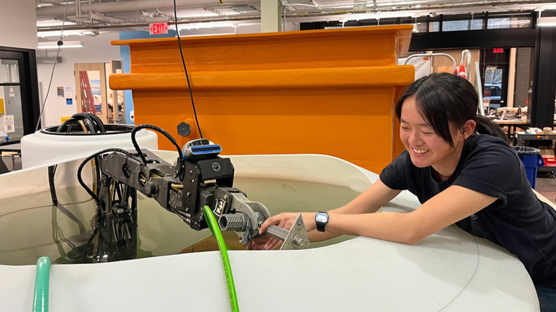
The research team tested their prototype in a specially designed tank filled with water so murky that standard cameras could not see beyond 3 centimeters (about 1.2 inches). With their new system, they successfully imaged objects at distances up to 20 meters (65.6 feet), a feat previously thought unattainable in such conditions.

The system is also energy efficient, requiring less power than traditional active imaging methods, and can be made compact enough for use on underwater drones or remotely operated vehicles.

Looking ahead

While the current prototype is a significant leap forward, the researchers are already working to refine the technology, aiming to increase imaging speed and resolution. They envision future versions integrated into autonomous underwater vehicles for continuous monitoring of oceans, lakes, and rivers.

MIT’s new imaging system represents a major advance in overcoming the challenges of underwater visibility and could open up a new era of aquatic discovery and safety.

  •  

US could soon detect missile, meteorite composition analyzing impact flashes

Researchers in the United States are studying impact flashes generated by high-speed collisions. It’s being claimed that advances in understanding the optical impact flashes can be highly beneficial for missile defense, making it possible to determine the composition of an intercepted missile and its payload.

Conducted by researchers in Southwest Research Institute (SwRI), the work could also aid scientists in identifying the origins of meteorites or asteroids impacting surfaces, based on their composition.

Energy of the impact creates a flash

“When a meteorite strikes the surface of a moon or planet, the energy of the impact creates a flash that gives off so much energy that the chemical signatures of its constituent materials are visible at different wavelengths,” said Dr. Pablo Bueno, a lead engineer in SwRI’s Mechanical Engineering Division.

Researchers have revealed that the impact flash is a physical phenomenon resulting from conventional and hypervelocity impact. The emission of the flash is related to the composition of the target; thus, spectrographic measurements provide spectral data that could be used to identify the materials involved in the collision, according to the project.

Bueno and Roberto Enriquez-Vargas, an SwRI senior research engineer, recently completed an internally funded SwRI project that developed and refined methods for using high-speed spectroscopy to analyze the light emitted during hypervelocity impacts, where the impact flashes typically only last a few microseconds. The short time window required capturing spectral data quickly and precisely, according to a press release.

Laser-based triggering system

Bueno and Enriquez-Vargas used both of SwRI’s two-stage light-gas guns to create hypervelocity impacts representative of missile strikes or asteroid impacts. The large gun system generates velocities up to 7 kilometers per second (15,660 mph). The system is 22 meters (72 feet) long and traditionally used to study ballistics, as per the release.

Because the impact occurs so swiftly and the flash decays rapidly, Bueno and Enriquez-Vargas developed a laser-based triggering system to precisely detect the instant an impact occurs, accurately measuring impact timing within 100 nanoseconds, or one 10-millionth of a second, according to researchers.

“Thicker targets produced brighter, longer flashes,” Bueno explained. “Higher atmospheric pressure created broader and thicker emission lines in the spectra, and in many cases materials at high temperature behaved differently than they did when impacted at room temperature.”

The team developed and tested laser-based triggering scheme. Accurate timing within 100 ns of the impact was demonstrated.

The team also revealed that the strong lines of the emission spectra of aluminum and copper have been measured and characterized within ±2 nm of their published values. The doublet near 396 nm, for aluminum, and the triple near 515 nm, for copper, have been selected as the best lines to continue with the experimental test matrix.

The effects of projectile flight speed, atmospheric pressure, and atmospheric composition have been documented. These results are fulfilled in part metric 3 of the program. The results show these parameters affect the amplitude and width of the emission lines, according to the project.


  •  
❌