
❌

Reading view

“Magic-Angle” Graphene Uses Faint Light to Transform an Insulator Into a Metal, Revealing a New Way to Make the Unseen Visible

A material that normally blocks the flow of electricity can suddenly begin behaving like a metal when exposed to remarkably weak light, according to a new experiment involving one of the strangest forms of graphene ever created. The breakthrough reveals that an unusual quantum effect could eventually provide a new way to detect some of the faintest radiation around us.

Researchers working with “magic-angle” twisted bilayer graphene found that faint, long-wavelength radiation can effectively melt the material’s fragile correlated insulating state, causing its electrical resistance to plummet. Remarkably, the experiments showed that even relatively weak radiation could trigger a dramatic transition from an insulator to a metal.

Beyond revealing an unusual way that light can manipulate matter, the discovery could provide the foundation for extremely sensitive detectors capable of spotting faint terahertz and far-infrared radiation.

With further development, detectors operating at these wavelengths could have applications ranging from security imaging and material inspection to astronomy and environmental sensing.

The study, published in Nature Communications, centers on magic-angle twisted bilayer graphene, or MATBG—a material produced by stacking two sheets of graphene and rotating them relative to one another at a carefully controlled angle.

Under the right conditions, interactions between electrons can cause magic-angle graphene to enter exotic collective states, including superconducting and insulating phases.

“Here we show that this expectation does not apply to magic-angle twisted bilayer graphene (MATBG) and demonstrate giant photoresponse of MATBG to low-intensity long-wavelength photons when it is tuned to half filling of the moiré band,” researchers write. “Far-infrared photons selectively overheat the low-heat-capacity electronic subsystem, driving a collapse of the correlated order and producing a giant photoresistive response.”

Ordinarily, changing an insulator into a conductor with light requires supplying enough energy to alter how electrons can move through the material fundamentally. Previous experiments involving light-induced insulator-to-metal transitions have frequently depended on intense, ultrafast excitation.

Magic-angle graphene offers another route.

Twisting graphene sheets at carefully controlled angles creates a larger repeating structure known as a moiré superlattice, dramatically changing how electrons within the material interact. Those interactions have already produced some remarkable results.

As The Debrief reported last year, researchers studying magic-angle twisted trilayer graphene uncovered new evidence of unconventional superconductivity, including unusually tightly bound electron pairs and a distinctive superconducting energy gap.

That work was part of a greater effort to understand whether these exotic materials could eventually help scientists design superconductors capable of operating at much higher temperatures.

In the new study, researchers exploited another unusual state that can emerge in magic-angle graphene. At certain electron densities, interactions between electrons become unusually important, allowing them to organize into what physicists call a “correlated insulator.”

That collective state is extremely fragile. The correlated insulating gap exists at an energy scale of only a few millielectronvolts. Previous measurements cited by the researchers indicate that a gap of approximately 1 millielectronvolt at very low temperatures gradually closes as the material warms and disappears around 10 kelvin.

The researchers realized that weakness could become an advantage.

Their experimental device consisted of magic-angle graphene sandwiched between layers of hexagonal boron nitride and configured as a field-effect transistor. A graphite back gate allowed them to precisely control the number of charge carriers and tune the graphene into its correlated insulating state.

They then exposed it to millimeter-wave and far-infrared radiation.

Instead of needing to inject large numbers of charge carriers, the incoming photons heated the graphene’s low-heat-capacity electronic system. That relatively small temperature increase was enough to destabilize the cooperative electronic order, retaining the insulating state.

The gap collapsed, resistance dropped dramatically, and the material became metallic.

Measurements in darkness and under illumination reinforced that interpretation. Without radiation, the graphene displayed the temperature-sensitive resistance expected from an insulator. Under millimeter-wave illumination, it instead exhibited behavior representative of a metal.

Researchers compare the mechanism to superconducting bolometers, highly sensitive radiation detectors in which incoming energy interrupts a superconducting state. But their graphene device essentially operates in reverse: instead of destroying a zero-resistance state, approaching photons destroy a high-resistance correlated insulating state and turn it metallic.

That makes the insulator-to-metal transition more than an unusual demonstration of quantum physics. It becomes the detector’s signal.

The team found that the device responded across wavelengths ranging from 85 to 2,140 micrometers, encompassing far-infrared and millimeter-wave radiation.

That portion of the electromagnetic spectrum is particularly interesting because it can reveal things ordinary cameras cannot. Terahertz radiation can penetrate some materials opaque to visible light, while interactions between this radiation and matter can provide information about a material’s composition.

More capable detectors could therefore eventually contribute to technologies such as security scanners looking for concealed objects, systems inspecting manufactured components without cutting them open, or sensors identifying substances using characteristic spectral markers.

Astronomy offers another potential application. Cold dust, star-forming regions, and other objects that may be faint or obscured at visible wavelengths emit radiation in the far-infrared. Detecting those extremely weak signals requires exceptionally sensitive instruments, making improved detector technology valuable for future astronomical observatories.

The experimental graphene detector exhibited considerable intrinsic sensitivity. The researchers measured an internal voltage responsivity of approximately 17 million volts per watt of absorbed power. They note that its internal responsivity exceeds that of many commercial bolometers operating in the same spectral region.

However, researchers caution that practical external performance is presently limited partly by how efficiently radiation is absorbed, meaning the experimental device is not equivalent to a finished commercial detector. Better antennas, cavities, metamaterials, or other structures designed to funnel radiation into the graphene could potentially improve its performance considerably.

There are other hurdles. The effect currently requires ultra-low temperatures, and the unusually strong response depends upon generating high-quality magic-angle graphene structures. Those requirements mean practical security scanners or telescope cameras based on the technology remain prospective rather than imminent.

Still, there are encouraging characteristics. The photoresponse persisted at temperatures around 6 to 7 kelvin and remained robust in magnetic fields of several tesla, with substantial reduction appearing only above roughly 4 tesla. That magnetic-field tolerance could make the technology attractive for specialized scientific instruments where superconducting detectors may meet limitations.

The current device also has an estimated practical response time of roughly 50 nanoseconds, largely because of its electrical design. The underlying electron cooling occurs much faster, and researchers estimate that smaller devices could reduce that practical limit by at least an order of magnitude. They also envision twisted multilayer materials, wafer-scale growth, and large-format detector arrays as potential directions for future development.

For now, the experiment demonstrates that in certain quantum materials, changing electrical behavior does not necessarily require pumping large amounts of energy into individual electrons. Sometimes, a small amount of light only needs to destabilize the collective state that those electrons have constructed together.

For physicists, the discovery offers a new way to investigate how fragile collective states of matter collapse and recover. For engineers, that same fragility could become useful precisely because extraordinarily weak radiation can trigger an extraordinarily large electrical response.

“Our experiments can be further generalized for time-domain interrogation of the CI state itself,” researchers write. “Radiation-driven excitation confined within the flat band, combined with time-resolved monitoring of the CI photoresistance, would allow direct access to the intrinsic timescale of correlated-order suppression and recovery, thereby probing the collective dynamics within the ground state.”

Study: Elesin, L., Shilov, A. L., Kravtsov, M. et al. “Correlated Insulator Moiré Bolometer.” Nature Communications (2026).

Tim McMillan is a retired law enforcement executive, investigative reporter and co-founder of The Debrief. His writing typically focuses on defense, national security, the Intelligence Community and topics related to psychology. You can follow Tim on Twitter: @LtTimMcMillan.  Tim can be reached by email: tim@thedebrief.org or through encrypted email: LtTimMcMillan@protonmail.com 
  •  

Metasurface grating gives solar telescopes a boost

A compact optical technology that has already proved its worth in Earth-bound applications could be on its way to space after researchers at the University of California San Diego, US showed that it can map the Sun’s magnetic field just as well as traditional instruments. By making polarization gratings from specially engineered metasurfaces rather than a complex assembly of optics, the researchers say that future solar-observing missions could benefit from reduced complexity and cost as well as size.

“Our work makes use of recent advancements in nanoscale optical technologies to help improve the hardware for making astronomical observations of the Sun,” says study leader Noah Rubin of UC San Diego’s Jacobs School of Engineering. “We believe this is one of the first times that metasurface optics – which have been a subject of intense interest in both academic research and industry for about a decade – have been used to improve scientific instrumentation of any kind outside of a lab/academic proof-of-concept.”

Polarized light and solar magnetic fields

Although light emitted by the Sun is generally unpolarized – that is, the light waves do not vibrate along a particular axis – strong magnetic fields that develop near sunspots can polarize this light via the quantum mechanical Zeeman effect. These magnetic fields are closely associated with space weather events such as solar storms that can damage electronic infrastructure both on Earth and in orbit. Studying the Sun’s magnetic activity by monitoring areas of polarized light is thus an important step towards detecting or predicting such storms in time to take protective action.

Usually, measuring the polarization state of light means analysing different polarization directions using a device such as a waveplate that mechanically rotates between exposures. Rubin compares this process to taking several photographs through polarized sunglasses held at different angles, then combining them to obtain a fuller picture of what’s going on.

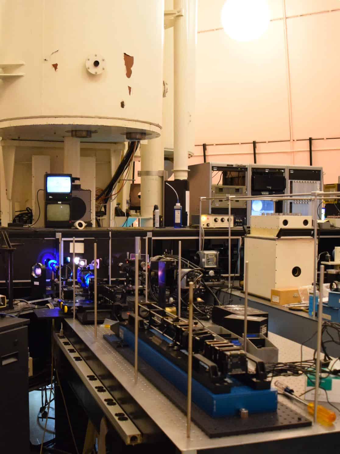
Photo of the custom-built telescope being tested at the Dunn Solar Telescope
Test rig: Sunlight from the top of the Dunn Solar Telescope’s 136-foot-tall tower travels 228 feet underground and is reflected back up to this room at ground level, where it passes through an optical system (blue lights, background) before reaching the team’s custom-built telescope (foreground). (Courtesy: Noah Rubin)

While this technique works, and instruments that use it have already been sent into space, the image analysis process is very time-consuming. It also requires an external power source, and the need to mechanically rotate the waveplate introduces extra complexity and cost, says Rubin.

“In space-based applications, a satellite itself can be moving while this component reorients, causing a highly undesirable blurring effect,” he explains. “As a result, designers of these systems often invest considerable resources into mechanical remediation and engineering to correct the motion of the telescope on the satellite, and this frequently ends up being substantially more expensive than the telescope optics themselves.”

A metasurface solution

In the new study, which is detailed in Science Advances, Rubin and colleagues solved this problem by creating a polarization-sensitive metasurface that splits light into its different polarization components. A camera-like system containing this metasurface polarization grating can then form multiple images of a scene in parallel. Rubin explains that each image in this scene is analysed with respect to a different polarization state, meaning that the system can measure the polarization of light simultaneously and passively in a single camera frame.

Rubin notes that this technique of condensing an instrument that would ordinarily involve a complex assembly of optics into a single, flat surface has previously made its way into applications as diverse as facial recognition in mobile phones and the preparation of complex photon states in quantum optics experiments. “In this work, we show that these advantages translate to polarization imaging in astronomy,” he tells Physics World.

Comparable results

Working with industrial partners at BAE Systems Space & Mission Systems in Colorado, US (formerly known as Ball Aerospace, which Rubin describes as “well-known for its involvement in the development of the James Webb Space Telescope, Hubble and countless other NASA missions”), the team designed a specialized telescope built around such a metasurface polarization grating. They also deployed their instrument on the Dunn Solar Telescope in New Mexico, US, and showed that they could quantitatively map the magnetic fields in sunspots by capturing simultaneous polarization images of these spots.

The researchers report that their results were comparable to those obtained by the state-of-the-art NASA Solar Dynamics Observatory mission in-orbit, highlighting what Rubin calls “the significant advantages that these metasurface components can offer when designed in conjunction with more traditional optical systems”. The UC San Diego team is now exploring ways of integrating its technology into future NASA solar-observing space missions.

The post Metasurface grating gives solar telescopes a boost appeared first on Physics World.

  •  

Molecular spin sensor takes the temperature of cancer cells

Researchers in Japan have succeeded in measuring the temperature inside living cells with high precision using a new class of biocompatible quantum nanosensor – something that has been difficult to do until now even. If improved, the nanosensor could be used to characterize a wide range of biological phenomena and so help in disease diagnosis, they say.

Recent years have seen the advent of a new generation of nanoscale quantum sensors that can detect the tiny magnetic fields of biological systems. Some of these sensors rely on photons and others on electrons or spin defects – typically diamond specially engineered with nitrogen–vacancy (NV) defects. This material is made by removing two carbon atoms from the diamond lattice and replacing one with a nitrogen atom. The other “hole” is left empty, thereby creating a vacancy or defect. The spin state of the defect is influenced by the local magnetic field that can be “read out” from the way it fluoresces.

While a powerful tool, and biocompatible, this type of quantum sensor does suffer from certain limits. For one, it can be structurally inhomogeneous, which affects how it detects temperature and other physical or chemical parameters inside biological cells.

A more homogenous structure

Even though the new molecular quantum nanosensor (MoQN) works in the same way as these conventional devices, it does not suffer from this problem, explain Nobuhiro Yanai of the University of Tokyo and Hitoshi Ishiwata of the National Institutes for Quantum Science and Technology (QST), who led this research effort. This is because it has a more homogenous structure and does not contain any defects. Instead, it is made by embedding molecular spin qubits, in this case fabricated from pentacene, in nanocrystals of para-terphenyl. This design makes the structure uniform on a molecular scale and preserves the quantum coherence of the spin qubits. It is then coated with Pluronic F127, which is a biocompatible surfactant.

By detecting the spin direction of the “excited triplet state” of the pentacene qubits using a technique known as optically detected magnetic resonance (OMDR), the researchers can precisely determine the temperature of the qubits’ surroundings from the OMDR peak position. When they tested their method inside the cytoplasm of cancer cells in vivo, they found that the intracellular temperature was consistently higher than the surrounding medium.

Yanai says he embarked on this study after reading about the work of Sam Bayliss’ group at the UK’s University of Glasgow, and Ashok Ajoy’s group at the University of California, Berkeley in the US on OMDR in pentacene-doped para-terphenyl crystals. He says he immediately got the idea that nanocrystals of this material could be used for quantum sensing inside cells. This was because his group had already developed such nanocrystals for a different purpose in previous research.

Ensuring biocompatibility

“I then spoke with Hitoshi Ishiwata, who is an expert in quantum sensing using NV centres,” he recalls. “While many molecular qubits have been developed to date, there had been no examples demonstrating their sensing ability within living cells.”

The project required materials science expertise, he tells Physics World, and in particular, finding out how to reduce the material to the nanoscale and ensuring it was biocompatible.

“We already knew that nanodiamonds are good quantum sensors for temperature measurements, but I had noticed a practical limitation: their ODMR spectra often vary significantly from particle to particle,” he says. “This spectral dispersion can introduce errors, especially when trying to perform precise measurements at the single-particle level.”

Replacing hydrogen with deuterium

The researchers thought they had overcome this problem during the first run of their experiments because they found that different particles showed identical OMDR spectra. However, their joy quickly waned when they observed that the spectra were still broadened by hyperfine interactions between the pentacene-doped para-terphenyl molecules’ electron spins and hydrogen nuclear spins.

To improve the spectral resolution, Ishiwata says he suggested chemically modifying the molecule by replacing the hydrogen in it with deuterium. And the technique worked: “the hyperfine broadening was strongly suppressed, allowing us to determine the OMDR spectra much more precisely.”

These findings, which are detailed in Science Advances, show that MoQNs are a chemically versatile platform for quantum sensing in living cells and that they can operate directly inside them while maintaining the precision needed for absolute thermometry, he says. Their appeal also lies in in the fact that their structures can be easily modified.

It will not all be plain sailing, however, adds Yanai. MoQNs cannot yet target specific organelles within cells, so endowing them with this targeting capability is an important future challenge. “What is more, their size has been limited to around 200 nm so far, so creating smaller MoQN particles will be crucial,” he says.

The post Molecular spin sensor takes the temperature of cancer cells appeared first on Physics World.

  •  

U.S. Space Development Agency Orders 36 Space Vehicles for Defense Against Missile Attacks

The United States Space Development Agency (SDA), in support of the U.S. Space Force, has awarded contracts to L3Harris Technologies and Sierra Space Corporation to build and deliver 36 Accelerated Missile Defense Tranche 3 (AMDT3) space vehicles (SVs) designed to operate in four distinct orbital planes.

Part of the Tracking Layer for Tranche 3 of the Proliferated Warfighter Space Architecture (PWSA), the space vehicles will support the White House’s space-based segment ‘Golden Dome for America’ antimissile defense system to expand the country’s missile tracking and defense network, with a projected delivery date of 2028.

36 Space Vehicles Orbiting in Four Separate Planes Will Aid Missile Defense

According to a statement announcing the awards, the 36 space vehicles will operate across four separate orbital planes. Half of the vehicles covering two of the four orbital planes will be made by Sierra Space Corporation. The statement from the SDA describes the vehicles as “missile warning/missile tracking” SVs loaded with specialized sensor packages. An official at the SDA speaking on background told The Debrief that the details of the sensor technologies and capabilities are not available at this time.

The second half of the vehicle order covering the other two orbital planes will be made by defense technology company L3Harris Technologies. Their award calls for 18 Hypersonic and Ballistic Tracking Space Sensor (HBTSS)-like missile defense variant SVs.

When The Debrief asked the SDA for clarification on the term “variant” space vehicles, the official explained that this designation represents the different types of sensor packages that each company will provide. For the L3Harris award, the SDA explained that their sensor is an advancement on earlier work performed with the Missile Defense Agency under the Hypersonic and Ballistic Tracking Space Sensor (HBTSS) program.

Infrared Sensors Will Integrate with a Low-Latency Communication Network

When discussing the significance of the twin awards, the SDA said their deployment will expand the company’s missile defense sensing established in previous phases “in support of homeland defense and theater defense.”

“Each AMDT3 SV will be interoperable with all SDA Tranche 1, Tranche 2, and Tranche 3 SVs and will operate in an integrated fashion through a common ground system,” the statement explained.

They also note that the tracking layer is equipped with infrared sensors “that will integrate with a low-latency communication network.”

“With these awards, SDA is accelerating the deployment of the Tracking Layer to provide the homeland, our deployed forces, and allies with global, persistent indications, detection, identification, warning, tracking, and defense against advanced and evolving missile threats,” explained G.P. Sandhoo, Space Force Portfolio acquisition executive for Missile Warning and Tracking and SDA director. “AMDT3 expands upon SDA’s previous and current Tracking Layer generations — Tranches 1, 2 and 3 — marking another milestone in delivering a resilient, global missile warning, missile tracking, and missile defense capability.”

Future Satellites Will Offer Even Greater Capability to the Warfighter

Although a specific delivery date for each of the company’s separate awards was not made public, the announcement did say they are expected to be available for launch “by the end of 2028.” Once aloft and in their respective orbital planes, the missile tracking and defense space vehicles will be operated and maintained by the U.S. Space Force.

When asked by The Debrief if there are any plans to add capabilities beyond detection and tracking to the multi-layer system in the future, the SDA said future improvements are one of the main pillars of the organization’s business model.

“We use spiral development to deliver new generations of satellites (we call them “tranches”) every few years,” the SDA explained. “Each new tranche represents an enhancement over the previous and offers greater capability to the warfighter, either through additional sensing coverage, or through technology advances (or potentially both).” 

Christopher Plain is a Science Fiction and Fantasy novelist and has spent the last six years as Associate News Editor and Head Science Writer at The Debrief. Follow and connect with him on X, learn about his books at plainfiction.com, or email him at christopher@thedebrief.org

  •  
  •  

The Latest Texas Floods Tested Warning Systems. This Time, They Passed.

A lack of sirens and flood forecasting systems made the state’s Hill Country vulnerable to deadly floods last summer. That has changed.

© Brandon Bell/Getty Images

Flood debris blocked a road in Kerrville, Texas, on Thursday.
  •  

Turning Quantum Potential into Reality

In a groundbreaking stride toward the future of quantum technology, researchers have unlocked a new mechanism to control quantum emitters embedded in hexagonal boron nitride (hBN), a layered two-dimensional material. This breakthrough could serve as a critical leap forward in integrating quantum emitters into practical devices, bringing quantum computing, secure quantum communications, and ultra-sensitive quantum sensors closer to reality. This promising development emerged from meticulous experimental studies demonstrating the ability to reversibly tune the color and wavelength of light emitted by quantum defects in hBN simply by twisting its atomic layers.

Quantum emitters are nanoscopic sources of light that emit photons with quantum characteristics, pivotal for next-generation technologies reliant on quantum information processing. However, a formidable challenge in utilizing these emitters has been the difficulty in precisely controlling their optical properties post-fabrication. Dr. Angus Gale, the lead scientist behind this research, elucidated how their work provides an innovative “lever” by exploiting the intrinsic layered nature of hBN to adjust the quantum emission properties dynamically. Unlike traditional solid-state hosts such as diamond or silicon carbide, whose structures are rigid and three-dimensional, hBN’s atomically thin layers can be mechanically manipulated, lending itself to an unprecedented degree of tunability.

The team’s experiments demonstrated that by picking up, stacking, twisting, and restacking these ultra-thin hBN slices at varied angles, they could modulate the quantum emitters’ light emission dramatically. These shifts in wavelength were not minor perturbations but substantial changes far exceeding what has been typically achievable in similar solid-state quantum systems. This finding challenges the traditional paradigm which often seeks to stabilize quantum defect behavior within rigid host materials. Instead, the researchers embraced the inherent flexibility and twistability of hBN to realize a new class of quantum control.

Professor Igor Aharonovich, the supervising author, emphasized the broader implications of this twist-controlled modulation approach. He noted that coupling two-dimensional materials at specific twist angles opens up an entirely fresh set of physical phenomena that were previously inaccessible. By assembling layers with precision angular misalignment, new quantum states can emerge, potentially transforming the landscape of material engineering for quantum applications. This strategic layering and twisting, known as “twistronics,” has already inspired revolutionary advances in graphene-based systems, yet this study extends the concept into the realm of quantum emitters embedded in hBN.

One key advantage of using hBN is that its layered crystal structure allows researchers to systematically alter the interaction between layers, effectively tuning the electronic environment surrounding the defects responsible for quantum light emission. As Dr. Gale metaphorically illustrated, far from being a solid block, hBN behaves more like a stack of cheese slices. Just as peeling and recombining slices of cheese can change how flavors intermingle, twisting hBN slices changes the interaction between atomic planes, which in turn alters quantum emitter characteristics. This mechanical engineering at the nanoscale provides a versatile platform for on-demand tuning of quantum light sources.

This technology breakthrough is fundamentally experimental but holds widespread implications. Adjustable quantum emitters could accelerate the development of quantum computing hardware, where precise photon control is essential for encoding and manipulating qubits. Similarly, secure quantum communication protocols rely on tailored quantum light sources to guarantee the generation and distribution of entangled photons immune to interception. Moreover, quantum sensing that exploits the extreme sensitivity of quantum states to environmental changes stands to benefit significantly from tunable quantum emitters, pushing the boundaries of detection limits in fields ranging from medicine to navigation.

Another remarkable facet of the research is the ability to repeatedly pick up, twist, and restack hBN layers without degrading the quantum emitter properties. This reversibility enables iterative fine-tuning of device characteristics and might yield adaptable quantum systems reconfigurable post-production, a feature highly desirable from a technological deployment perspective. This contrasts sharply with permanent structural modifications used in conventional quantum emitter fabrication, which restrict adjustable control and device flexibility.

The team’s methodology involved sophisticated nanofabrication techniques and high-resolution optical spectroscopy to probe the quantum emitters’ response to twist-induced modifications. By correlating the angular misalignment with spectral shifts in emitted light, they constructed a detailed understanding of the underlying physics governing emission control. These insights provide a blueprint for engineering tailored quantum emitters with bespoke characteristics suitable for specific applications.

The research findings have been detailed in a paper published in the eminent journal Science Advances, signaling the scientific community’s enthusiasm for the potential unlocked by twistable quantum systems. Importantly, the authors have declared no competing interests, affirming the independent and foundational nature of this inquiry. Funded by the Australian Research Council and the Air Force Office of Scientific Research, the work highlights the vibrant collaboration between academic institutions and funding bodies committed to propelling quantum technologies.

This discovery heralds a new era in quantum material science, where layered two-dimensional crystals are no longer passive hosts but active tunable platforms. By harnessing the mechanical and electronic versatility of materials like hBN, researchers are gradually unlocking complex quantum phenomena with precision control previously deemed unachievable. The implications extend well beyond fundamental research, marking exciting progress toward quantum devices that could redefine computational power, information security, and sensory precision globally.

In summary, the twist-controlled modulation of quantum emitters in hexagonal boron nitride exemplifies the convergence of cutting-edge experimental physics and materials science innovation. By capitalizing on the unique layered architecture of hBN and the emerging discipline of twistronics, this research pioneers functional tunability in quantum light sources. As the scientific community continues to develop and refine these approaches, we edge closer to the practical implementation of quantum technologies that promise profound societal and technological transformation.


Subject of Research: Not applicable

Article Title: Twist-controlled modulation of quantum emitters in hexagonal boron nitride

News Publication Date: 19-Jun-2026

Web References: 10.1126/sciadv.aec0101

References:

  • Gale, A., Aharonovich, I., et al. Twist-controlled modulation of quantum emitters in hexagonal boron nitride. Science Advances. 19 June 2026.

Keywords:
Quantum mechanics, Hexagonal boron nitride, Two-dimensional materials, Quantum emitters, Twistronics, Quantum light sources, Quantum computing, Quantum communication, Quantum sensing, Layered materials, Nanofabrication, Photonic modulation

  •  
  •  

KAIST Creates Next-Generation Self-Powered Wearable Sensor withstanding 668% Stretch

In a groundbreaking advancement that promises to reshape the landscape of wearable technology and soft robotics, researchers at the Korea Advanced Institute of Science and Technology (KAIST) have developed a pioneering self-powered piezoelectric fiber sensor exhibiting unprecedented stretchability and resilience. This novel device, capable of enduring elongations up to 668%, heralds a new era of flexible sensors that can reliably monitor physiological signals over extended periods without relying on external power sources such as batteries.

Wearable medical devices designed to continuously track vital signs—heart rate, respiration, and joint movement—have long been limited by the mechanical and electrical degradation of their sensing components under repeated deformations. Traditional piezoelectric fiber sensors, which convert mechanical forces into electrical signals, often suffer from diminished performance as their thin electrode layers and fragile piezoelectric materials falter during routine bending and stretching. Overcoming this barrier, the KAIST research team led by Professor Miso Kim has introduced a transformative approach that stabilizes sensor function even after thousands of mechanical cycles.

Central to this breakthrough is the adoption of a meticulously engineered “Hierarchical Resilient Design,” wherein resilience is embedded across multiple structural levels of the sensor. This concept mirrors the elasticity of a rubber band, allowing the piezoelectric fibers to recover their original form and function after extensive stretching. The research team achieved this by dispersing elastic polymer microparticles within the piezoelectric nanofibers, creating a Velcro-like interlocking microstructure that enhances the sensor’s mechanical robustness and self-restorative capabilities.

The interface engineering between the sensor’s electrical components also proved critical. By enhancing the bonding between the piezoelectric layers and the electrodes, the team prevented delamination—a common failure mode under deformation—that typically degrades signal integrity. This strong adhesion at the material interfaces ensures continuous charge transfer and maintains stable electrical outputs even when the sensor is twisted, pressed, or stretched significantly.

One of the most remarkable aspects of the sensor’s design is its coil and knot structures. By coiling the piezoelectric fibers, the researchers capitalized on geometric extensions, enabling the sensor to stretch over six times its initial length without losing sensitivity. Furthermore, knot configurations were tested to validate sensor durability under complex and dynamic mechanical stresses such as sudden impacts or localized pressure, demonstrating stable electrical signals regardless of deformation mode.

Beyond mechanical resilience, the KAIST team integrated artificial intelligence techniques to interpret the electrical outputs from the sensor. Utilizing machine learning algorithms, they could accurately distinguish between distinct mechanical stimuli—such as bending, stretching, and pressing—offering a valuable platform for intuitive and precise biosignal monitoring in real-world environments. This capability opens new horizons for dynamic human-machine interfacing, where nuanced movement detection is critical.

What sets this breakthrough apart is its self-powered nature. Unlike conventional wearable sensors that depend on finite battery life, the piezoelectric polymer fibers harvest mechanical energy directly from body movements, converting it into usable electrical signals. This sustainable mechanism not only eliminates maintenance concerns but also allows for ultra-lightweight, unobtrusive devices suitable for long-term wear.

The implications of this technology extend well beyond healthcare monitoring devices. Electronic skins capable of mimicking human sensory reception, soft robotic actuators with sensitive feedback loops, and next-generation digital health tools could all benefit from the combination of stretchability, mechanical resilience, and stable self-generated electrical outputs demonstrated by this platform. Such multifunctional usability places this development firmly at the forefront of flexible electronics innovation.

Professor Miso Kim emphasized the significance of their approach: “By simultaneously achieving mechanical resilience and electrical reliability through fiber structure design combined with precise electrode interface engineering, we have laid the foundation for wearable devices capable of long-term operation under strenuous conditions,” she remarked. This robust design paradigm, she asserts, will empower a new generation of devices that continuously monitor biosignals with unprecedented accuracy and durability.

Published in the prestigious journal ACS Nano, the team’s research showcases both fundamental materials science and applied engineering excellence. The paper titled “Mechanically and Functionally Resilient Piezoelectric Fiber Coils and Knots for Reliable Self-Powered Sensing” details the synthesis of the nanofiber composites, the meticulous fabrication of coil and knot geometries, and a comprehensive analysis of the sensor’s electromechanical performance over extensive cyclical tests.

The scientific community has lauded this work for addressing long-standing issues in flexible sensor design. By merging nanoscale material innovations with macrostructural strategies, the KAIST team has created a versatile sensing platform that bridges the gap between laboratory prototypes and real-world applications. Their work sets a precedent for future interdisciplinary efforts aimed at wearable electronics that demand both high performance and durability.

Funded by multiple National Research Foundation of Korea initiatives, this research underscores Korea’s growing leadership in advanced materials and smart sensor development. The integration of elastic polymer microparticles within piezoelectric nanofibers, combined with interface science and architectural engineering, exemplifies the kind of holistic approach necessary to push boundaries in next-generation electronics.

Looking ahead, this resilient, self-powered fiber sensor technology could transform how we collect and interpret physiological data in ambulatory settings, enable more sophisticated prosthetics with tactile feedback, and empower soft robots with human-like sensory capabilities. As devices become lighter, more adaptable, and energy-autonomous, the convergence of materials science and artificial intelligence will accelerate innovations that make previously impossible applications a reality.

In conclusion, the KAIST team’s pioneering piezoelectric fiber sensor offers a robust and reliable solution to historic challenges in wearable sensory technology. Its remarkable combination of extreme stretchability, stable electricity generation without batteries, and intelligent signal analysis marks a significant leap forward that is poised to impact multiple sectors, from healthcare to robotics and beyond.


Subject of Research: Development of highly stretchable, mechanically resilient, self-powered piezoelectric fiber sensors for wearable devices and soft robotics.

Article Title: Mechanically and Functionally Resilient Piezoelectric Fiber Coils and Knots for Reliable Self-Powered Sensing

News Publication Date: June 18, 2026

Web References: https://doi.org/10.1021/acsnano.5c19628

References: Choi, Y. J., Park, J., Nam, J., Sim, G.-D., Kim, M.-G., & Kim, M. (2026). Mechanically and Functionally Resilient Piezoelectric Fiber Coils and Knots for Reliable Self-Powered Sensing. ACS Nano.

Image Credits: KAIST

Keywords

Self-powered sensor, piezoelectric polymer, wearable medical devices, stretchable electronics, fiber coil sensor, interface engineering, mechanical resilience, electrical stability, nanofiber composites, artificial intelligence, biosignal monitoring, flexible sensors.

  •  

Electric Nose Detects When Your Food Has Spoiled

In a remarkable leap forward in food safety technology, researchers at the University of California, Berkeley, have developed a groundbreaking “electronic nose” capable of pinpointing spoiled food and detecting allergens with unprecedented accuracy. This innovative device combines a miniature array of gas sensors with sophisticated machine learning algorithms to outperform the human nose, which, while remarkably sensitive, often fails to detect early signs of food spoilage and allergen presence. The implications of this technology are vast, promising to revolutionize how consumers, retailers, and food producers monitor food freshness and safety.

The team’s new creation is composed of 16 ultra-sensitive gas sensors, each responding uniquely to specific volatile compounds released by different foods. These sensors act much like digital taste buds, capable of identifying complex chemical signatures through changes in electrical signals. By mapping these responses to known gas fingerprints, the electronic nose can distinguish between fresh and spoiled food items, along with categorizing various allergens including walnuts, peanuts, and other nuts known to trigger severe allergic reactions.

What makes this achievement especially notable is the integration of carbon nanotube technology in the sensors. Unlike traditional metal oxide sensors, carbon nanotubes offer extraordinary surface area relative to their size and maintain sensitivity at room temperature. This is crucial because many sensing materials degrade or require heating to function effectively, limiting their applications. The Berkeley team leveraged the thin, nanometer-scale layers of carbon nanotubes to create a sensor surface that is both highly selective and stable under everyday environmental conditions.

Central to the power of this electronic nose is machine learning. Lead author Carla Bassil developed models trained to interpret the nuanced electrical patterns emanating from the sensor array when exposed to gases released by seven different foods, including strawberry, blueberry, banana, walnuts, hazelnuts, cashews, and peanuts. The algorithm also discerns the freshness of common perishables such as raw chicken, milk, and eggs by detecting subtle changes in their gaseous emissions over time, reflecting degrees of spoilage after 24 and 48 hours at room temperature.

A key challenge in creating an effective gas sensor lies in the complexity of food odors, which consist of many overlapping volatile organic compounds. This electronic nose overcomes this hurdle by relying on the relative selectivity of each sensor and the pattern recognition capabilities of machine learning, enabling the system to sort through these chemical signatures and recognize distinct gas “fingerprints.” The result is a highly sensitive, objective, and scalable detection method that could transform food safety practices.

The development of multiplexed sensor arrays has historically been complex, with issues arising from manufacturing difficulties and material limitations. However, by utilizing a fabrication process known as drop casting, the team managed to deposit different sensing films onto a single chip in a single step. This scalability is pivotal for real-world adoption, allowing potential mass production of these chips at a reasonable cost and size suitable for use in household appliances or portable devices.

In terms of applications, the researchers envision integration within “smart” kitchen appliances such as refrigerators equipped with wireless connectivity and app-based interfaces. Imagine a refrigerator that could alert you via your smartphone, warning that your broccoli is nearing spoilage or that your chicken is at its last safe day for consumption. Such timely notifications could drastically reduce food waste and prevent foodborne illness.

The sensitivity of the device is particularly striking. The electronic nose demonstrated the ability to detect as little as 0.05 grams of walnut, which corresponds to approximately one hundredth of a shelled nut. This level of detection sensitivity is crucial not only for spoilage monitoring but also for allergen detection, where even trace amounts can have life-threatening consequences for sensitive individuals.

Although these findings are promising, challenges remain. For instance, the device’s performance amidst complex food environments—such as detecting walnuts hidden in salad or cakes, or isolating spoilage gases when multiple food items are stored together—is yet to be rigorously tested. Future developments will focus on enhancing sensitivity, reducing false positives, and ensuring reliability in real-world, cluttered atmospheres.

Furthermore, a portable version of the electronic nose, operable via an iPhone application, has been developed, offering exciting possibilities for on-the-go freshness and allergen detection. Such a compact and user-friendly device empowers consumers to make informed decisions at grocery stores, restaurants, and home kitchens, fostering safer, healthier food habits.

The senior author of the study, Ali Javey, emphasizes the importance of combining novel nanomaterials with advanced machine learning to solve complex sensing problems. This convergence of disciplines paves the way for a new era of digital olfaction technologies that are not only sensitive and selective but also accessible and affordable for everyday use.

Published in the journal Science Advances on June 17, 2026, this study marks a significant milestone in the fields of applied sciences and engineering, with a particular emphasis on food science and sensor technology. Supported by funding from the U.S. Department of Energy and the National Science Foundation, the research team comprises experts from UC Berkeley and collaborators from KAIST in South Korea.

As this technology continues to mature, it holds the promise of making kitchens safer and reducing the global burden of foodborne illnesses. By translating the chemical complexity of food odors into digital data streams, the electronic nose could soon become an indispensable tool for consumers worldwide, enhancing food quality and saving lives.


Subject of Research: Not applicable

Article Title: Scalable multiplexed machine learning gas sensor chips for food classification

News Publication Date: 17-Jun-2026

Web References: http://dx.doi.org/10.1126/sciadv.aec7965

References:

Bassil, C., Lee, K., Liao, X., Krishnan, D., Zhan, Y., Wijaya, T. J., Hester, E., Kim, M., Kim, I.-D., Park, I., & Javey, A. (2026). Scalable multiplexed machine learning gas sensor chips for food classification. Science Advances. https://doi.org/10.1126/sciadv.aec7965

Image Credits: Brandon Sánchez-Mejia/UC Berkeley


Keywords

Food science, Sensors, Emission detectors, Electronic nose, Machine learning, Carbon nanotubes, Food safety, Food spoilage detection, Allergen detection, Smart appliances, Gas sensors, Nanotechnology

  •  

Insulin-Like Growth Factor-1 Links to Older Adults’ Gait

In a groundbreaking study set to reshape our understanding of aging, researchers have delved into the intricate relationship between insulin-like growth factor-1 (IGF-1) and various aspects of gait dynamics in older adults. This pioneering investigation leverages wearable sensor technology to decode how IGF-1 influences gait vigor, symmetry, and stability—parameters crucial to mobility and fall prevention in aging populations. As the global demographic shifts towards an older average age, insights like these are not only timely but carry profound implications for enhancing quality of life and reducing healthcare burdens associated with age-related mobility decline.

IGF-1, a hormone structurally similar to insulin, plays a pivotal role in growth and development, muscle function, and neuroprotection. Its significance extends beyond mere biochemical pathways; it acts as a linchpin connecting endocrine health to physical capability in later years. The scientific community has long speculated about the hormone’s potential role in preserving or enhancing motor functions, but empirical evidence directly relating IGF-1 levels with gait characteristics in older adults has remained scarce until now.

This study distinguishes itself through the innovative use of wearable sensor arrays, marking a shift from traditional laboratory-based gait analysis to more ecologically valid, real-world assessments. These sensors capture subtle variations in gait patterns, including vigor, which refers to the intensity and power behind each step; symmetry, the evenness of movement between left and right limbs; and stability, the ability to maintain balance and resist destabilizing forces. Such metrics provide a multidimensional view of an individual’s mobility profile, transcending simplistic measures like walking speed.

Collecting data from a robust cohort of older adults, the researchers meticulously correlated circulating levels of IGF-1 with recorded gait parameters. What emerged was a nuanced portrait revealing that higher IGF-1 concentrations were generally associated with greater gait vigor and improved symmetry, suggesting that this hormone might underpin both the muscular strength and neuromuscular coordination essential for efficient walking. Conversely, diminished IGF-1 corresponded with compromised gait performance, potentially flagging individuals at risk for mobility-related complications.

One of the most striking findings centers on gait stability, a critical factor in fall prevention among seniors. Falls constitute a leading cause of injury and mortality in the elderly population, often triggered by instability during locomotion. The study’s data indicated that participants with elevated IGF-1 exhibited enhanced stability metrics, inferring a protective role for this hormone in maintaining balance and preventing falls. This connection not only advances scientific understanding but also lays groundwork for targeted interventions.

The implications of the study extend into clinical practice, where wearable sensor technology could be harnessed alongside biomarker profiling to develop personalized mobility enhancement strategies. This dual approach holds promise for early detection of decline in motor function and proactive management through tailored exercise regimens or pharmacological modulation of IGF-1 pathways. Such innovations resonate strongly with the burgeoning field of precision medicine in geriatric care.

Moreover, the study casts fresh light on the complex interaction between endocrine health and musculoskeletal performance, hinting at underlying mechanisms that may involve IGF-1’s influence on muscle mass maintenance, neuroplasticity, and even cognitive function related to motor planning. This holistic perspective suggests that interventions aimed at modulating IGF-1 could yield multifaceted benefits, from physical mobility gains to mental well-being enhancements.

Future research inspired by these findings is poised to explore longitudinal impacts of IGF-1 modulation and its potential synergistic effects when combined with lifestyle modifications such as resistance training or nutritional optimization. The integration of wearable sensor data streams with longitudinal biochemical assays could unlock predictive models for decline and recovery patterns, setting a new standard in aging research methodologies.

Importantly, this study also exemplifies the transformative power of wearable technology in health sciences, shifting the paradigm towards continuous monitoring and real-time feedback. Such technologies empower individuals and clinicians alike with actionable insights, fostering a proactive approach to aging gracefully and independently.

In summary, this research elucidates a pivotal hormonal link influencing the subtle dynamics of gait, a vital indicator of overall health and autonomy in older adults. By marrying cutting-edge sensor technology with biochemical analytics, it opens avenues for innovative diagnostic and therapeutic tools that hold great promise for mitigating age-associated mobility challenges.

As the population ages globally, findings like these not only offer hope but also a scientific roadmap to extend the healthspan of older adults, promoting not just longer life but better quality of movement and function. This convergence of endocrinology, biomechanics, and wearable tech heralds an exciting era in gerontological research and care.

The study’s authors advocate for a multidisciplinary approach, integrating endocrinologists, biomechanists, geriatricians, and data scientists to fully harness the potential of these insights. The convergence of expertise is paramount to translating molecular findings into tangible health outcomes for the elderly demographics worldwide.

In closing, the exploration of insulin-like growth factor-1 as a biomarker intimately linked with gait parameters embodies a critical frontier in aging research. With wearable sensors providing real-world data granularity, the path is paved to innovate not only diagnostics but comprehensive management strategies to preserve mobility and independence, core facets of human dignity and quality of life.


Subject of Research: Associations of insulin-like growth factor-1 (IGF-1) with gait vigor, symmetry, and stability metrics in older adults using wearable sensor technology

Article Title: Associations of insulin-like growth factor-1 with gait vigor, symmetry, and stability metrics measured by wearable sensors in older adults

Article References: Zhang, C., Liu, Y., Zhang, Y. et al. Associations of insulin-like growth factor-1 with gait vigor, symmetry, and stability metrics measured by wearable sensors in older adults. BMC Geriatr (2026). https://doi.org/10.1186/s12877-026-07822-y

Image Credits: AI Generated

  •  

Innovative Heat Sensor Developed to Monitor Living Cells

In a groundbreaking advance at the intersection of bioengineering and microbiology, researchers at Harvard’s John A. Paulson School of Engineering and Applied Sciences have unveiled a pioneering device known as a pico-calorimeter. This remarkable instrument is capable of directly detecting heat signals emanating from minute populations of living cells, a feat that until now has remained technologically elusive due to the vanishingly small scale of these thermal signatures. By enabling real-time metabolic tracking at unprecedented sensitivity, the pico-calorimeter promises to revolutionize our understanding and monitoring of cellular activity, bacterial growth, and antibiotic response.

At the core of this innovation is the principle that living cells, as they metabolize nutrients, grow, divide, and react to external stimuli such as drugs, intrinsically emit heat. This metabolic heat, although incredibly subtle, offers a direct, unmediated insight into the physiological state of cells. Unlike conventional methods that infer cellular metabolism indirectly through oxygen consumption or chemical byproducts, the pico-calorimeter provides a direct calorimetric measurement, offering a more immediate and accurate assay of cellular energetics.

The technical architecture of the device is a marvel of microengineering. It consists of three ultrafine glass capillaries aligned on a delicately micromachined membrane with near-atomic precision. One of these capillaries harbors the biological sample suspended in a liquid growth medium, while the remaining two serve as thermodynamic reference points. As the bacteria or other cells within the sample metabolize and proliferate, they release minute quantities of heat. This thermal flux generates infinitesimal temperature gradients relative to the reference capillaries, which are then transduced into electrical signals by a nearby thermopile—an exquisitely sensitive heat-to-electricity converter capable of resolving fluctuations on the order of picowatts.

A critical enhancement in this iteration of the pico-calorimeter lies in its housing within a vacuum chamber. This vacuum environment thermally isolates the sensor assembly from ambient thermal noise, dramatically amplifying sensitivity by nearly an order of magnitude compared to antecedent designs. The prior versions employed liquid droplets on suspended membranes, which, while innovative, presented operational challenges and limited sensitivity. The current vacuum-sealed, microfluidic integration advances robustness, usability, and measurement fidelity, marking a milestone in the delicate art of thermal detection at the cellular scale.

Demonstrating the device’s prowess, the research team employed the pico-calorimeter to monitor Escherichia coli growth dynamics, beginning with an initial seed population as modest as thirty to forty individual bacterial cells. This capability to detect and analyze such small biological communities unveils immense potential for applications ranging from fundamental microbiology to clinical diagnostics. Notably, the device was employed to examine bacterial metabolic responses upon introduction of antibiotics with varying mechanisms of action—chloramphenicol, rifampicin, and ampicillin—capturing differential heat signatures indicative of altered cellular viability and activity.

These direct calorimetric measurements have revealed metabolic perturbations well in advance of what traditional culture-based microbiological assays could discern. This capability is particularly transformative in clinical scenarios such as sepsis, where detecting and characterizing bacterial populations at extremely low concentrations in blood is vital but presently time-consuming. The pico-calorimeter’s sensitivity could drastically truncate diagnostic timelines from days to hours, allowing more timely and targeted antimicrobial interventions.

Beyond measuring growth and antibiotic susceptibility, the pico-calorimeter enables continuous, real-time monitoring of fundamental cellular parameters including viability, proliferation rate, and stress responses. This temporal resolution offers researchers the invaluable ability to dynamically track cellular states and transitions, capturing metabolic shifts as cells respond to environmental perturbations or pharmacological treatments. Such insights may open new frontiers in cell biology, pharmacodynamics, and personalized medicine.

This breakthrough device represents the culmination of roughly two decades of meticulous research in the Vlassak laboratory, with contributions building from initial exploration of nano-calorimetry techniques aimed at materials science phenomena such as phase transitions in shape memory alloys and metallic glasses. The interdisciplinary bridge extended to biological systems has ushered in ultrasensitive calorimetry methods capable of assessing metabolic heat production in large cells and complex embryonic development processes, laying foundational expertise for this current bio-calorimetric leap.

Technologically, the fabrication of the pico-calorimeter draws upon state-of-the-art micro- and nanofabrication facilities, including the Harvard Center for Nanoscale Systems. The integration of microfluidics and micromachined sensing elements within thermally isolated environments exemplifies the cutting-edge convergence of materials science, electrical engineering, and biological instrumentation. The multidisciplinary synergy underscores the technological sophistication essential for detecting thermal signals billions of times smaller than everyday heat fluxes.

Commercially, the Harvard Technology Development office has filed multiple patents covering the pico-calorimeter and its applications in antimicrobial susceptibility testing. Juanjuan Zheng, a pivotal figure in this research and founder of an innovative startup, is leveraging the technology to deliver practical, label-free, real-time metabolic readouts. These tools hold promise for broad adoption in life sciences research, pharmaceutical development, and clinical diagnostics, harnessing the power of heat measurement to glean functional insights from minute biological samples.

As the research community embraces this transformative platform, interest has surged from a diverse array of scientific domains. The ability to capture direct metabolic information from tiny, dynamic living systems resolves a long-standing challenge in single-cell and small-population analysis. This heralds a new era where functional metabolic data provides early and actionable information on biological states, ranging from cellular growth and stress response to drug efficacy and resistance patterns.

In essence, the Harvard pico-calorimeter transcends conventional bioanalytical tools by transforming infinitesimal heat emissions into a vivid metabolic narrative. This technological breakthrough not only augments our scientific toolkit but also possesses the potential to accelerate biomedical discovery, enhance therapeutic precision, and ultimately improve patient outcomes by enabling rapid, noninvasive interrogation of cellular function. The implications for healthcare, research, and biotechnology are profound, heralding an exciting frontier where the subtle warmth of life becomes an unequivocal signal of cellular health and response.


Subject of Research: Cells
Article Title: A pico-calorimeter for cellular metabolism and antimicrobial susceptibility testing
References: Proceedings of the National Academy of Sciences
Image Credits: Vlassak Group / Harvard SEAS
Keywords: Calorimetry, Chemical analysis, Life sciences, Biophysics, Single cell profiling, Single molecule analysis, Materials science, Physics, Applied sciences and engineering, Applied physics, Engineering, Electrical engineering, Chemical engineering, Mechanical engineering, Health and medicine, Biomedical engineering

  •  

Broadband Photodetection via Si3N4/n-Si Interface

In a groundbreaking advancement for optoelectronic technology, researchers have unveiled a novel approach harnessing the unique properties of Si₃N₄/n-Si hybrid devices to achieve interface-controlled broadband photodetection. This development promises to revolutionize the efficiency and spectral range of photodetectors, devices integral to a wide array of applications from telecommunications to environmental monitoring. The study, recently published in Scientific Reports, highlights how meticulous control over material interfaces can dramatically enhance device performance, marking a significant leap forward in photodetector design and fabrication.

Photodetectors serve as the eyes of modern electronic systems, converting light into electrical signals that enable everything from digital imaging to fiber optic communication. Traditional photodetectors, however, have long been limited by narrow operational bandwidths and sensitivity constraints, curbing their effectiveness in emerging high-performance applications. By integrating silicon nitride (Si₃N₄) with n-type silicon (n-Si), the researchers have engineered a hybrid platform that deftly overcomes these limitations, exploiting interface phenomena to extend detection capabilities across a broad spectrum of electromagnetic radiation.

At the heart of this innovation lies the strategic manipulation of the Si₃N₄/n-Si interface. Silicon nitride, known for its excellent dielectric properties and chemical stability, acts as both a passivation layer and an optical modulator when interfaced with silicon. This interplay at the atomic and electronic scale shapes charge carrier dynamics, reduces surface recombination losses, and enhances photon absorption efficiency. Such interface engineering ensures that the hybrid device is not only highly sensitive but also capable of operating seamlessly over a wide range of wavelengths, from ultraviolet through visible to near-infrared.

The research team deployed advanced fabrication techniques to precisely control the deposition and interface formation of Si₃N₄ on the n-Si substrate. Utilizing plasma-enhanced chemical vapor deposition (PECVD), they achieved a uniform and defect-minimized nitride layer that adheres perfectly to the silicon surface. This meticulous fabrication step is essential as interface traps, commonly induced by imperfections, can severely degrade photodetector responsiveness and noise levels. By minimizing such imperfections, the hybrid device attains an unprecedented signal-to-noise ratio crucial for sensitive detection tasks.

Optical characterization of the Si₃N₄/n-Si hybrids revealed remarkable broadband responsivity, a parameter quantifying the device’s ability to convert incoming photons across various wavelengths into electric current. The devices demonstrated enhanced photoresponse not only in the visible spectrum but also extended into ultraviolet and infrared regions, surpassing conventional silicon-based photodetectors limited by the bandgap constraints of pure silicon. This broadband sensitivity opens the door to new applications where multispectral light detection is necessary without the need for separate sensors.

One of the pivotal mechanisms for this extended response is the formation of interfacial states that facilitate charge transfer and broaden the spectral detection range. These states effectively lower the energy barriers that typically restrict silicon’s photoresponse, enabling efficient utilization of photons with energies both above and below the traditional silicon bandgap. This effect is modulated by the thickness and stoichiometric composition of the Si₃N₄ layer, parameters finely tuned during device fabrication to optimize performance.

Beyond spectral coverage, the temporal response of these hybrid photodetectors is equally impressive. The devices exhibited fast switching times and low dark currents, essential characteristics for high-speed communications and low-light detection scenarios. Reduced dark current, a measure of unwanted noise in the absence of illumination, directly correlates with enhanced sensitivity, thereby allowing the detection of weak optical signals with unprecedented clarity.

Integration compatibility is another striking advantage of the Si₃N₄/n-Si system. Both materials are well-established in mainstream semiconductor manufacturing, meaning that this innovation can be seamlessly incorporated into existing silicon-based electronic platforms. This compatibility facilitates scaling production while maintaining cost efficiency, a critical factor for commercial adoption in industries such as consumer electronics, healthcare diagnostics, and environmental sensing.

The research also delves into the underlying physics governing the device operation. Through combined experimental and theoretical analyses, the study elucidates charge carrier transport across the interface, the role of interface dipoles, and modulation of the built-in electric field that directs photogenerated carriers. Such detailed understanding offers a roadmap for further improvements, potentially inspiring future hybrid systems with tailored optoelectronic properties suitable for specific industrial applications.

In terms of real-world application, these hybrid photodetectors could significantly enhance the performance of cameras, optical coherence tomography devices, and remote sensing instruments. The broadband detection capability reduces the reliance on multiple sensors, simplifying device architectures and improving reliability. Additionally, their fast response times and stability under various environmental conditions are promising for deployment in harsh or variable environments, including space exploration and autonomous vehicle navigation.

This research marks a notable shift in photodetector technology by emphasizing interface engineering to transcend inherent material limitations. By capitalizing on the complementary properties of Si₃N₄ and n-Si junctions, the study injects fresh momentum into the pursuit of universal photodetectors that excel in speed, sensitivity, and spectral range. The findings underscore the vast potential lying in hybrid material systems, motivating continued exploration into interface-controlled photonic devices.

Looking forward, the researchers suggest exploring further modifications to the Si₃N₄ layer such as doping or introducing nanoscale structuring to tailor the interface behavior. Such advancements may unlock new functionalities like polarization sensitivity or even tunable wavelength selectivity, pushing hybrid photodetectors beyond current performance frontiers. These directions align with the broader scientific quest to develop smarter, more adaptable optoelectronic components for the next generation of information and sensing technologies.

In conclusion, the Si₃N₄/n-Si hybrid photodetector described in this study represents a pivotal development that combines material science innovation with practical engineering to address longstanding challenges in photodetection. Its broadband capability, operational stability, and integration potential poise it as a top candidate for a wide spectrum of applications demanding fast, efficient, and reliable light detection. As industries continue to demand more from photonic devices, such interface-controlled systems stand out as a transformative solution poised to redefine the future of photodetection technology.


Subject of Research: Interface-controlled broadband photodetection in Si₃N₄/n-Si hybrid devices

Article Title: Interface-controlled broadband photodetection in Si₃N₄/n-Si hybrid devices

Article References:
Manfo, T.A., Yıldız, D.E., Bağcı, C. et al. Interface-controlled broadband photodetection in Si₃N₄/n-Si hybrid devices. Sci Rep (2026). https://doi.org/10.1038/s41598-026-57951-y

Image Credits: AI Generated

  •  
❌