❌

Reading view

Bilayer approach ramps performance of all-perovskite triple-junction solar cells

Researchers at the Helmholtz-Zentrum Berlin (HZB) in Germany have overcome a long-standing barrier in next-generation photovoltaics by developing a new type of all-perovskite triple-junction solar cell. Perovskites are a class of synthetic materials with a unique crystal structure that excel at absorbing light, while a triple-junction design stacks three distinct perovskite sub-cells together, each tuned to capture a different part of the solar spectrum to maximize energy harvesting. With this combination, the device achieved a power conversion efficiency of 27.3%.

Stacking three such individual sub-cells allows multi-junction devices to bypass the theoretical efficiency ceiling of traditional single-junction solar cells. However, their real-world implementation has been severely constrained by optical and electrical losses at the buried interfaces of their narrow-band-gap sub-cells. By introducing a novel graphene oxide and self-assembled monolayer (SAM) bilayer strategy, the HZB team has effectively suppressed these losses, unlocking both high efficiency and unprecedented operational stability.

The challenge of buried interfaces

The main bottleneck in multi-junction all-perovskite architectures centres on the narrow-band-gap tin-lead bottom sub-cell, which captures near-infrared light. For years, the field has relied on an organic polymer called PEDOT:PSS as the hole-transport layer to extract positive charges from this sub-cell. However, PEDOT:PSS suffers from a high degree of parasitic light absorption, robbing the underlying bottom cell of valuable incoming photons. Furthermore, its highly acidic and hygroscopic nature chemically degrades the sensitive perovskite material, creating a critical compromise between efficiency and device lifespan.

This results in a severe material trade-off, whereby a layer intended to extract electric charge ends up blocking the very light needed to generate that charge, all while slowly destroying the underlying solar cell structure.

To move away from PEDOT:PSS, researchers have frequently looked to SAMs, molecularly engineered alternatives that perform exceptionally well in pure lead-based perovskites. Yet, when deposited directly onto tin-lead perovskite layers, SAMs present an unexpected physical anomaly, triggering severe internal electrical field screening and inducing uneven grain growth at the buried interface. Using fast-hysteresis measurements and bias-assisted charge extraction measurements, the HZB team discovered that standard carbazole-based SAMs lead to massive ion accumulation, which severely hinders the cell’s ability to separate and extract photogenerated charge carriers.

Unlocking charge flow with a molecular bilayer

Led by Steve Albrecht, the HZB team designed a synergistic bilayer to circumvent this destructive ion accumulation and field-screening mechanism. They deposited an ultrathin, uniform layer of hydrophilic graphene oxide directly onto the transparent indium tin oxide conductive base, before introducing a specialized SAM molecule, MeO-2PACz. The phosphonic acid head groups of the SAM anchor strongly onto the oxygen-containing functional groups of the graphene oxide via hydrogen and covalent bonding.

This chemical arrangement prompts a favourable molecular reorientation that deepens the layer’s electronic work function, markedly enhancing its electrical conductivity. Additionally, the graphene oxide provides a smooth, hydrophilic foundation that accelerates crystal nucleation, generating a uniform, high-quality perovskite film completely free of the microscopic empty spaces (nanovoids) that plague SAM-only devices in this study.

When integrated into single-junction tin-lead solar cells, the new bilayer achieved a standalone power conversion efficiency of 22.1%, heavily outpacing the 12.0% efficiency of SAM-only equivalents. Using optoelectronic characterization, the team confirmed that this massive improvement was driven almost entirely by the mitigation of internal electronic and ionic extraction losses.

Record stability and the path to 30%

The researchers demonstrated the true potential of this technique when they integrated the bilayer into a monolithic triple-junction stack featuring sub-cells with band gaps of 2.00, 1.60 and 1.25 eV. By replacing the conventional gold and PEDOT:PSS interconnecting layers with an optimized indium tin oxide and graphene oxide/SAM bilayer configuration, they minimized parasitic light absorption in the near-infrared spectrum. This structural optimization raised the short-circuit current density of the narrow-band-gap bottom cell to 10.3 mA/cm2, driving the overall triple-junction efficiency to 27.3%.

Beyond the efficiency milestone, the chemically benign and robust nature of the graphene oxide/SAM interface yielded exceptional longevity. While traditional PEDOT:PSS-based cells degrade rapidly due to chemical interactions, the encapsulated bilayer devices successfully retained 90% of their initial performance after 770 h of continuous operational tracking under 1-sun illumination at room temperature. This sets a new stability record for triple-junction all-perovskite configurations.

The team notes that the current triple-junction performance is still bound by slight current mismatches and series-resistance transport losses across the interconnecting sub-cell junctions. By further optimizing the quality of the wider-band-gap perovskite layers and fine-tuning the band alignments of the intermediate contacts, the researchers project that the efficiency of this multi-junction solar architecture can comfortably clear the 30% barrier in the near future.

The solar cell design is detailed in Joule.

The post Bilayer approach ramps performance of all-perovskite triple-junction solar cells appeared first on Physics World.
  •  

Universities should judge quantum-computing investments by what students learn

The best moment in my quantum-computing class often comes when something fails. A student writes a short quantum circuit – a program that tells qubits what operations to perform – then runs it on an ideal simulator and gets the clean answer theory predicts. Yet when the same circuit runs on real quantum hardware, unexpected results appear.

What once looked certain now becomes messy. The student may think the machine has failed but this is, in fact, when the real lesson begins. A run on a quantum processor is a physical experiment that produces a computational result.

Quantum education is expanding rapidly. A recent analysis of course catalogues from 1456 US institutions identified more than 8000 courses the titles or descriptions of w hich mentioned “quantum”. That growth is welcome, but it also carries a risk. Many students on such courses first meet quantum computing as a perfect cartoon: ideal qubits, flawless gates and clean probabilities.

Such idealization can be useful with computer simulators – ordinary software that imitates a quantum computer without real qubits. Simulators make excellent first classroom tools because they let students grasp three basic quantum ideas: superposition, where several outcomes remain possible before measurement; interference, where those possibilities strengthen or cancel one another; and entanglement, where two qubits become linked so measuring one helps predict the other.

Students should feel the shock of an imperfect result

Simulators also let students debug code and see the mathematics clearly. That matters in my classroom, because many students arrive with more confidence in Python than in quantum mechanics.

Useful as those abstractions are, they are not enough: students should learn not only the algorithm but also the machine that runs it. Real hardware exposes the gap between an ideal circuit and a physical device. A qubit is not a tiny coin showing heads and tails at once. It is a fragile physical system that gives different answers with varying probabilities when measured. Qubits lose information, gates make small mistakes, measurements misread states and nearby qubits can disturb one another.

The educational goal is to connect a quantum circuit to a real device – one in the lab, or one reached through the cloud. Yet that same circuit can behave differently after a recalibration, or after the device has “drifted”.

Students should see this as soon as possible. Teaching noise early shows students that quantum computing is an experimental science. If universities buy or rent quantum computers merely so that students can press “run”, they miss the best part of the lesson.

Intel inside

At Florida International University, this view shapes how I teach quantum computing. My students use Python, Qiskit, Jupyter notebooks, simulations and cloud quantum systems. My students have cloud access to an IonQ quantum computer that uses trapped-ion qubits, charged atoms confined by electromagnetic fields and manipulated with lasers. For now, our teaching uses cloud access to a quantum processing unit (QPU), raising a useful question: what does that access teach well, and what does it hide?

What cloud access teaches best is comparison. Students can run the same circuit on a simulator and a real QPU, then ask why the histograms – bar charts of measured output strings – differ. On platforms that expose device details, students can compare connectivity maps and calibration data such as coherence times, readout error rates and gate error rates.

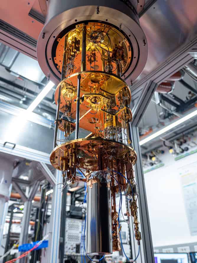
Cloud systems, however, can still hide too much. A polished interface can make a QPU look like a web service rather than a delicate machine. Students may not see the lasers that control ions or atoms, the cryostat that cools a superconducting chip, the microwave electronics that drive gates, or the human work behind calibration, where engineers tune the machine to keep it reliable. Cloud access teaches students to submit and analyse circuits. Access to hardware, control settings and error data helps them understand how the processor operates.

On-campus systems matter when students can inspect what sits behind the screen. In 2024 Rensselaer Polytechnic Institute in New York became the first university campus to host an IBM Quantum System One, initially powered by a 127-qubit Eagle processor. It is a striking example of a university putting a major machine within students’ reach.

Yet the educational value of any system depends less on qubit count than on what students can inspect, control and measure. A modest, accessible teaching platform – such as a photonic testbed that uses light to process information, a cryogenic set-up for testing devices at extremely low temperatures or a control-electronics lab that shows how signals drive qubits – can often teach more than a larger system that students cannot inspect.

Universities then should judge quantum-computing investments by learning outcomes, not headlines. Can students compare simulation and hardware? Can they test how a quantum computer changes over time by running the same circuit in the morning, afternoon and again the next day? Can they keep a notebook of circuits that worked in simulation but failed on hardware? Can they explain why one qubit pair works better than another? Can they connect algorithms to measurement, control, optics, microwaves, cryogenics and error reduction?

The experience has an emotional dimension too: a beautiful circuit on the whiteboard can become a difficult experiment on the chip. Students need to ask, “What algorithm did I write, and what physical experiment did the machine actually run?”

Students should feel the shock of an imperfect result, the frustration of a circuit that should have worked and the satisfaction of tracking down the physical cause. That experience turns quantum computing from a diagram into a craft.

A university quantum computer should be a teaching instrument that reveals the machine behind the calculation. Its purpose is to train people who can question claims, understand the hardware, and build the technology with sound judgement. The field needs graduates who understand the algorithm, the machine and the gap between them.

The post Universities should judge quantum-computing investments by what students learn appeared first on Physics World.

  •  

Using AI to plan for climate variability in renewable energy systems

Using solar and wind power for clean energy generation relies on the weather, which can be unpredictable. In addition to seasonal changes and daily variability, energy planners must also account for rare and extreme weather events. Traditional planning methods often fail to capture these events accurately, resulting in systems that are either overly expensive or insufficiently reliable.

In this work, the researchers aimed to develop a more effective way of planning energy systems that can cope with real climate variability. They built an artificial intelligence model trained on 30 years of wind and solar data from Pingtan in China. The model generated thousands of realistic weather scenarios, including both typical conditions and extreme events.

The researchers then used these scenarios to determine the most cost-effective and reliable combination of energy technologies. Their Integrated Energy System included solar panels, wind turbines, batteries, hydrogen production and storage, and a connection to the national electricity grid. The optimal system configuration was identified by testing its performance across all of the AI-generated scenarios.

The optimisation showed that the most effective renewable energy system combines several technologies working together. Wind and solar provide the main source of electricity, batteries manage short-term fluctuations in supply and demand, hydrogen storage provides backup during extended periods of low renewable generation, and the grid acts as an additional safety net.

The key finding is that batteries and hydrogen have complementary roles: batteries are best for balancing daily variations, while hydrogen is better suited to storing energy over weeks or months. Together, they help create a renewable energy system that is both reliable and cost-effective.

Do you want to learn more about this topic?

Energy policy and public opinion: patterns, trends and future directions by Parrish Bergquist, David M Konisky and John Kotcher (2020)

The post Using AI to plan for climate variability in renewable energy systems appeared first on Physics World.
  •  

Real-number quantum theory can be more wrong than you thought

Imaginary numbers first appeared in the 16th century as a mathematical invention, introduced to solve equations that real numbers could not. As the name implies, many treated them as kind of trick to get results, rather than an underlying truth about the nature of reality. Although highly controversial at the time, these numbers are now ubiquitous in many fields of physics and mathematics.

One such field is quantum mechanics. Researchers routinely use complex numbers, which include both imaginary and real parts. For many simple quantum systems, you could think this is a mathematical convenience rather than a physical necessity. Predictions made with complex numbers can often be reproduced using only real numbers, albeit in a larger mathematical space.

The key question is: are complex numbers merely just a convenience, a trick, or are they necessary to understand complicated quantum systems? And if they are necessary, to what extent?

A team of researchers from France, Poland and Spain have been working on this problem and they’ve now come up with an answer. Their work relies on the composition postulate – a standard starting point for formulations of quantum mechanics which describes how quantum systems are combined mathematically.

They set out by studying a star-shaped quantum network. In this network, a number of outer parties (N) each receive one part of a quantum system, while a central party (Eve) receives the other parts from independent sources.

Each outer party chooses between several simple two-outcome measurements, while the central party performs one measurement with many possible outcomes.

Their strategy was to build a specially designed, conditional Bell test. The most well-known Bell test compares classical physics with quantum mechanics, with experiments demonstrating the latter is a better description of reality.  However, Bell tests can compare the correlations predicted by many other different theories.

The two theories studied here were standard quantum theory using complex numbers and a different formulation of the theory only using real numbers. While it was already shown that complex numbers are necessary, just how much the predictions of complex and real quantum theories differ is still an open question.

They found that the ratio between the predictions of the two theories increased proportional to N-1. So as the network gets larger, real-number quantum theory becomes increasingly bad at reproducing the results of standard complex-number quantum theory.

The work therefore gives a clear answer to the original question. Namely, in sufficiently large quantum networks, complex numbers provide an advantage that can become arbitrarily large. If the composition postulate is respected, they are physically required.

Read the full article

Gap between quantum theory based on real and complex numbers is arbitrarily large – IOPscience

S. Sarkar et al 2026 Rep. Prog. Phys. 89 070503

The post Real-number quantum theory can be more wrong than you thought appeared first on Physics World.

  •  

Optical vortices provide a natural way to create topologies

Structured light is light with a designed spatial pattern. It can be shaped into standard topological structures, such as a twist in its phase or a changing polarisation across the beam. These patterns are useful because they can encode information, probe small distances and create topological field structures.

However, the issue is that is that these carefully engineered patterns often spread or degrade as the beam travels. This is a problem for real-world applications, such as precision metrology and super-resolution sensing.

In a new work, a team of researchers from Singapore and Spain went down a different route. They identified a spin structure which is both a topological texture and topological defect that is not laboriously engineered but appears automatically at the dark core of an optical vortex because Maxwell’s equations require it.

An optical vortex is a dark core in a light beam where the electric field vanishes. Because the field is zero there, the phase cannot be defined. The researchers found that the light around this core has a tiny, ordered spin pattern.

The called this a meronic spin defect. A meron is a texture that covers half of a sphere of possible spin directions, while a defect is a point where the direction becomes undefined. Here, both features occur together: the spin vanishes at the centre but forms a half-sphere-like pattern around it.

Crucially, these defects do not spread out during propagation. The beam might diffract as usual, but the normalised spin and polarisation patterns remain confined on subwavelength scales. They are also more stable against turbulence than standard engineered structures, because they arise intrinsically from Maxwell’s equations rather than from carefully balanced beam components.

Although still a fundamental result, the finding suggests that vortex cores could provide unusually stable and compact building blocks for future structured-light technologies.

Read the full article

Non-spreading meronic spin defects around optical vortices – IOPscience

N. Mata-Cervera et al 2026 Rep. Prog. Phys. 89 077901

The post Optical vortices provide a natural way to create topologies appeared first on Physics World.

  •  

Cling film helps stamp two-dimensional materials onto patterned surfaces

Since the discovery of graphene over two decades ago now, two-dimensional (2D) materials have revolutionized almost all areas of science and technology thanks to their unique properties compared with bulk materials. These include high electronic conductivity, high mechanical strength, transparency and flexibility, to name just a few. The problem since the beginning, however, has been to produce sheets of these materials large enough for real-world applications and, importantly, to be able to transfer them onto other substrates without cracking the sheets. A team of researchers in Amsterdam, the Netherlands, has now succeeded in doing just this, with the help of an unexpected material – kitchen cling film. Their work could help in the continuing development of next-generation electronic and optoelectronic devices.

“The method we developed allows us to, for the first time, pick up, transfer and place large (roughly 1-mm-sized) 2D layers on almost arbitrarily patterned surfaces,” explains Jorik van de Groep of the 2D Nanophotonics group at the UvA-Institute of Physics, who led this research study. “Being able to do this is crucial since it enables the integration of 2D materials with structures like larger electronic devices and photonic coatings. Most importantly, the transfer is no longer probabilistic (as were most other methods) but has a near-unity yield.”

In the early days of 2D materials, researchers obtained micron-sized mono- or multi-layers of these structures by mechanically shaving off, or exfoliating, flakes from the bulk material using sticky tape. This was first famously done for graphene, a sheet of carbon just one atom thick. More recently, a technique known as gold-assisted exfoliation has allowed them to produce high-quality centimetre-sized layers of technologically important materials like transition-metal dichalcogenides (TMDCs) and transfer these onto flat glass surfaces.

For the field of nanophotonics in particular, explains van de Groep, we need to be able to transfer large-area 2D materials onto both flat and patterned substrates – such as those with electrical contacts and optical coatings on them, for example – if we are to fabricate functional devices. The problem is that existing transfer techniques are limited in this respect.

Kitchen cling film to the rescue

The Amsterdam team – which also includes researchers from UvA’s Van ‘t Hoff Institute for Molecular Sciences, ARCNL and AMOLF – has now developed a simple method that allows them to reliably transfer both large-area monolayers of TMDCs and hexagonal boron nitride/monolayer heterostructures onto patterned or non-patterned substrates, ranging from flat surfaces to high-aspect ratio and low adhesion patterned interfaces. In their process, which is detailed in ACS Nano, they used low-density polyethylene (LDPE), or kitchen cling film, an inexpensive and widely available polymer that has a low melting temperature.

In their work, the researchers transferred a gold-assisted-exfoliated large-area monolayer of the TMDC tungsten disulphide (WS2) from a silica (SiO2) substrate to another target SiO2 substrate. They began by fabricating a stamp made of a heat-resistant half-sphere covered by LDPE cling film. They then mounted the stamp on an xyz-micron precision stage and moved it slowly towards the WS2 monolayer, which was heated to 70 °C, at a speed of 0.5 µm/s until it contacted with the LPDE.

“We used force sensors in the stage to measure the forces involved during the stamping procedure, both in the plane of the 2D material (Fx and Fy) and perpendicular to it (Fz),” explains van de Groep. “This not only offers better control and repeatability of the transfer, it also provides crucial information on the contact and friction dynamics throughout the process.”

During initial contact with the substrate, the normal force (Fz) increases to 120 mN, at which point the researchers stop moving the stamp. Once it has contacted the monolayer, they heat the system to 140 °C. This induces a phase transition at which the LDPE melts, so allowing it to strongly adhere to the monolayer. They then cool the ensemble back down to 70 °C to solidify the LDPE. Finally, they pull off the monolayer from the LPDE with the stage moving at 0.5 µm/s and clean it to remove any polymer residue.

Material retains its good photoluminescence properties

To assess how the transfer process affects the monolayer, the researchers imaged it before and after the procedure. Before transfer, cracks covered 8% of the material. This figure increased to 14% after, with the cracks mainly generated at the edge of the stamp contact area. “As such, the procedure only modestly increases the cracked area fraction and largely preserves the monolayer topography,” says van de Groep. “More importantly, the material retains its good photoluminescence properties.”

The new work could help 2D materials scientists working in a variety of different fields to build larger and more complex devices. “Already, we are using it to develop atomically thin optical elements, optical modulators, single-photon emitters and other optoelectronic devices,” van de Groep tells Physics World. “Also, and more fundamentally, the method we have developed could allow for the fabrication of complex heterostructures of interest for quantum materials.”

The Amsterdam team is now busy optimizing its method further by, for example, building a humidity-controlled environmental enclosure around the stamping setup. “2D materials and the (van-der-Waals) adhesion between them strongly depends on the surface chemistry and, as such, on the relative humidity during the stamping procedure,” explains van de Groep. “We’re also working on additional methods to characterize the thickness of the materials in situ, that is, during the stamping process.”

The post Cling film helps stamp two-dimensional materials onto patterned surfaces appeared first on Physics World.

  •  

Missing decay at BESIII points to long-sought glueball

Physicists at China’s BESIII experiment in Beijing have found the strongest evidence yet for the existence of glueballs – subatomic particles made of gluons alone. The glueball-like particle is called X(2370) and it was first spotted at BESIII 15 years ago.

Gluons carry the strong nuclear force that binds quarks into protons and neutrons. Gluons also pull on each other as hard as they pull on quarks, which means they ought to be able to clump into particles called glueballs.

“So far, all ordinary matter that we know of is composed of quarks and leptons,” says Colin Morningstar of Carnegie Mellon University, whose 1990s supercomputer simulations helped predict what glueballs should look like. “A glueball is a totally new form of matter made up entirely of gluons – no quarks, no leptons,” explains US-based Morningstar, who is not a member of the BESIII team.

For four decades, detecting glueballs have been an important goal of BESIII and its predecessor – according to Shan Jin of China’s Nanjing University. BESIII is on the BEPCII accelerator, where electrons collide with positrons to create large numbers of J/ψ particles. A J/ψ can sometimes decay by shedding a flash of light and dumping the rest of its energy into gluons. The gluons could then bunch together to create a glueball.

Lightest glueball

In 2011, Yanping Huang was Jin’s PhD student and observed the production of the short-lived X(2370) particle at BESIII. “The most important next step was to determine its spin-parity quantum numbers, and it turned out to be one of the most difficult steps for us due to large background processes,” says Huang, now at China’s Institute of High Energy Physics in Beijing. Those numbers describe how a particle behaves when turned around and seen in a mirror – a kind of fingerprint. Only in 2024, with an exceptionally clean chain of decays and all 10 billion J/ψ particles, could the team read it, and it matched the prediction for the lightest glueball.

Now, Huang, Jin and the rest of the BESIII team have gone further and searched in vain for a specific X(2370) decay channel. They argue its absence suggests that X(2370) contains no quarks and the lightest glueball is its dominant constituent.

Quarks come in several types, or flavours, and a glueball contains none, so it cannot favour one flavour over another. That even-handedness forbids the X(2370) from breaking up into a particular pair of kaons, which are lightweight particles carrying a strange quark. BESIII looked for that break-up and found that the decay occurs at a rate that is at most 8% of the rate of a much more common X(2370) decay channel.

Huang explains that an ordinary quark-based particle should undergo the kaon-pair decay far more often. “The lightest glueball is essential for a natural and complete explanation of all these properties, while all other interpretations can hardly explain them simultaneously”.

Like a duck

Francesco Giacosa at Jan Kochanowski University in Poland is enthusiastic about the BESIII research, which he was not involved with. “We have an object, X(2370), that walks like a duck, quacks like a duck and, in addition, does not do something that the duck we are searching for should not do.”

Jin says that the BESIII result has important implications. “This is the direct proof of self-coupling among gluons predicted by QCD about 50 years ago,” where QCD is quantum chromodynamics, the theory of the strong force. It also illuminates the origin of mass, “since the gluon mass is zero and the glueball mass is totally from the strong interaction”. Glueballs, he says, are “a unique kind of matter made of pure force”.

Morningstar observes, “The results are the strongest evidence yet that particles dominated by a glueball component can exist in nature. This work is certainly an experimental triumph.”

Not everyone is ready to call the 50-year search over. “In my opinion, an independent experimental confirmation would be extremely important,” says Giacosa. A glueball can also blend with ordinary quark particles, he notes, so “even if X(2370) is predominantly a glueball, we do not know precisely how large its non-glueball component is”.

Upgrade needed

Gentler collisions elsewhere could shed further light on this, says Jin, “but it seems difficult for them to collect 10 billion J/ψ events to perform systematic studies as BESIII in a short time, unless we upgrade BEPCII itself again”.

That upgrade is on the collaboration’s wish list. Huang plans further measurements of the particle’s properties, which “will also certainly help us to identify more glueballs”. Reaching them may take ten times more data.

Morningstar also looks forward to further discoveries, “Our theoretical computations have suggested other glueballs that might exist, so with this successful study, I believe the search for other glueballs will intensify”.

Giacosa thinks the prize is worth it. “Glueballs are, in my view, among the most fascinating composite objects predicted within the Standard Model,” he says, meaning physicists’ theory of the fundamental particles and forces. “Establishing one experimentally would be much more than adding one more particle to the list – it would confirm one of the most remarkable predictions of the theory of the strong interaction.”

The results were presented in August at the International Conference on High Energy Physics and are described in a preprint on arXiv.

The post Missing decay at BESIII points to long-sought glueball appeared first on Physics World.

  •  

Researchers shrink double-slit experiment to atomic scale

Shrinking Young’s double-slit experiment
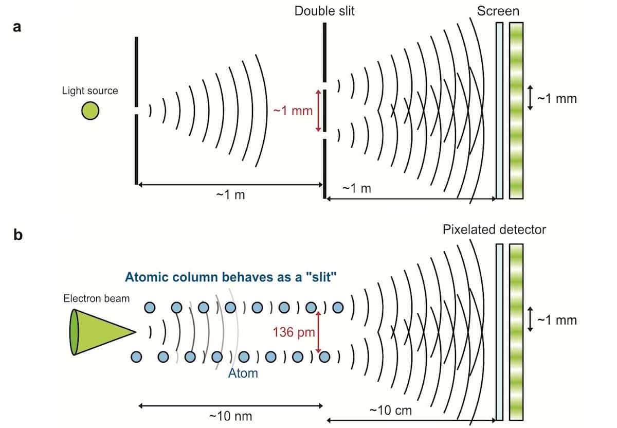
Shrinking Young’s experiment (a) The classical double-slit experiment using light (slit spacing ~1 mm, propagation distance ~1 m). (b) Schematic of atomic-scale interference in which a pair of neighbouring silicon atomic columns act as a “double slit” for a focused electron probe (spacing 136 pm; crystal thickness ~10 nm; distance to detector ~10 cm). (Courtesy: Koudai Tabata/University of Tokyo)

For the first time, physicists in Japan have carried out an atomic-scale version of the double-slit experiment. Using an ultraprecise electron beam channelled along two adjacent columns of atoms in a crystal of silicon, Naoya Shibata and colleagues at the University of Tokyo observed clear interference fringes in electrons scattered by the atoms: fringes that persisted even at high temperature, thanks to correlations in the atoms’ thermal vibrations.

The double-slit experiment is perhaps the most iconic demonstration in quantum mechanics: showing how a single particle’s wavefunction interferes with itself as it passes through two slits at once, with a tangible impact on where the particle is ultimately observed.

In practical research, this effect is now routinely harnessed in electron, neutron and atom interferometers. By observing the interference fringes that it creates, researchers can extract valuable information about both the quantum matter wave and whatever object is doing the diffracting.

Recently, physicists have attempted to push double-slit interferometry all the way down to the atomic scale, replacing conventional slits with crystal lattices. When a moving electron encounters an atom in a crystal, it scatters across a range of angles – producing an outgoing spherical wave that’s mathematically identical to the diffraction pattern from a classical slit.

Since atoms in a crystal sit at such well-defined separations, any neighbouring pair of them could, in principle, act as a double-slit interferometer. In reality, however, the many repeated unit cells in a crystal mean the resulting interference fringes are washed out, making it difficult to isolate the signal from a single atomic pair.

To address this challenge, Shibata’s team used the ultraprecise probe of a 4D scanning transmission electron microscope: an instrument designed to capture electron diffraction patterns with a pixellated detector. Fired into a pure silicon crystal at just the right orientation, the microscope’s precision let the researchers target two adjacent columns of aligned silicon atoms, separated by just 136 pm. As a result, the electron wave overlapped both columns, and no others.

“Our key idea was to use these two atomic columns as the two slits,” describes team member Takehito Seki. “By channelling the probe along both columns at once, we turned them into two coherent scattering sources – effectively making the crystal itself into an atomic-scale double-slit interferometer.”

At this scale, Shibata and Seki’s team created electron interference fringes some seven orders of magnitude smaller than in Thomas Young’s original double-slit experiment with light, first carried out in 1801.

Just as in a larger-scale experiment, these patterns encoded information about the crystal and the electron beam. But at this scale, the researchers could also detect the signature of individual phonon modes in the columns. Rather than destroying coherence as uncorrelated atomic motion would in a classical picture, these correlated vibrations between the two atomic columns kept them moving in sync, preserving the interference.

“In a which-path picture, relative motion of the two atomic columns makes the two electron pathways more distinguishable and reduces the interference, whereas correlated in-phase motion preserves coherence,” Shibata explains. As a result, distinct interference fringes remained visible across temperatures ranging from 300 to 900 K.

The team’s results already point to how an atomic-scale double-slit experiment could offer new ways to measure phonon correlations directly between single pairs of atoms. But as Shibata explains, the possible applications could stretch much further.

“It also opens a route to probing local lattice dynamics at the scale of individual atomic bonds, including at interfaces and defects, where local lattice dynamics can strongly influence thermal transport,” he says. “In the long run, such atomic-scale insight could help inform better thermal management strategies for future chip technologies.”

The study is published in Nature.

The post Researchers shrink double-slit experiment to atomic scale appeared first on Physics World.

  •  

Noise that entangles may accelerate the dawn of quantum technologies

Qubits are delicate and often misbehave. A qubit’s advantage over an ordinary bit is that in addition to “0” or “1”, it can hold values of 0 and 1 at once, in a specific combination; that combination is what quantum algorithms actually run on. But any stray interaction with the surrounding world (a vibration, a stray field, a single errant photon) leaks out a bit of information about which state the qubit is in – and that’s enough to collapse the combination back into an ordinary, classical either/or state. Coupling to the environment leads to high decoherence, meaning high error rates, and is normally how we lose good quality qubits. As such, most of the engineering effort in quantum computing goes into avoiding this coupling.

Yet recently, a team at the Institute of Science and Technology Austria (ISTA), working with collaborators in Munich and Madrid, has defied this norm.

Writing in Physical Review X, Alejandro Andrés-Juanes, Johannes Fink and colleagues show that two superconducting transmon qubits, separated by a metre of coaxial cable, can settle into an entangled state by being exposed to the same quantum-correlated microwave field. Avoiding synchronized pulses, heralding, post-selection and feedback (techniques usually used to actively generate and verify entanglement, rather than to fix decoherence), the entanglement can be generated and maintained for as long as the field is on. In other words, the researchers have managed to exploit noise to generate entanglement, rather than losing their qubits to it.

This idea of entangling by using fields belongs to a family of techniques known as dissipation engineering. “The common understanding is that the environment is bad, and it will decohere your qubits,” Andrés-Juanes tells Physics World. “The main idea [here] is that one can engineer a specific interaction with the environment that is not detrimental but – like in this case – prepares your qubits in an interesting state without you having to actively apply any action on the system.”

This proposal dates back more than 20 years, to work performed by Barbara Kraus and Ignacio Cirac, but this is its first experimental realization.

The correlated environment comes from a superconducting device (a Josephson parametric converter) that splits each pump photon into a pair of photons at gigahertz frequencies. The two photons of this pair are entangled with one another and each is sent down its own coaxial cable to one of the qubits, half a metre away in either direction.

Quantum research at ISTA
Quantum research The lab at the Institute of Science and Technology Austria. (Courtesy: © ISTA)

Because the noise reaching the two qubits is correlated, relaxing into it does not scramble them (specifically, it does not wash out the fixed phase relationship between them, as independent noise on each qubit would). They settle instead into a superposition, for which absorbing a photon from the field and emitting one into it interfere destructively: “the destructive interference between a photon emission event in the first waveguide and a photon absorption process at the location of the second qubit,” as the authors explain.

Once there, the qubits stop evolving and the field passes through unchanged: the entangled state is dark, invisible to the very field that created it. What the experiment does, in effect, is convert the continuous-variable (CV) entanglement carried by the two microwave beams into ordinary entanglement between two conventional transmon qubits – “we obtain qubit entanglement from CV entanglement,” Andrés-Juanes confirms – with roughly a tenth of it inherited.

Most entanglement-distribution schemes deliver entanglement as events: a pulse sequence runs, a detector clicks, a pair is announced, and the state then decays until the sequence runs again. The author’s autonomous version could enable the elimination of this machinery.

“It removes a lot of overhead on the pulse sequences you need to run to get the entanglement,” says Andrés-Juanes, an advantage that’s expected to matter most at scale, since one correlated photon source can drive many pairs at once. “Another differential feature of this protocol is that the entanglement is ‘always on’ for when you need to use it. In active protocols, you would have to reinitialize the entangled state because it would decohere after a while.”

The practical limit of this setup is temperature: “We use microwave frequencies, which are only quantum at very low temperatures,” Andrés-Juanes explains. “The real limit in the separation is how big your dilution refrigerator is”, with the longest such link so far being 30 m, at ETH Zurich. He positions the work as an intermediate-distance technology rather than a long-distance one. At optical frequencies, the constraint would lift, though achieving the same strong qubit–waveguide coupling in an atomic system would be its own problem.

For now, the numbers are modest: two qubits, entangled with a concurrence of just 0.10 (on a scale where 1 is a perfect pair), inheriting only about a tenth of the entanglement carried by the microwave beams. The group is working on a module with more than one qubit per node.

But critically, the idea is no longer theoretical. The team has now realised an entangled link that is always “there”, bringing us one step closer to distributed quantum computing (linking separate processors into one machine via entanglement), networked sensing (detectors sharing entanglement to jointly see what none could alone) and quantum repeaters (relay stations for long-distance quantum links, needed because a quantum state can’t be copied and amplified like a classical signal).

The post Noise that entangles may accelerate the dawn of quantum technologies appeared first on Physics World.

  •  

Magnetism likely played a key role in early solar system formation

The oldest known solids in the solar system contain evidence that the protoplanetary disc that went on to form the planets around our Sun experienced a magnetic field stronger than the field on Earth today, new research suggests. Study of inclusions in a primordial meteorite called a carbonaceous chondrite indicates that magnetism needs to be considered in simulations of planet formation, and may even be the dominant factor.

When planetary systems condense, they initially form high-temperature molecular nebulae. These later cool and accrete into planets surrounding central stars – which, at some point, begin to undergo nuclear fusion. Even before this happens, however, the gas is highly ionized. “A good portion of the ionization is coming from the molecular cloud itself,” explains planetary scientist Cauê Borlina of Purdue University. “It’s a combination of radiation from space and high temperature.”

In any ionized system there is the potential for magnetic fields, but simulations of disc formation often take no account of them, partly as they remain poorly constrained: “It’s a lot easier to just crank up the gravity and use that as a way to match the accretion rate,” says Borlina.

The new study from Borlina and colleagues in the US, China and the UK provides an unprecedented peek at fields in the terrestrial planet-forming region in the first 500,000 years of the Solar System’s existence – before the Earth had formed – using calcium-aluminium-rich inclusions. These are the oldest known solar system solids, comprising minerals with extremely high melting points that are inclined to condense early. “It is very unlikely to get them at later stages,” says Borlina. Previous researchers have confirmed their ages using isotopic dating.

Millions of years after these inclusions formed, they agglomerated with other protoplanetary material into planetesimals, some of which went on to form planets. Planetary scientists think the remaining material accreted to form the chondrites – which astronomers distinguish into several different types depending on their chemical composition. When they fall to Earth as chondrite meteorites, therefore, they provide a valuable glimpse into the solar system’s raw material.

Carbonaceous chondrites hold particular interest as they are thought to have the most primitive chemical compositions of all meteorites. The researchers studied calcium-aluminium inclusions in the 667 g Dominion Range 08006 carbonaceous chondrite discovered in Antarctica in 2008. Such inclusions had, until around 2010, been thought to contain no magnetic minerals. Borlina and colleagues, however, found that some – although not all – of the inclusions contained nanometre-scale amounts of ferromagnetic iron-nickel.

The researchers measured the thermoremanent magnetization of these iron-nickel grains (the field strength they experienced at the time when they cooled down through their “Curie temperature”, thereby fixing their own magnetism). In theory, this could be achieved by heating the sample above the Curie temperature, which for iron-nickel is about 1050 K, and measuring the field required to demagnetize it. Unfortunately, says Borlina, heating meteorites up in the laboratory tends to oxidize the materials extremely quickly, making reliably calibrated experiments very difficult.

Instead, the researchers used an established method called anhysteric remanent magnetization, concluding that the inclusions were exposed to fields of 150–600 µT when they cooled through the Curie temperature (the field on Earth today is around 30–60 µT). “This is good evidence that…you can’t just ignore magnetic fields,” says Borlina. “They need to be present in your simulations.”

The researchers are now studying other carbonaceous chondrites and other types of chondrite meteorites – some of which are thought to have formed in different regions of the protoplanetary disc – hoping to gain a fuller picture of how magnetism shapes disc evolution. “The idea was to put it out there that there’s this new inclusion that might hold magnetic carriers, and there’s a lot of work to be done,” says Borlina.

Meenakshi Wadhwa of University of California, San Diego – who formerly directed the Center for Meteorite Studies at Arizona State University – describes the work as “genuinely significant”. First, she says, it provides the first definitive paleomagnetic signal from a carbonaceous chondrite. Second, the estimated field is multiple times previous estimates.

“Yes, the sample size is small (five inclusions from a single chondrite), but I think the authors make a reasonably solid argument for their conclusions,” she says. The next step, she concludes, “is to measure inclusions from other chondrite groups to see if the signal is reproducible, and to test whether it’s a real nebular record versus something very localized, specific to DOM 08006 or the carbonaceous chondrite reservoir. Beyond that…pinning down when and where inclusions acquired their magnetization will also be important.”

The research is published in Proceedings of the National Academy of Sciences.

The post Magnetism likely played a key role in early solar system formation appeared first on Physics World.

  •  

Astronomers discover unusual 10-sided atmospheric wave on Saturn

While Earth’s atmosphere is constantly changing, many spectacular storms and atmospheric waves on Saturn remain stable for decades or even centuries.

Images from NASA’s Voyager craft as it flew-by the planet in the early 1980s revealed a large and long-lived hexagonal atmospheric wave around Saturn’s north pole.

Yet despite decades of observations from other craft such as the Cassini mission, no similar wave has been reported in the southern hemisphere or elsewhere.

Now, Agustín Sánchez-Lavega from the University of the Basque Country in Bilbao and colleagues have spotted a growing decagon-shaped wave around the planet’s south pole.

The researchers discover the phenomenon thanks to images from NASA’s Hubble Space Telescope as well as ground-based telescopes as the planet’s south pole came back into view from Earth due to Saturn’s axial tilt.

It seems that the 10-sided wave developed between 2023 and 2025 and may still be evolving, in contrast to the 40-plus years of steadiness shown by the hexagon.

The longitudes of the decagon’s vertices oscillate over a period of 32 days, and its movements suggest it may be trapped by the curvature of an atmospheric jet.

The researchers suggest the wave could have been created by a spatially periodic disturbance in the jet peak or driven by an “anticyclonic vortex” to its north.

However, further study is required to better understand how it formed and how it compares to the hexagon structure in the north.

“The most intriguing part to me is that this seems to have just formed recently,” notes study co-author Amy Simon from NASA’s Goddard Space Flight Center in Maryland. “The question is, why did it suddenly form now when we haven’t seen one before?”

The post Astronomers discover unusual 10-sided atmospheric wave on Saturn appeared first on Physics World.

  •  

‘Lid’ of asteroid dust smothered and burned the dinosaurs, say scientists

As wildfires and extreme heat events rage across the world, “apocalyptic” has become an increasingly common descriptor. These climate disasters are not unprecedented, however. New research suggests they may have been the main mechanisms behind the mass extinction event that killed the dinosaurs – and much other life on Earth – 66 million years ago.

Our modern understanding of this extinction dates back to 1980, when the father-and-son, physicist-and-geologist team of Luis and Walter Alvarez presented evidence that it was triggered by an asteroid strike. Subsequent work identified the Chicxulub crater in Mexico’s Yucatán Peninsula as the likely impact site, but debate has persisted – including over how a single asteroid could cause worldwide destruction.

In the latest work, Brandon and Alexandria Johnson, a husband-and-wife duo at Purdue University in the US, fit another piece into this puzzle. By combining Brandon’s research on impact cratering with Alexandria’s expertise on the behaviour of atmospheric particulates, they found that the asteroid impact sent up a near-impermeable layer of dust that smothered the entire planet. Their research, published in Journal of Geophysical Research: Biogeosciences, breathes new life into a theory that had fallen out of favour: that extreme heat and wildfires were the main killers on the day the asteroid hit. 

The key to ignition

At some level, this dust layer likely produced a cooling effect, much as large volcanic eruptions do today. Indeed, a previous study showed that condensed droplets of rock known as spherules would have blocked the Sun’s radiation from entering the atmosphere.

At the Earth’s surface, however, the Johnsons think the dinosaurs had the opposite problem. The impact also sent a massive plume containing over 1000 km3 of vaporized material high into the atmosphere. When this material rained down as spherules, the dust cloud’s potential cooling effect was reversed.

“[The spherules] are essentially adding energy back to the atmosphere by travelling through it to the surface. That energy has to go somewhere,” Alexandria Johnson explains. “What we found is that this dust layer over the planet is essentially acting like a lid, and it’s keeping almost all the radiation that should try to find its way back out to space and reradiating it back down to the surface. So it’s enough to not only kill the dinosaurs but actually start widespread wildfires.”

Both researchers were surprised at just how opaque this dust layer was. By their reckoning, it trapped almost all radiation within the atmosphere, allowing a staggeringly tiny upwards transmittance of just 10-286. 

“I asked [Brandon] to redo my calculation, I was like ‘make sure these numbers are right’, because this is absolutely nothing,” says Alexandria. “I expected more than what we got to be reradiated out, but the fact that it doesn’t just enhances the whole idea of the heat pulse killing things off in a very quick manner.” 

Based on the Johnsons’ estimated heat fluxes, any creatures that couldn’t shelter or burrow – dinosaurs included – would have suffered temperature-induced deaths within an hour or two of the impact. The radiation was also more than enough to ignite lichens, grasses and pine needles, destroying vast amounts of plant life through wildfires. 

Never-ending night

Anything that survived the heat then had to face the darkness. “You would have had darkness lasting for a long time which then can cause collapse of the food chain in the oceans and cause oceanic extinctions,” says Brandon Johnson. The dust particles were about as small as those in wildfire smoke, and they may have blocked out the Sun for as long as decades before settling into what we now see as the K-Pg boundary: a rock layer a few millimetres thick that contains high levels of iridium, identified by the Alvarezes as coming from an asteroid.

Although some previous works suggested that the impact couldn’t have ejected enough material to trigger such large-scale effects, Brandon says his analysis of rock vaporization thresholds indicates that the plume’s mass was big enough to facilitate the transport of material across the planet’s atmosphere. Without this transport, he adds, the wreckage would have been more localized to the Chicxulub impact site. 

Given the interdisciplinary nature of the field, Brandon thinks there are many ways this line of research could continue. Possibilities include investigating the geological record in more detail and combustion experiments to better understand the wildfires’ impacts. He himself is hoping to carry out 3D impact simulations which can more accurately incorporate the vaporization of rock. “Essentially, [we want] to see what happens to that vapour and see if it is going to expand and be deposited globally as we expect,” he says.

The post ‘Lid’ of asteroid dust smothered and burned the dinosaurs, say scientists appeared first on Physics World.

  •  

Finding careers in STEM and the weirdness of AI

This episode of the Physics World Weekly podcast features two conversations. The first is with career consultant Alaina G Levine who gives advice on how to build a “unicorn career” in science, technology, engineering, and mathematics. Our second guest is the optics and artificial-intelligence researcher Janelle Shane who writes extensively about the absurd, and often hilarious, side of AI.

Levine’s latest book is called Create Your Unicorn Career and Shane writes about artificial intelligence on her blog  AI Weirdness.

This podcast is supported by American Elements, the world’s leading manufacturer of engineered and advanced materials. The company’s ability to scale laboratory breakthroughs to industrial production has contributed to many of the most significant technological advancements since 1990 – including LED lighting, smartphones, and electric vehicles.


The post Finding careers in STEM and the weirdness of AI appeared first on Physics World.

  •  

Antineutrino detector could monitor spent nuclear fuel for clandestine activity

Scientists have measured antineutrino emissions from spent nuclear fuel for the first time, demonstrating that monitoring efforts need not stop when the reactors do. This is important because although independent nuclear safeguarding agencies have long used antineutrino emissions to glean information on reactor operations, previous detection schemes only worked when the reactors were running. Now, however, members of the Double Chooz collaboration have shown that it is possible to detect residual antineutrino emissions during a complete reactor shutdown – including from spent fuel stored in cooling pools.

Like neutrinos, antineutrinos are tiny, nearly massless fundamental particles that come in three flavours: electron, muon and tau. The largest human-made sources of electron antineutrinos are the reactor cores of nuclear power plants, which produce them via beta decay of neutron-rich fragments that are primarily generated during the fission of heavy elements such as uranium and plutonium.

Because antineutrinos interact so rarely with other particles, their emissions cannot be shielded and their signatures cannot be altered. They can also be detected some distance from the power plant itself. All these features make them valuable for nonintrusive nuclear reactor monitoring. Indeed, the idea of using antineutrinos to provide real-time information about the fissile content of a reactor core – and thereby detect illicit production of material that could be used in nuclear weapons manufacturing – dates back to the 1970s.

When a reactor is shut down, long-lived fission products (found in burnt fuel assemblies that remain in the reactor core, as well as assemblies that were previously removed and stored in nearby cooling pools) continue to decay, producing a residual neutrino flux. However, this residual signal is only around 1% as strong as the signal from an operating reactor. It also lies in a region of the energy spectrum that is strongly affected by background activities.

Measuring the residual neutrino flux and its energy spectrum

In the new work, which is detailed in Physical Review Letters, a team led by Thierry Lasserre and Anthony Onillon from the Max-Planck-Institut für Kernphysik (MPIK) in Heidelberg, Germany, succeeded in measuring the residual neutrino flux and its energy spectrum despite these difficulties. They obtained their data from the Double Chooz neutrino detection experiment, which is located near the two 4.25 GWth cores of the Chooz B nuclear power plant in the French Ardennes. This experiment uses a pair of detectors – labelled “near” and “far” and located around 400 m and 1.05 km from the cores – to study a fundamental parameter called the 𝜃13 neutrino mixing angle that describes how neutrinos transform between different types as they travel.

The Chooz plant uses a pair of pressurized water reactors, each of which contains 205 fuel assemblies consisting of roughly 600 kg of enriched uranium dioxide (mainly 238U with a few percent of 235U). During operation, these reactors also produce additional fissile isotopes, 239Pu and 241Pu, through neutron capture and subsequent decay processes involving 238U. In a typical cycle, they operate at full power for over a year and are then shut down for six to eight weeks for refuelling. During this time, some of the spent fuel assemblies are removed and transferred to storage pools in a nearby building.

The Double Chooz neutrino detector consists of more than 30 m3 of liquid scintillator, which is a material that emits short, double flashes of light when an antineutrino hits it. The outer part of the detector is shielded from the background radiation of the surrounding mountain rocks by 15 cm of demagnetized steel for the far detector and 1 m of water for the near detector. The inner part of the detector is shielded by a thick layer of mineral oil. Finally, an outer “muon veto” consisting of segmented scintillator modules positioned above the detector eliminates contributions from cosmic muons that can mask the signal from the antineutrinos.

Over 100 events observed

The researchers collected their data in 2017 when both of Chooz’s reactors were simultaneously shut down for 24.4 days for refuelling and maintenance. This unusual double shutdown was long enough for the team to obtain the statistics and low background signals needed to extract, for the first time, a quantitative residual reactor antineutrino spectrum.

After accounting for muon veto-induced dead time, the researchers clocked up 17.2 days of measurements for the near detector and 22.2 days for the far detector. While they analysed data from both, they mainly focused on the near detector because it is closer to the reactor cores and spent fuel pools and is therefore more sensitive to the residual antineutrino flux.

In the 1–3 MeV range, where the residual neutrino signal is strongest, the researchers observed 106 ±18 events, which represents a 5.9 σ excess over the background. This value, they say, is in very good agreement with the 88 ±7 events predicted by detailed simulations of the remaining nuclear fuel inventory and the decay of long-lived fission products.

According to the researchers, this result had a long gestation period: “In 2003, the IAEA safeguards met with the neutrino community and raised a question: could antineutrinos also provide information on spent nuclear fuel?

“The main difficulty has been detecting the faint residual antineutrino signal. This meant obtaining data during periods when both Chooz reactors were simultaneously off, very low and well-controlled detector backgrounds, and a detailed simulation of the irradiation and cooling history of relevant fuel assemblies.”

The researchers hope that their result will become a robust benchmark for agencies and experimenters designing detectors for specific spent-fuel monitoring applications. “Such monitoring is feasible and could provide an independent, non-intrusive complement to reactor-status and spent fuel inventory,” they tell Physics World, though they add that “it will not necessarily be easy, compact or inexpensive to implement.”

The post Antineutrino detector could monitor spent nuclear fuel for clandestine activity appeared first on Physics World.

  •  

Plasmonic metamaterial makes a photonic time crystal

Researchers in France and Germany have created the first all-optical photonic time crystal. The nanostructure could be used to make ultrafast optical computers and amplifiers, frequency converters and perhaps even new types of lasers that work in the terahertz range.

Photonic crystals are nanostructured materials with a refractive index that varies on a length scale comparable to the wavelength of light, producing a phenomenon known as a photonic bandgap. This gap affects how photons propagate through the material in a way that resembles how a periodic potential in semiconductors affects the flow of electrons by defining allowed and forbidden energy bands. In the case of photonic crystals, light in certain wavelength ranges can pass through the material, but other wavelengths cannot.

Photonic time crystals (PhTCs) are similar to this, except their properties vary periodically in time, not space. Among other adjustments, this means that instead of photonic bandgaps, they host momentum bandgaps. These gaps are special in that light waves whose momenta fall within them grow exponentially in time.

Optical modulation at THz frequencies

PhTCs show much promise for applications like new types of tuneable lasers and ultrafast frequency converters, but controlling their photonic properties has proven very difficult. This is because these properties need to be modulated very strongly and on ultrashort timescales – on the order of the temporal period of the light itself.

Producing such extremely fast modulations is a key goal for scientists working in a branch of highly nonlinear optics known as time-domain photonics. Previously, their efforts have paid off in the microwave frequency range using PhTCs containing electrical circuits, but all-optical systems have proven elusive.

A team of physicists led by Yannis Laplace of the Ecole Polytechnique in France has now made a PhTC with properties that can be optically modulated at terahertz (THz, 1012 Hz) frequencies. The new PhTC is made from a type of photonic crystal known as a plasmonic metamaterial: an artificially engineered nanostructure consisting of micron-sized cavities made of gold atop an insulating layer and a semiconductor material based on indium and antimony. The cavities trap photons between the gold and semiconductor layers, and surface plasmons – collective, coherent oscillations of conduction electrons that interact very strongly with light – then keep them on the surface of the semiconductor.

Working with scientists from the Collège de France and the Helmholtz-Zentrum Dresden-Rossendorf (HZDR) in Germany, the researchers applied pulses of THz light from the TELBE light source at the HZDR’s ELBE accelerator to their structure. They found that they could use this intense multi-cycle THz light field to modulate the material’s optical properties over timescales of just picoseconds.

Towards new types of lasers in the THz range

“This study builds on previous work in my group related to the development and study of tuneable plasmonic metamaterials in the THz range as a means to create functional devices to control light-matter interactions in this range,” Laplace says. “One of the central questions in our work was to determine if the temporal modulation of the metamaterial would be strong and fast enough.

“By developing a theoretical model in collaboration with our colleague Marco Schiró and his team at the Collège de France that reproduced the experimental observations remarkably well, we showed that the system presented the characteristic spectroscopic signatures expected for a PhTC and provided an explanation for the behaviour of the photons therein.”

The researchers, who detail their work in Nature, also found that the ultrafast temporal modulation reduced the dissipation of photons within the metamaterial by half and they are now looking to reduce these optical losses even further.

“The THz frequency range lies at the junction between electronic and photonic technologies and is historically less developed than these two,” Laplace explains. “With the THz PhTCs that are now achievable, we hope we can soon develop devices like THz amplifiers, frequency converters and maybe new types of THz lasers in this range, hence contributing to the closing of the so-called ‘THz gap,’” he tells Physics World.

The post Plasmonic metamaterial makes a photonic time crystal appeared first on Physics World.

  •  

Two-dimensional material shows promise for long-term memory, thanks to slow electrons

Two-dimensional (2D) materials have attracted a lot of attention in recent years for their excellent electronic, thermal and mechanical properties, as well as their interesting quantum effects. While graphene has gathered the most commercial attention, there are hundreds of 2D materials, all of which have different combinations of properties for different applications. A research team headed up at the University of Chicago has discovered some unusual behaviour in the 2D material Fe5GeTe2.

Some 2D materials exhibit superconductivity properties and charge orders (in which the electrons are confined in a specific arrangement rather than being able to move freely). Charge orders arise from the reshaping of ground states in the electronic bands of a 2D materials to create flat electronic bands. And these flat bands cause the electrons to move very slowly in the lattice, at speeds much slower than expected.

Extremely flat electronic bands can often become incoherent, due to an ultrastrong electronic interaction strength between charge carriers. In research published in Science Advances, Shuolong Yang and colleagues found that Fe5GeTe2 exhibits a charge-ordered state where electrons move both collectively and very slowly, while remaining quantumly coherent.

“I was originally motivated by the fact that Fe5GeTe2 was discovered to host multiple structural phases with nearly the same stoichiometry. Each structural phase is associated with its unique electronic and magnetic phase,” says Yang. “These different structural phases have almost degenerate energies, which means that they can all be stabilized at room temperature.”

According to Yang, this discovery prompted two key research questions: What is the nature of each phase? Can we utilize these nearly energy-degenerate phases to encode information?

Fe5GeTe2 is part of specific class of 2D materials called van der Waals magnets, which could be used to develop new memory technology. The researchers probed the electronic structure and magnetic states of Fe5GeTe2 using angle-resolved photoemission spectroscopy (ARPES). “We were able to surgically probe the electronic band structure of each individual phase region (tens of microns in size) and figure out the physics,” Yang tells Physics World. “This immediately allows us to answer the question of ‘What is the nature of each phase?’”

After discovering that the electronic band was flat in Fe5GeTe2, further studies into the material showed that the charge order in Fe5GeTe2 was caused by the folding of electronic bands in the Brillouin zone within 30 meV of the Fermi level.

“We revealed a so-called Kondo-like phase, so the localized electronic states strongly interact with itinerant states, resulting in very peculiar, quantum coherent flat bands right at the Fermi level which dictates low-temperature transport,” says Yang. “The discovery of an effective Kondo lattice in a ferromagnetic phase [instead of magnetically non-ordered phase] is quite a surprise from a theoretical point of view, which forced us to go back to the drawing board to understand its physics. We think that that our surprising finding originates from a many-body localized state interacting with the conduction electrons.”

Because of the flat bands, the electronic system wants to spontaneously break the space-translation symmetry. It then forms a new superlattice order commensurate with the original lattice. “Our results provide the first experimental evidence that an interaction-driven flat band can itself drive electronic ordering through flat-band nesting, without relying on Moiré or geometrically frustrated flat-band engineering,” Yang explains. He notes that this “peculiar physics” used to be something obtained in delicately designed, twisted 2D materials. This finding, however, provides a new avenue to study complex many-body physics enabled by flat bands in stoichiometric and strongly correlated materials.

There’s the potential that the material’s different magnetic states could encode information for memory systems. This idea is being trialled by the team by using a micro-focused laser to switch between this observed quantum many-body phase and other phases.

“We’re using carefully designed laser pulses of different frequencies to switch between the multiple phases of Fe5GeTe2, including our discovered Kondo-like phase. If successful, we will utilize the many-body physics for some real memory operations,” Yang explains. This follow-on aims to tackle the second stated research question. However, to be practical, it will have to work at room temperature, and these quantum effects have so far only been realised at ultralow temperatures.

“Fundamental work is underway to understand the exact nature of this Kondo-like phase, whether it has any topological properties, and whether it connects to structural defects,” says Yang. “Eventually we want to understand how to microscopically describe such an exotic system.”

The post Two-dimensional material shows promise for long-term memory, thanks to slow electrons appeared first on Physics World.

  •  

AI dominates the 4th International Congress of Basic Science in Beijing

China has made astounding scientific progress over the past decade, with the country outperforming all others in the world according to a recent analysis by Nature. Based on data from 2025, its 2026 Research Leaders study puts China ahead of the US (in second), Germany (third) and the UK (fourth).

Across all disciplines, Nature reports that most (51) of the top 100 institutions in the world are in China, with only four in the UK. The picture is slightly different if you judge academic institutions based only on their work in the physical sciences, but China still has 30 of the top 100 institutions, with only seven from the UK.

Professional physicists may not care much for such league tables but they do reveal just how far China has come in recent years. The country’s scientific strength was particularly evident at the fourth International Congress of Basic Science (ICBS) in Beijing, which I recently attended.

Founded in 2023 by the Fields-medal-winning mathematician Shing-Tung Yau, this year’s ICBS ran from 9-21 August at the Beijing Institute of Mathematical Sciences and Applications (BIMSA), of which Yau is president. Its international character is evident from the fact that a total of 50 of its 140 full-time researchers are from outside China.

Awards and honours

Over 800 participants from more than 30 countries attended the congress, which had the theme “Advancing science for humanity”, with my participation supported by the organisers. The programme was huge, featuring over 500 academic sessions covering topics from generative AI reasoning to quantum information.

Nine scientists, including four women, were awarded an inaugural Basic Science Medal. They were Claire Voisin (algebraic gemoetry), Horng-Tzer Yau (probability theory), Shou-Wu Zhang (maths), Yifang Wang (particle physics), Xiao-Gang Wen (condensed matter), Andrea Liu (complex systems), Zhenan Bao (flexible electronics), Xiaowei Zhuang (imaging), and Feng Zhang (CRISPR co-discoverer).

Meanwhile, Frontiers of Science Awards were given to over 500 researchers from 20 countries who had done work of “excellent and of outstanding scholarly value” over the last 5-10 years in the three fields represented at the ICBS. Authors from many Chinese institutions were among the recipients, underscoring the growing international impact and vitality of China’s basic science research.

Students at science meeting
Youth focus Student nights wre held at the congress. (Courtesy: ICBS)

There were 20 plenary sessions, over 400 Frontiers of Science Awardee talks, plus events for entrepreneurs and school and university students. Especially engaging were the “nights of mathematics, physics and engineering”, enlivened by dance amd music performances by students. An exchange meeting was held too for research institutions in Beijing seeking to integrate basic science with frontier technologies

The closing ceremony saw the winners of this year’s ICBS Innovation Fellowships announced. They are all researchers under 50 who work full-time in China and have demonstrated potential in mathematics, physics, information sciences, and other fundamental and interdisciplinary fields. Each receives research funding and can work with a partner institution in China for an agreed period.

AI surges ahead

Artificial intelligence (AI) was one of the major themes of ICBS 2026. Fields medallist Martin Hairer from EPFL Lausanne, for example, said AI won’t end mathematics, but will transform how it’s carried out. It may speed up certain areas while others might fall away.

Caucher Birkar from Tsinghua University – another Fields medallist – pointed out that AI is highly capable in computation, searching for examples, and completing proofs of mathematical lemmas, but it remains difficult for AI to generate truly original ideas.

As for Robert Endre Tarjan, a Turing award laureate from Princeton University, he encouraged young researchers to be curious and commit themselves to long-term scientific exploration. Researchers, he said, can train AI to be a powerful tool for scientific discovery, but they must also develop their own ability to identify meaningful questions and establish independent judgment.

The last word was left to congress chair Shing-Tung Yau, who emphasised that while AI will enhance scientific research, the essence of scientific discovery will always depend on human creativity, imagination and independent thinking.

The post AI dominates the 4th International Congress of Basic Science in Beijing appeared first on Physics World.

  •  

Breaking in: how ultrasound smuggles drugs past the blood–brain barrier

Brain tumour MR images
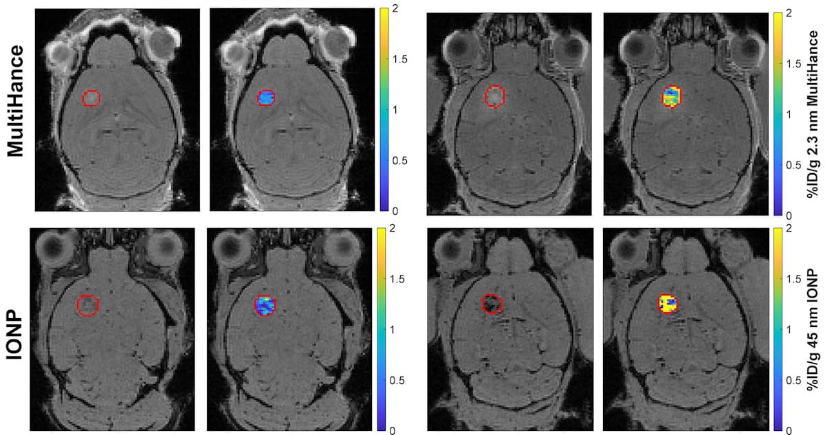
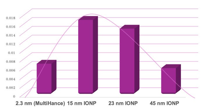
Brain tumour images Representative MR images of baseline (left panels) and FUS-treated (right panels) mouse brains. The top row shows administration of a 2.3 nm contrast agent (MultiHance), the bottom row shows administered iron oxide nanoparticles, 45 nm in size. Each pair of panels shows the anatomic image with the tumour outlined in red on the left, and the corresponding image superimposed with a concentration map showing the amount of nanoparticle retained within the tumour (as a percentage of the injected dose per gram) on the right. (Courtesy: CC BY 4.0/Radiology 10.1148/radiol.251005)

Drug delivery to the brain has been a longstanding challenge in medicine. One option is focused ultrasound (FUS), which can safely disrupt the blood–brain barrier for drug delivery. But how much of a drug gets into the brain depends heavily on its size. A long-standing assumption is that delivery decreases as drug size increases. But by using a clever spin on MRI physics, researcher Matthew Hoch and colleagues from the University of Virginia have shown that “the smaller the better” might not be entirely correct.

The blood–brain barrier is one of biology’s toughest engineering problems. Composed of a dense, tightly sealed layer of cells lining every blood vessel in the brain, the blood–brain barrier only lets nutrients and oxygen through and protects the central nervous system by blocking bloodborne pathogens. In doing so, however, it also blocks the delivery of drugs to the brain. Brain tumours compound this with their own blood–tumour barrier, further hindering drug delivery. For years, researchers have pondered how therapeutics could be delivered past these checkpoints; the answer may simply lie in the use of sound.

The process begins with the injection of gas-filled microbubbles into the bloodstream, where they circulate freely. Exposure to FUS then expands and contracts the volume of these microbubbles, creating a temporary, localized gap that pries the barrier open just long enough for drugs to slip through. Although the technique works, it is unclear how much of a drug actually comes through. In this new study, the team investigate how the size of the drug influences FUS-mediated drug delivery and introduce a novel technique to measure precisely how much drug is delivered.

The measurement problem

Many neurotherapies, with a range of sizes, could benefit from this drug delivery method. But measuring how much of the drug gets past the blood–brain barrier is challenging with current imaging methods. For example, fluorescence imaging is limited by its semi-quantitative nature, while PET scanning suffers from poor spatial resolution.

Standard MRI methods are not only time-consuming, but, in the form of T1-mapping, are typically limited by the size of commercially available contrast agents, which are small in comparison to larger neurotherapeutics used for immunotherapy and gene delivery. Other standard MRI methods sensitive to the presence of iron (T2-mapping) provide an alternative avenue to measure larger agents, but can again be limited by scan time for 3D visualization. Both approaches also have potential to suffer from low sensitivity at low concentrations.

Hoch and his team solve this measurement problem by introducing quantitative susceptibility mapping (QSM), an MRI technique with diverse applications in neuroimaging including evaluation of haemorrhage, iron deposition and calcification. QSM works by exploiting the distortion of local magnetic fields by different materials, a property called magnetic susceptibility. By injecting iron-based nanoparticles that induce measurable, spatially localized shifts in the MRI signal’s phase, QSM can generate a 3D map of magnetic susceptibility. This can then be used to calculate the actual concentration of iron-based nanoparticles within tissues.

By transforming an MRI scanner into a sensitive nanoparticle detector, the researchers present a novel way to quantify drug delivery down to fractions of a percent of the injected dose.

What did they find?

The team tested this approach using four different particles, with a 20-fold range in size. The first was a small gadolinium-based contrast agent, MultiHance (a proxy for small molecule therapeutics), at around 2.3 nm; the other three were iron oxide nanoparticles (IONPs) of 15, 23 and 45 nm, sizes that mirror the dimensions of therapeutic candidates used for immunotherapy and gene therapy.

Using healthy and glioma brain tumour-carrying mice, the researchers used FUS treatment to open the blood–brain barrier and deliver particles of varying sizes. They recorded MRI scans before and after delivery and used QSM to generate a precise measurement of how much of each particle made it into brain tissue.

Brain delivery by particle size
Brain delivery by particle size The amount of drug delivered, as a percentage of the initial injected dose, that has successfully travelled to the brain. (Courtesy: Adapted from Radiology 10.1148/radiol.251005/CC BY 4.0)

The results were unexpected. Drug delivery followed a bell-shaped curve in healthy mice. From the smallest (2.3 nm) particle to the 15 nm IONP, delivery increased 2.6-fold, then at 23 nm, remained steady. Interestingly, at 45 nm, delivery dropped by 2.5-fold compared with the 23 nm nanoparticle, comparable to that of the smallest agent.

This sweet spot, ranging from 15 to 23 nm, demonstrates that smaller isn’t always better. The researchers suspect that this trend in drug delivery is due to a balance between how easily a particle can squeeze through the barrier (so favouring smaller particles) and how long a particle stays in circulation, giving it more time to travel across the barrier (favouring larger particles).

In the mice with brain tumours, where there is an addition of the tumour’s own leaky, disorganized vasculature, the blood–tumour barrier, drug delivery can differ from that to healthy brain. Specifically, this barrier is thought to make drug delivery more difficult than in healthy tissue due to higher tissue pressures and inconsistent blood flow. But the researchers unexpectedly found that FUS boosted delivery of both small and large agents into tumours, with no real difference to the drug delivery levels seen in healthy brain tissue, despite the added presence of the blood–tumour barrier.

“The outcome is exciting because it means that focused ultrasound delivery performance is not expected to diminish in brain tumours,” says senior author Richard J Price in a press statement. “In fact, it may even be enhanced for some types of therapeutics.”

FUS-mediated barrier opening is currently in clinical trials for use in Alzheimer’s disease and glioblastoma, and this research has implications in both drug engineering and treatment planning. By introducing QSM, Hoch and his colleagues have provided a universal, precision technique to quantify contrast agent delivery. Taking existing tools, used for a specific physics measurement problem, and developing them to answer a completely different biological question is no small feat. Here, the researchers present an ingenious intersection of physics and biology, and its potential application in medicine.

The researchers report their findings in Radiology.

The post Breaking in: how ultrasound smuggles drugs past the blood–brain barrier appeared first on Physics World.

  •  
❌