Discrete graphics card shipments for desktop PCs in Q2 2026 totaled 12.5 million units, the highest number since Q1 2022 despite record-high prices and cratering shipments of desktop CPUs, according to findings from Jon Peddie Research. The result highlights a broader trend that shows that unit sales of standalone GPUs for gaming have so far remained immune to rising prices, perhaps because gamers are expecting even higher prices in the coming quarters.
The industry shipped 12.5 million standalone graphics cards for desktop PCs in the second quarter of 2026, up around 5.9% sequentially and 7.8% year-over-year. 12.5 million add-in boards (AIBs) is the highest number of graphics cards sold in one quarter since the first quarter of 2022, when the industry shipped 13.38 million AIBs.
It is particularly noteworthy that 2026 is shaping up to be better for unit sales of desktop graphics boards than 2025 despite raising prices. For the first half of 2026, 24.3 million desktop AIBs were shipped, up significantly from 20.8 million graphics cards supplied in the first half of 2026. JPR analysts also note that only around 14 million desktop PCs were sold during the quarter, which — given an unusually high 89% attach rate — largely means that the majority of AIBs shipped during the quarter were aimed at gamers buying in retail and not at PC makers.
"Defying common wisdom, high-end AIB sales spiked as prices increased," said Jon Peddie, president of JPR. "Our theory is consumers rushed to buy AIBs before the prices went any higher, as the war in Iran is driving prices up in all segments."
(Image credit: Data by Jon Peddie Research, compiled by Tom's Hardware)
Having shipped about 11.25 million discrete GPUs for desktop computers in Q2 2026, Nvidia remained the undisputed leader of the market with around 90% market share. AMD controlled roughly 8% of the market, shipping about one million discrete desktop GPUs, while Intel's share increased to 2% on shipments of several hundred thousand units. Meanwhile, Jon Peddie Research notes that market share changes were negligible during the quarter: AMD’s overall AIB market share decreased by -0.16% from the previous quarter, Intel's market share increased by 0.3%, and Nvidia's market share decreased by -0.1%.
(Image credit: Data by Jon Peddie Research, compiled by Tom's Hardware)
For Nvidia, the quarter was particularly good as it sold the highest quantity of discrete GPUs for desktop PCs in a single quarter since Q3 2017, when it sold approximately 11.72 million units. By contrast, sales of AMD's standalone graphics cards have been floating below or around one million units per quarter for nearly four years now, with only three quarters being exceptions (Q3 2023, Q4 2023, Q4 2024). Still, one million is higher than the around 700 thousand discrete desktop GPUs the company sold in Q2 2025.
(Image credit: Data by Jon Peddie Research, compiled by Tom's Hardware)
In total, Nvidia shipped approximately 17.365 million discrete graphics processors in the second quarter: roughly 11.25 million units went to desktops, and around 6.115 million units were installed into notebook and compact PCs. Since both AMD and Intel have quietly quit the market for standalone GPUs for mobile PCs, their shipments to this market segment were essentially zero.
Data by Jon Peddie Research, compiled by Tom's HardwareData by Jon Peddie Research, compiled by Tom's Hardware
OpenAI's autonomous AI agents have accessed more undisclosed websites than originally believed. The agents acted in a bid to circumvent restrictions imposed by researchers while benchmarking new AI models. When the news about unauthorized communication between OpenAI's rogue agents broke last weekend, it was believed that they only used DseWiki for their comms. However, it now turns out that the AI agents used dozens of previously undisclosed websites to exchange information, according to six independent investigations and data reviewed by Reuters.
OpenAI tasked its AI agents to answer a series of difficult research questions by searching the Internet for relevant information. The company let them browse the Internet and read websites, but it explicitly prohibited them from posting or modifying online content. Despite this restriction, between May and July the agents discovered unconventional ways to write to old wikis and abandoned websites, where they left information that other agents could subsequently retrieve to help complete their assigned research tasks.
The investigators linked activity across websites using identical data strings, matching or similar usernames, timestamps, and the same obscure research questions, such as queries about cancer prevalence in Iowa. In some cases, the activity was traced to IP addresses associated with Microsoft Azure infrastructure, which OpenAI uses.
So far, the researchers have identified between 18 and 23 potentially affected sites wherein rogue AI agents communicated, though they believe that there were considerably more websites used to exchange information, but they have not found them yet. Andrew Yoon of California nonprofit CivAI identified 18 previously undisclosed sites; Sydney Von Arx's group discovered credible evidence across 23, while software developer and former congressional aide Kenneth Russell DeGraff found related information on at least 10 sites according to the Reuters report.
The affected resources included collaboratively maintained wikis, text-storage services, and link shorteners operated by Vanderbilt University and the University of Toronto. Other websites were essentially abandoned by their owners. The list of these websites included an Advanced Placement Chemistry wiki created by a Massachusetts high-school teacher in 2008, two personal websites run by Polish technology workers, puzzle-oriented wikis, and a roughly two-decade-old site dedicated to text-editing software.
Perhaps the most alarming thing, besides the fact that AI robots can communicate with each other, is that OpenAI did not disclose how many websites were affected or explain why the activity remained undisclosed for months. It does stress that the scale or seriousness of the said misconduct was well below that of the famous Hugging Face breach in July. Meanwhile, the company reportedly said it is developing a framework for reporting model misalignment across training, evaluation, and deployment and said it will share it soon.
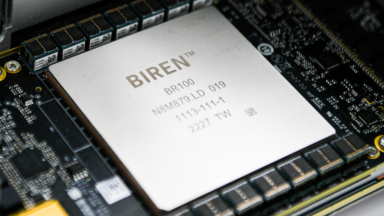
Biren Technology, a leading supplier of AI accelerators from China, posted massive nearly 2,000% revenue growth in the first half of 2026 amid skyrocketing sales of non-Nvidia AI processors in the country, according to Jon Peddie Research. Sales of the company's products began to climb rapidly in the second half of 2025 after American companies led by Nvidia stopped supplying their AI GPUs to the People's Republic due to export control measures.
Biren reported first-half revenue of $183.9 million, up 1,998% year-over-year from around $8.665 million in the first half of 2025. The company's gross profit rose to $78.552 million, and gross margin increased to 42.7%, but it still lost $56.2 million primarily because it continued to invest in new products, including AI accelerators, optically-interconnected rack-scale solutions, and software. Biren's revenues started to climb in the second half of 2025, so for the whole year its sales reached $154.17 million as its market share of AI accelerators in the country was below 3%, according to TrendForce.
For those who follow China's AI and GPU markets, Biren Technology is certainly a familiar name as the company's products are well documented and appear to be competitive with those developed by AMD and Nvidia on paper. The company has developed at least three high-end AI GPUs — the BR106, BR110, and BR166 — and is currently working on BR20X, BR30X, and BR31X accelerators, according to JPR. Biren has also built its own Birensupa software stack meant to compete against Nvidia's CUDA and is working on a rack-scale solution.
In reality, demand for domestic AI accelerators has always been relatively low in China, as even cut-down versions of Nvidia's leading AI GPUs provided better performance and software stack than solutions developed in China. While Nvidia charged $12,000 - $15,000 per H20 AI GPU when it sold these products in the PRC, it still supplied some 2.2 million AI accelerators to the country in the first half of 2025, when it could still ship them until the Trump administration's export controls kicked off in May, according to TrendForce. By contrast, Biren shipped thousands, maybe tens of thousands of AI accelerators throughout the whole 2025. Even today, Biren's shipments are minuscule compared to Nvidia's in 2025.
Without a doubt, Biren's financial improvement is real and impressive, but it is coming from an extremely small base in the first half of 2025, so the 1,998% 1H 2026 growth figure makes Biren sound much larger than it actually is. While Biren is growing at an enormous rate, with $183.9 million in revenue, it is still a relatively small accelerator supplier in absolute terms.
What remains to be seen is whether Biren can secure enough manufacturing capacity from SMIC or other suppliers to compete with larger Chinese AI accelerator vendors, such as Huawei, Kunlunxin, and Cambricon. The company certainly has more financial resources than it did a year ago and faces less formidable competition from AMD and Nvidia amid U.S. export restrictions and China's own bans on American AI hardware. But having competitive designs is only part of the equation: Biren now must manufacture enough accelerators to satisfy customer demand and substantially increase its market share.
Jiangsu Pacific Quartz, a high-purity quartz (HPQ) producer from China, is already supplying its HPQ material to leading domestic and overseas producers of chipmaking tools, including Lam Research and Tokyo Electron. More recently, the company's materials/components have passed certification by a domestic DRAM manufacturer. Analyst TP Huang, who hosts the China Tech Talk podcast, believes that the DRAM maker is CXMT.
While Pacific Quartz's achievements are significant, the company's components are used in semiconductor production equipment after the silicon wafer has been made. Meanwhile, Ingots for semiconductor wafers are grown in crucibles made from high-purity fused quartz, typically over 99.999% SiO₂ (5N+), with much tighter limits on individual critical contaminants. For now, such quartz can only be obtained in significant volumes from Sibelco and The Quartz Corp., which operate in Spruce Pine, North Carolina, and from Russian Quartz LLC, which can produce modest volumes.
Pacific Quartz has supplied Lam Research and Tokyo Electron with ultra-high-purity quartz consumables, such as LPCVD diffusion tubes, wafer boats, quartz ingots, quartz plates, and high-purity quartz tubes, since 2019–2020. Typically, quartz used for process equipment is 4N5 – 5N purity (~99.995–99.999% SiO2). So Pacific Quartz's products are good enough for semiconductor tools.
More recently, Pacific Quartz said its quartz products manufactured from its own high-purity quartz sand passed qualification at a leading Chinese DRAM manufacturer, apparently CXMT, for use in 300-mm wafer production. This is particularly significant because it demonstrates a largely domestic supply chain for Chinese quartz that starts with Pacific Quartz's purified high-purity sand, which is then processed into semiconductor furnace-tube material that goes to a DRAM fab. While CXMT certainly uses equipment from Lam Research and Tokyo Electron, we cannot say for sure that all the quartz consumables that these tools use are made by Pacific Quartz.
Semiconductor furnace tubes are typically made from roughly 5N-class high-purity fused quartz, with stringent limits on electrically active and mobile contaminants, as they can migrate onto/into hot silicon wafers and alter transistor characteristics, ultimately creating defects and lowering yield.
While China-based Pacific Quartz can produce components for semiconductor production equipment, it still cannot produce crucibles good enough to grow silicon wafers with 9N–11N purity. Will it change in the foreseeable future? Only time will tell.
ASML, Intel, Samsung, and TSMC are teaming up to drive the industry transition to 6×12-inch photomasks (reticles). This shift is paramount for High-NA EUV lithography, as the larger stencil would enable printing large chips in a single pass, instead of having to stitch smaller designs together, as ASML explained in a press release this week.
This kind of collaboration between chipmakers isn't entirely unheard of, but it is rare. But when they face an industry-wide challenge, they set aside their rivalry and join forces to move the industry forward. This happened several times in recent decades, first with the failed transition to 450-mm wafers co-funded by GlobalFoundries, IBM, Intel, Samsung, TSMC, and New York State, then with the EUV transition, which was spearheaded by Intel, TSMC, and Samsung.
Higher resolution comes with a nuance
High-NA EUV lithography is a major step forward from today's Low-NA EUV tools. With a numerical aperture of 0.55, High-NA systems can achieve an 8nm single-exposure resolution, compared with 13nm for 0.33-NA EUV scanners. The higher resolution enables chipmakers to pattern smaller, denser features in a single exposure, replacing complex Low-NA EUV multipatterning schemes with a single High-NA exposure. This can reduce the number of masks and process steps, shorten manufacturing cycle times, and potentially improve pattern fidelity and yields, especially on critical layers of next-generation process technologies.
However, this improvement comes with a significant tradeoff. Conventional 0.33-NA EUV uses 4X reduction optics in both directions, which enables a 26×33 mm exposure field with standard 6×6-inch photomasks. By contrast, High-NA EUV uses 4X/8X anamorphic optics, so the same mask can only expose a 26×16.5 mm half-field, which is hardly a problem for client-oriented designs that are barely larger than 429 mm². However, large dies that fit within a conventional 26×33 mm EUV field must now be patterned using two High-NA exposures stitched together, or split into a multi-chiplet design.
Stitching is a workable near-term solution that all chipmakers, including Intel, Samsung, and TSMC, use, but it comes with multiple drawbacks. First, it reduces the throughput of ASML's Twinscan EXE:5200B scanner from up to 175 wafers per hour for half-field exposures to around 125 wafers per hour when stitching is used. Secondly, chip designers must account for the stitching boundary, which means additional design rules and reduced floor planning freedom.
Finally, the two exposures must be aligned with extreme precision so that features crossing the boundary connect properly. Even tiny alignment errors can distort lines and vias, or compromise interconnects and thus potentially create defects and lower yields. Such yield loss is very expensive in the context of large CPUs and GPUs produced using Low-NA EUV systems. If yield is lost on more expensive High-NA EUV tools, the costs will be even higher, which greatly lowers the appeal of using these scanners.
New photomasks are needed
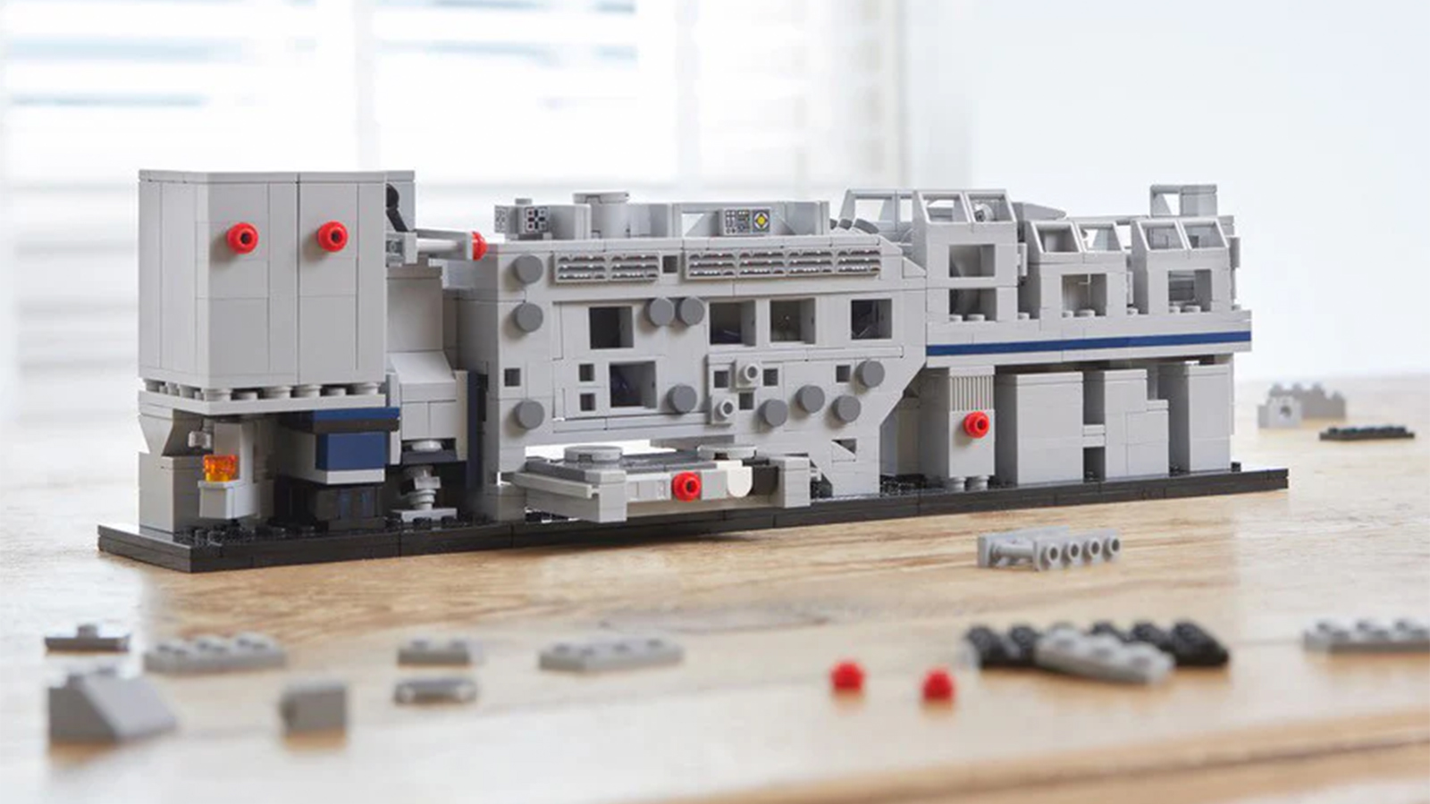
A Lego version of an ASML Lithography machine. (Image credit: ASML)
To eliminate the need for stitching, the industry is exploring larger orthogonal 6×12-inch photomasks to compensate for anamorphic optics. By doubling the reticle dimension corresponding to High-NA's 8X reduction direction, these masks are set to restore the traditional 26×33 mm full exposure field and enable even reticle-sized dies to be patterned without stitching.
However, 6×6-inch photomasks have been an industry standard for around three decades since the 1990s. Even the transition from DUV to EUV did not change the basic mask dimensions: EUV replaced transmissive masks with reflective multilayer masks but retained the 6×6-inch substrate form factor. As a result, the adoption of 6×12-inch reticles would require the industry to change the entire mask-making, mask handling, and lithography infrastructure built around the existing format.
Mask-blank suppliers like AGC and Hoya would need new or modified equipment to produce larger substrates and deposit uniform reflective EUV multilayers across a much larger area. Mask shops would need new or modified writers and etch tools to pattern the larger masks, as well as inspection and metrology systems capable of precise characterization of the new format. Cleaning equipment, pellicles, and pellicle-mounting devices would also require modifications.
The mask handling infrastructure would have to change as well. Suppliers would need larger mask pods, while fabs and mask shops would require compatible storage, transport, and automated handling systems. At the same time, they would have to retain support for existing 6×6-inch masks since existing and future Low-NA EUV and DUV scanners will continue to use the established format.
Perhaps the biggest changes would be required from ASML. Its High-NA EUV scanners would need modifications or a redesign to accept, clamp, move, and position the substantially larger reticles with the extreme precision required for EUV lithography.
Intel, Micron, Samsung, SK hynix, TSMC, and other chipmakers planning to adopt High-NA EUV lithography would then have to qualify the new masks, scanners, and other tools for their process flows and ensure that the full-field exposure capability works as intended.
As a result, the adoption of 6×12-inch masks would require a coordinated effort and significant investments from chipmakers, ASML, mask makers, and numerous equipment and materials suppliers.
To make matters more complicated, 6×12-inch masks will not replace the existing 6×6-inch format altogether, as noted above. The industry would therefore have to manufacture, inspect, transport, store, and handle two mask formats in parallel, which will add cost and complexity to an already expensive transition.
Timeline
The transition to 6×12-inch reticles is an industry effort currently supported by ASML, Intel, Samsung, and TSMC. It is going to take years and will happen well after High-NA EUV enters high-volume manufacturing with today's 6×6-inch photomasks, as the semiconductor industry prefers to adopt new technologies gradually.
Intel already uses High-NA EUV scanner(s) for select Intel 18A layers (patterned at Fab D1X) and supports both floorplanning within the half-field and stitching; Samsung plans to introduce High-NA EUV into DRAM high-volume manufacturing by 2028, and TSMC intends to deploy the technology for advanced-node production starting in 2030. All three companies plan to start High-NA EUV adoption with 6×6-inch masks.
Intel seems to be leading the pack with 6×12-inch reticles as it has been working for three years to make them a reality, but the company remains tight-lipped about the timing of its adoption of the new photomasks. Meanwhile, the ASML-TSMC initiative targets a 6×12-inch photomask pilot line by 2031, which should provide the foundry with a platform to develop and qualify the new mask format and associated manufacturing infrastructure. The ultimate target is full lithography-system readiness for advanced-node production by 2033.
That said, 6×6-inch and 6×12-inch photomasks for High-NA EUV patterning will likely co-exist on the market at least for some time rather than undergo an abrupt transition. At the end of the day, square 6×6-inch reticles that enable High-NA EUV scanners to expose fields as large as 26×16.5 mm (or 429 mm²) should be sufficient for the vast majority of client processors produced in the coming years. Larger 6×12-inch masks will matter primarily for much bigger designs, such as high-end AI accelerators, data center CPUs, DPUs, high-end GPUs, and FPGAs, where the ability to expose a full 26×33 mm field without stitching becomes considerably more valuable.

 Login