Intel is set to raise $19.7 billion by selling new common stock in a bid to finance the building out of new production capacity, the development of next-generation leading-edge process technologies like 14A and others, and day-to-day operations. While the company does not assign money to a particular project, Intel needs to build capacity to land orders from large external clients, so capacity expansion will likely be a priority. According to Bloomberg, the share sale attracted $100 billion in demand.
Intel will sell 210,526,315 shares for $95 apiece through an underwritten public offering. In addition, participating banks have 30 days to acquire as many as 31,578,947 more shares at the same $95 price, minus applicable underwriting discounts. Should they exercise all their options, Intel could sell approximately 242.1 million shares altogether and increase the proceeds to roughly $23 billion. Without the additional shares, Intel expects net proceeds of approximately $19.7 billion after underwriting discounts, commissions, and estimated expenses. The transaction is scheduled to close on August 12, 2026.
Intel's market capitalization increased from roughly $90 billion last August to $491 billion at press time, so the time is right to sell some shares and raise some much-needed cash, as the company must compete against giants like TSMC and Samsung, which spend tens of billions of dollars every year on new fabs and advanced process technologies. Meanwhile, Intel's capitalization reached its all-time high of $673 billion on June 20, 2026.
Intel has not assigned the money it is going to raise to particular projects and says the capital can be used across the business, including for capital expenditures and working capital. The company is currently ramping up its Fab 52 in Arizona and is on track to start using adjacent Fab 62 when it needs to. In addition, the company still has to build its fab complex in Ohio, which is expected to cost over $100 billion when fully built, so it badly needs money.
In its risk disclosures, the company specifically mentioned Intel 14A — which is due to enter mass production in 2028 — and other advanced process technologies, manufacturing expansion required to support them, and the need to secure design wins and volume commitments from major external foundry customers. While Intel does caution that these long-term investments amounting to tens of billions may not generate adequate returns, it is impossible to land sizeable contracts from external customers without having production capacity readily available.
Interestingly, Intel also mentioned alternative financing arrangements, government grants, and the U.S. government's significant equity position in the company among relevant factors.
House Select Committee on China Chairman John Moolenaar has written a letter that demands the U.S. government enforce an existing export control measure designed to prevent Chinese companies from getting advanced chips produced by contract chipmakers like TSMC or Samsung Foundry.
When Joe Biden was about to leave the office in early 2025, he signed a law that required chipmakers to determine their end customers in a bid to prevent contract manufacturers from unknowingly fabricating chips using American technologies for companies that served as intermediaries for restricted organizations tied to the Communist Party or the People Liberation Army. The regulation was introduced after it was discovered that chips made by TSMC for China-based Sophgo were actually Huawei's Ascend 910B AI accelerators. However, the Trump administration announced in May 2025 that it would not enforce this semiconductor regulation known as the 'Foundry Due Diligence Rule,' which naturally created uncertainty about whether the foundry-focused requirements would be actively implemented at all.
"The announcement created ambiguity as to whether front-end fabricators like TSMC can export unpackaged advanced dies to non-approved designers located outside of China, without performing the due diligence specified in the Foundry Due Diligence Interim Final Rule (IFR)," the letter reads. "These exports enabled Huawei to obtain millions of controlled Ascend logic dies from TSMC, using its front company, Sophgo in 2023 and 2024."
Before the adoption of the 'Foundry Due Diligence Rule,' Chinese companies and/or their intermediaries could misrepresent chip specifications and end users when placing orders with TSMC or other foundries, which allowed restricted devices to be made despite U.S. export controls. Under the rule, foundries and OSAT providers exporting chips produced on 14/16nm-class process technologies or more advanced nodes must presume those devices qualify as controlled AI processors subject to a global licensing requirement, unless they meet an exemption. According to the letter, foundries have generally complied with these requirements since the rule took effect. As a result, Moolenaar essentially asks the government to enforce the existing controls rather than introduce stricter export controls.
Moolenaar believes that the Commerce Department's Bureau of Industry and Security could clarify its current stance on the Foundry Due Diligence Rule in two ways:
By issuing guidance, which confirms that the worldwide Regional Stability (RS) licensing requirement still applies to exports from front-end foundries;
By formally annulling the AI Diffusion IFR and amending §744.23 to explicitly restore that requirement for both foundries and OSAT providers.
Either approach would eliminate conflicting interpretations and reinforce enforcement of existing export controls, Moolenaar believes.
Nvidia late on Monday announced that it had signed memorandums of understanding with Apollo, BlackRock, Blackstone, Brookfield, Goldman Sachs, and KKR to establish independent financing platforms that could mobilize more than $500 billion in third-party capital to invest in AI infrastructure. Nvidia's goal is to ensure that its clients building AI data centers (which Nvidia calls AI factories) can get enough money from powerful financial companies. As a result, Nvidia will reinforce its position on the AI hardware market as the funds will exclusively finance Nvidia-based AI data centers.
The proposed funds (or platforms, as Nvidia calls them) are intended to provide dedicated pools of capital for customers — such as AI labs, cloud service providers, or enterprises — that deploy Nvidia-based infrastructure. Rather than financing projects itself, Nvidia intends to work with six investment firms to enable access to long-term funding at attractive rates. The company believes that AI infrastructure should not be viewed as conventional IT equipment, but as tools that make sustained economic returns, which is why it must be financed appropriately.
"We are in a pivotal moment of a historic AI investment cycle," said David Solomon, Chairman and CEO of Goldman Sachs. "Nvidia's full-stack platform is in high demand and uniquely positioned at the center of that global buildout. Our investment and distribution roles reflect our confidence in Nvidia's leadership, and we are excited for the new opportunity to create a market for credit backed by NVIDIA compute."
The financial companies believe that AI data centers can be treated as long-duration infrastructure assets rather than conventional IT equipment, in part because Nvidia compute can generate revenue over an extended period and retain value across different workloads and operators. As a result, they appear to believe that AI infrastructure can support long-term financing at attractive rates, although the companies do not explicitly claim that financing AI data centers carries lower credit risk than financing conventional IT deployments. Furthermore, it should be noted that Nvidia and financial companies will inevitably finance companies that would otherwise struggle to obtain capital to finance their AI data centers. This will ultimately help Nvidia sell more hardware and software while allowing its financial partners to capitalize on the rapid expansion of Nvidia's AI ecosystem.
Without any doubt, the arrangement will help to rapidly build AI infrastructure, which will increase adoption of AI technologies. However, this arrangement increases the risk of an AI infrastructure bubble as it potentially weakens one of the natural brakes on overbuilding: the availability and price of capital. Furthermore, Nvidia's help with arranging financing for its own customers introduces an element of circular financing into the AI boom, something that the industry faced during the dot-com bubble era in the late 1990s – early 2000s. However, this does not necessarily prove there is a bubble, as there is genuine, enormous demand for AI hardware and Nvidia sells plenty of such hardware.
Perhaps the biggest concern about the arrangement is that while Nvidia and its partners state that AI infrastructure can provide long-term value, AI accelerators, such as Nvidia's GPUs, have short and uncertain economic lives as the company and its industry peers introduce new and better-performing AI hardware every year, which devalues the previous generation.
"Nvidia has reached an important milestone: we began by building chips; today, we are helping create a new class of productive, investable infrastructure: AI factories," said Jensen Huang, founder and CEO of Nvidia. "In AI, compute is revenue. Nvidia compute is uniquely suited for this role. It is broadly adopted, flexible across models and workloads, fungible and transferable across customers and operators, and continuously improved through CUDA software — extending its useful life and improving its economics over time. It is supported by a deep global ecosystem of developers, customers, and offtakers. That is why we are bringing the world's leading long-term capital providers together to independently underwrite AI infrastructure. These financing platforms will help customers access scarce compute at scale and build the DSX AI factories that will power every industry and country in the age of AI."
Apple used to be among a few companies willing to buy memory and other components worth billions of dollars under long-term supply contracts at fixed prices. But the artificial intelligence era represents a new reality with new purchasing champions, marking a tectonic shift in the high-tech world. Alphabet, Microsoft, Meta, and Amazon have purchase commitments totaling about $2 trillion, and a significant portion of these commitments are for memory, according to estimates by analyst Claus Aasholm. While the commitments are approximate, span many years, and should be generally taken with a grain of salt, they still reflect the direction the industry is moving.
Combined purchasing commitments from the four major hyperscalers shown in the chart —Amazon, Alphabet, Meta, and Microsoft — reached nearly $2 trillion by Q2 2026, with Alphabet and Microsoft accounting for the overwhelming majority of the total.
The rapid expansion suggests several major findings. Firstly, the AI infrastructure race is accelerating, not stabilizing. Secondly, AI infrastructure investments are driven by a handful of hyperscale cloud service providers (CSPs) whose long-term procurement commitments now vastly exceed those of traditional consumer electronics companies such as Apple.
Thirdly, memory has become a strategic asset — perhaps a competition weapon — rather than a commodity. Fourthly, suppliers of memory — both 3D NAND and DRAM — are gaining pricing power. Finally, demand for memory will likely drive major capacity expansion at Micron, Samsung, and SK hynix, even though so far these companies have been exceptionally disciplined about their capacity investments.
Almost $2 trillion commitments
Google shows by far the most aggressive increase in purchasing commitments, rising from roughly $140 – $150 billion in Q3 2025 to around $811 billion by Q2 2026 (though these are total purchase commitments by Alphabet, not specifically memory purchase commitments), while Microsoft follows a similar trajectory and reaches approximately $678 billion in total obligations, which includes, but is not limited to memory.
Meta is also ramping commitments substantially to around $349.3 billion (again, these are total commitments), whereas Amazon increased its commitments more gradually to roughly $130 billion. By contrast, Apple — which makes the world's most popular smartphone, and which was the largest consumer of memory just a couple of years ago — remains almost flat throughout the period at approximately $57 billion (of which $56.2 billion is payable within 12 months). Apple's commitments fall well short of Nvidia's commitments of $119 billion.
Memory suppliers used to buzz around Apple like fruit flies, but now they have discovered larger commitments.Apple's purchasing commitments have not changed, suggesting a reluctance to follow the new market rules.https://t.co/0pRbk8aYVJ pic.twitter.com/t2VNm7uw1dAugust 6, 2026
Again, we are talking about total purchase commitments, which include foundry capacity, 3D NAND, and DRAM memory, but are not limited to them. Alphabet, Amazon, Meta, and Microsoft all build custom silicon and custom servers, so a significant portion of these commitments is to various EMS providers.
While $1.968 trillion of purchase commitments for memory and storage alone would be an absurdly large amount of money, a huge portion of these commitments consists of contract manufacturing obligations as well as memory chips. This suggests that the foundry, 3D NAND, and DRAM markets are entering a new phase in which hyperscalers are willing to make vastly larger forward purchasing commitments than traditional consumer-electronics companies, giving suppliers a strong incentive to prioritize customers prepared to secure future capacity on that scale.
Strategic assets
While Claus Aasholm's chart is explicitly dedicated to memory, it does describe total purchase commitments of tech giants, so the chart can reasonably be read as evidence that memory and capacity at TSMC, Samsung Foundry, and GlobalFoundries are becoming a strategic asset rather than merely another component to procure at the best available price.
AI infrastructure requires enormous quantities of AI accelerators, DRAM (including HBM), and 3D NAND. Meanwhile, the supply of high-end memory (HBM) is constrained by fab capacity at major DRAM makers, whereas the supply of AI accelerators is constrained by both wafer capacity and foundries and packaging capacity at foundries and their OSAT partners. As a result, hyperscaler CSPs have an incentive to lock in supply years ahead, even if doing so requires exceptionally large purchasing commitments.
That also changes the relationship between semiconductor suppliers and their customers. In theory, a company willing to guarantee hundreds of billions of dollars of future purchases can effectively help underwrite expansions of foundry, memory, and advanced packaging capacity and, in return, secure priority access to scarce products and future process technologies. In reality, TSMC can well afford capacity expansion using the money it gets from hyperscalers and give priority to its largest customers. In this environment, access to DDR5, HBM, and 3D NAND memory becomes part of the competitive advantage rather than merely a procurement exercise.
This is also what makes Apple's position in the graph interesting: its purchasing commitments barely move while those of Alphabet, Amazon, Meta, and Microsoft surge. If the trend continues, Apple may remain one of the world's largest semiconductor buyers in absolute terms, but the question is whether it will be among the key customers that foundries, memory makers, and OSATs plan their future capacity expansions.
An inflection point
Perhaps the most interesting takeaway of the findings revealed by long-term purchase commitments is that the industry's center of gravity appears to have shifted.
During the smartphone era, foundries (well, TSMC has won) and memory suppliers often competed aggressively for Apple's business because of its enormous purchasing power. Today, hyperscalers building AI infrastructure are making purchasing commitments that dwarf those of traditional CE companies like Apple, which may well represent a strategic inflection point akin to the one Andy Grove described in his 'Only the Paranoid Survive' book.
Will this tectonic shift result in prioritization of customers capable of enabling future capacity expansions through massive long-term purchase agreements, or will foundries and memory makers remain more or less disciplined with their capacity expansions so as not to lose a lot when demand declines? This is a question that has yet to be asked.
In any case, the AI megatrend has transformed semiconductors — from foundries to advanced packaging and from DDR5 to HBM4 — into strategic assets that can no longer be treated as ordinary components procured on demand. And this is something that will continue in the long run.
SpaceX and Tesla on Thursday formally unveiled plans for the initial phase of their Terafab project. The first stage of the plan — which is expected to use Intel's 14A process technology — is expected to require $16.8 billion in investment, while the completed campus is planned to encompass more than 100 million square feet of manufacturing space. The massive semiconductor manufacturing complex will be built in Grimes County, Texas, at a location that belongs to SpaceX.
According to SpaceX and Tesla, their combined demand for semiconductors is projected to exceed 1 terawatt (TW) of compute per year, which significantly exceeds today's global supply. In fact, SpaceX, Tesla, and xAI already consume a significant portion of contract chipmaking services available today, and can potentially justify building a dedicated fab that will exclusively serve Elon Musk's companies. In particular, Terafab is envisioned to exclusively produce AI inference processors for Tesla Optimus humanoid robots and Cybercab autonomous vehicles, as well as 'high-power' processors intended for SpaceX's space-based data centers. Meanwhile, SpaceX and Tesla have not disclosed when their combined demand for compute per year will hit the 1 TW benchmark.
Unlike a conventional semiconductor fab, Terafab is envisioned as a vertically integrated manufacturing campus where advanced logic devices, memory chips, packaging, and testing operations are housed together. Normally, logic and memory are produced at different fabs using different process technologies, whereas packaging and testing services are performed at different facilities. However, the companies believe that consolidating logic, memory, packaging, and testing in one location will not only shorten the production cycle but will also shorten time-to-yield by enabling faster iterative improvements.
Given the description and the goal of the project, this will be a massive facility. Yet, SpaceX and Tesla have said little about its capabilities; The only thing they have disclosed is that the current facility in Grimes County will feature '100 million square feet of manufacturing space.' The 100 million square feet (9.3 million square meters) figure immediately stands out because it is far beyond anything ever announced for a semiconductor manufacturing facility. For example, the total area of Samsung's Pyeongtaek campus is approximately 2.89 million square meters, or 31.1 million square feet. A single Samsung fab occupies about 120,000 square meters, or 1.29 million square feet. However, the key wording is important: '100 million square feet of manufacturing space' does not mean 100 million square feet of cleanroom space.
Based on an image published by SpaceX, the Terafab facility will occupy four massive buildings. It is unclear whether these buildings will be four phases of the project (i.e., logic, memory, and packaging will be made under one roof) or will serve different purposes (i.e., one building makes logic, another produces memory, yet another does testing and packaging). In any case, when fully built, Terafab will be a massive semiconductor production campus that will require significantly more than $16.8 billion.
The announcement claims that the Terafab facility will employ at least 3,000 people, and that between 60% and 80% of them will be Grimes and nearby Brazos County residents.
Terafab is expected to use water from Gibbons Creek Reservoir instead of local groundwater and feature on-site wastewater treatment as well as water recycling and conservation measures.
The announcement follows Tesla's groundbreaking earlier this year on a research semiconductor facility at the North Campus of Tesla's Giga Texas campus, which the companies describe as a precursor to Terafab.
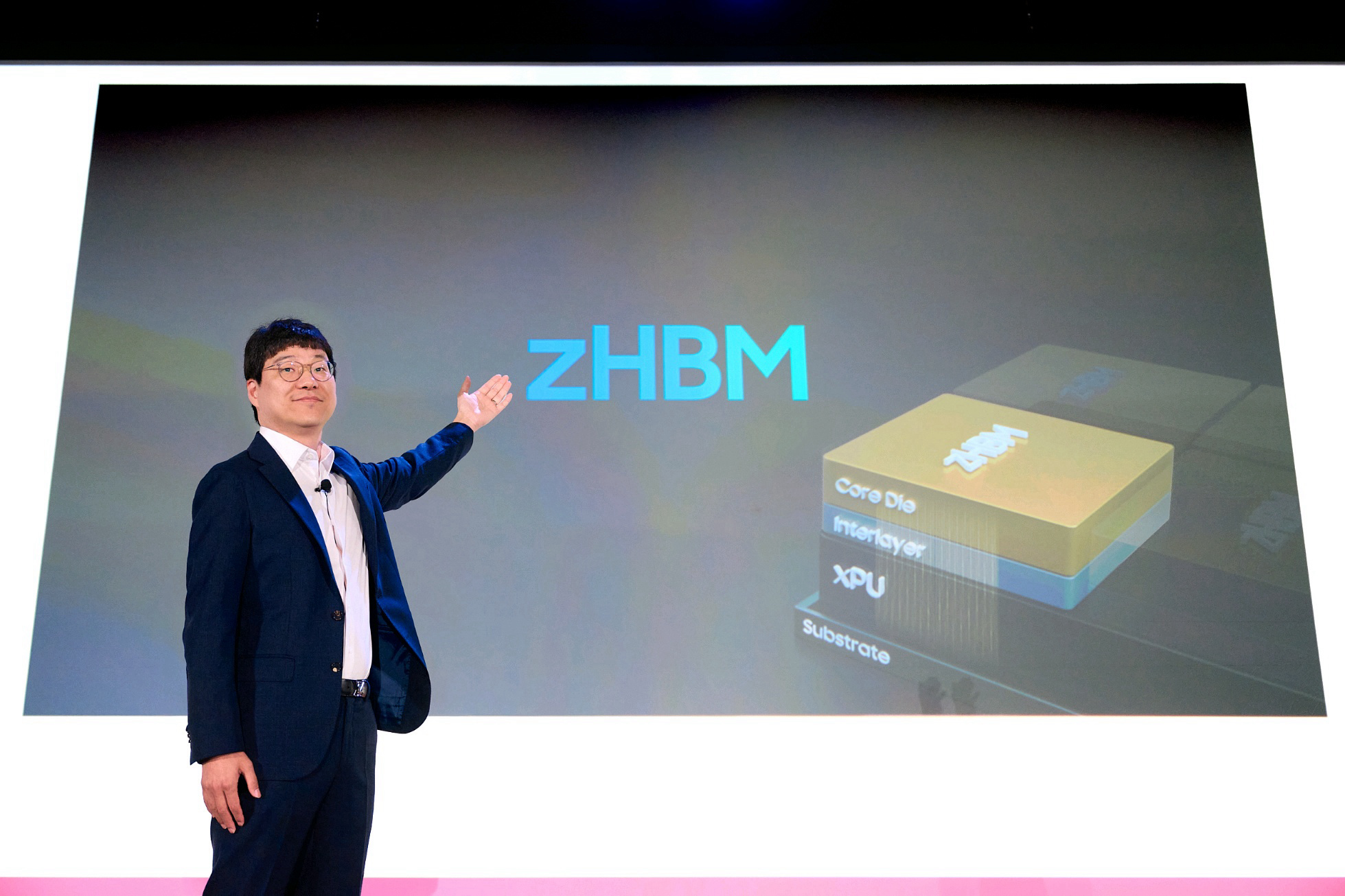
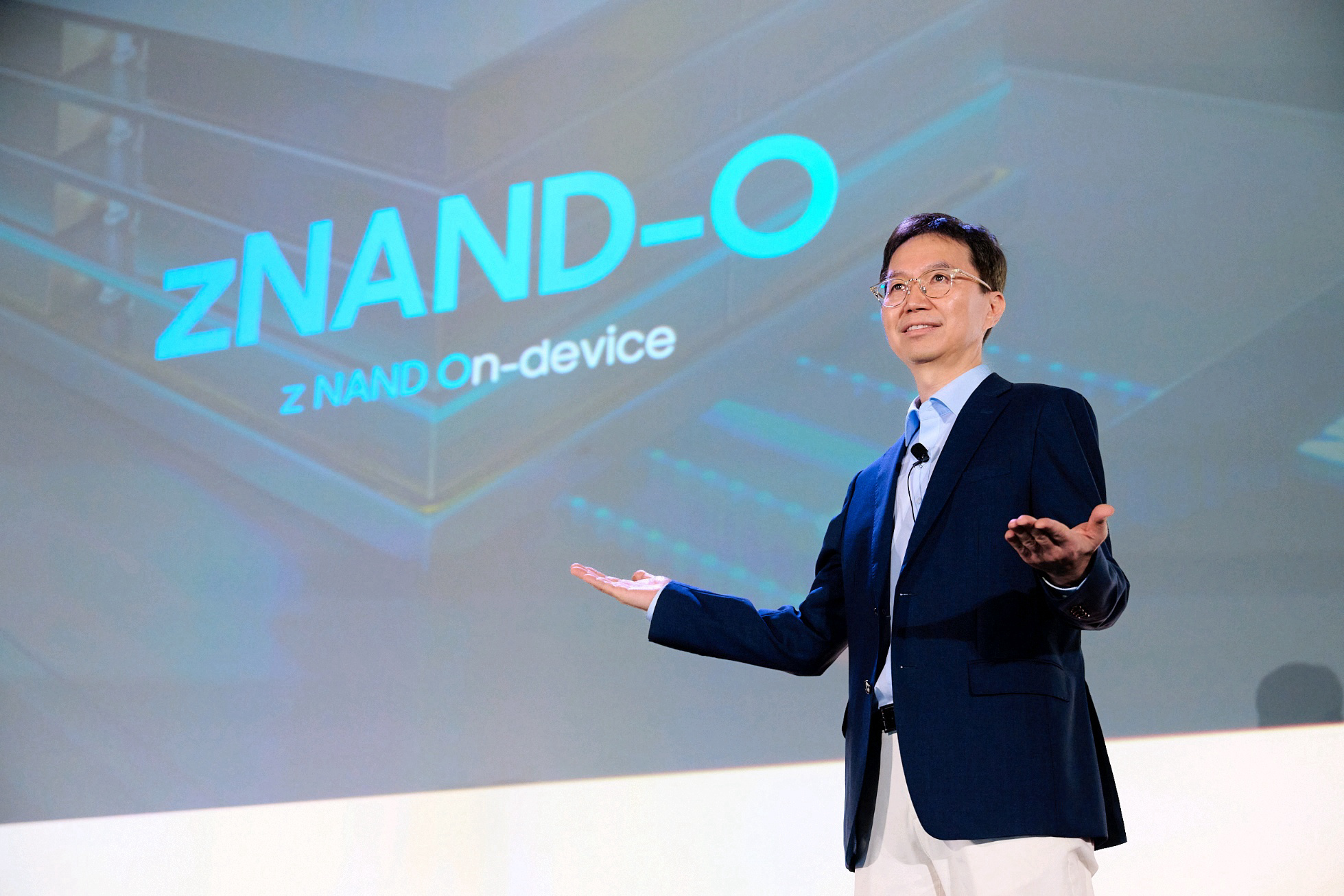
This week, Samsung presented its vision for next-generation memory and storage solutions both for AI and general-purpose applications at the Future of Memory and Storage (FMS) 2026 conference. The company introduced zHBM, zNAND-O, and BV-NAND technologies at the event, and while they are aimed at very different applications, they share one common ingredient: they all rely on wafer bonding.
Here's a breakdown of each type of technology that the company announced.
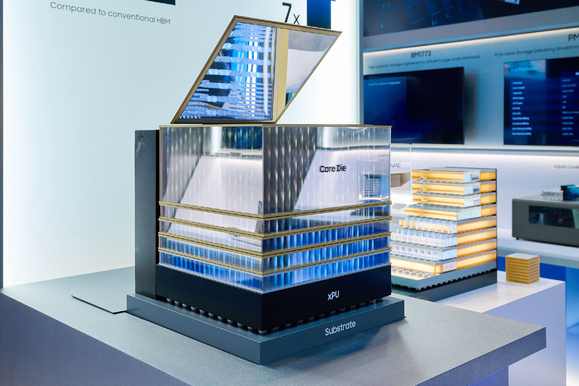
zHBM: Samsung’s vision for custom HBM ultra-high-performance memory that will sit on top of logic dies.
zNAND-O: NAND memory that can be bonded atop a logic device to maximize bandwidth, reduce latency, and minimize power consumption.
BV-NAND (aka Samsung’s 10th Generation V-NAND): Samsung’s take on bonding NAND arrays atop all the circuitry needed to operate them. This is essentially next-generation 3D NAND technology that is used today by almost everyone, including Kioxia/Sandisk, SK Hynix, and YMTC (which was the first company to adopt such a method).
This article is a preview of the type of content that readers can expect from our subscription service, Tom's Hardware Premium. If you're interested in more technical content that spans across the hardware industry, subscribe for as little as $29 per year, or $7 per month.
Don’t miss out on this Tom’s Hardware Premium. Get a full year of access for just $29, or from $7 per month. Get daily news analysis, deep dives into specialist topics in the semiconductor industry, as well as access to Bench, the largest benchmarking database around.View Deal
zHBM: Placing HBM stack on top of logic
Around the time we first heard about HBM4's 2,048-bit interface, we read a 'semi-official' report that SK hynix and its partners were considering vertical integration of HBM4 stacks on top of logic chips. To a large degree, companies were considering installing these memory stacks on top of their processors as they doubted that it would be possible and feasible to use interposers to connect HBM4 stacks to AI accelerators. Over time, it turned out that integration of memory on top of logic is complicated when it comes to cooling, power delivery, and developing interposers that can handle a 2,048-bit memory interface. Samsung's zHBM appears to be a continuation of that effort.
(Image credit: Samsung)
Samsung's zHBM concept places HBM directly on top of an AI accelerator instead of on its perimeter, which greatly reduces the distance data must travel between compute and memory. The company says this architecture can increase bandwidth and power efficiency and projects that it can provide 8x the 'performance of HBM5', while its advanced wafer bonding is expected to enable over 10x higher memory density, 3x better energy efficiency, and more than 50% lower thermal resistance than HBM5.
While Samsung's claims about the zHBM look incredibly impressive, they are vague. For example, when the company claims that a 'next-generation interface system incorporating zHBM' will deliver 'approximately eight times the performance of HBM5,' it never explicitly states whether this refers to memory bandwidth, actual application performance due to a combination of improvements over standard HBM, or something else. Had Samsung intended to compare raw bandwidth, it would likely have used more precise wording, such as '8x higher bandwidth.'
Instead, the general term 'performance' may have many meanings. The same applies to references of improved power efficiency, higher memory density, and lower thermal resistance compared to HBM5, a standard that has not been fully defined or ratified. To make matters even more imprecise, Samsung mentions thermal resistance, which depends on implementation rather than the standard. Finally, Samsung didn't reveal which die stacking/bonding technology it will use for zHBM.
In any case, Samsung says that zHBM will also support customer-specific designs and will enable custom IP to be integrated into the interconnect layer (which plays a role similar to the base die, though it is definitely not a base die per se) between the HBM stack and the AI processor, which essentially means that zHBM is not necessarily an industry-standard solution, so it might be implemented with additional perks.
For now, Samsung hasn't disclosed any timeframes for when it plans to offer its zHBM solutions. The only clue is that it compares it to HBM5, which is likely to see the light of day sometime in the late 2020s or early 2030s.
zNAND-O(on-device): Put storage close to compute
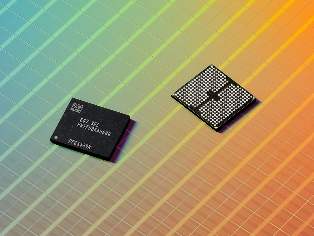
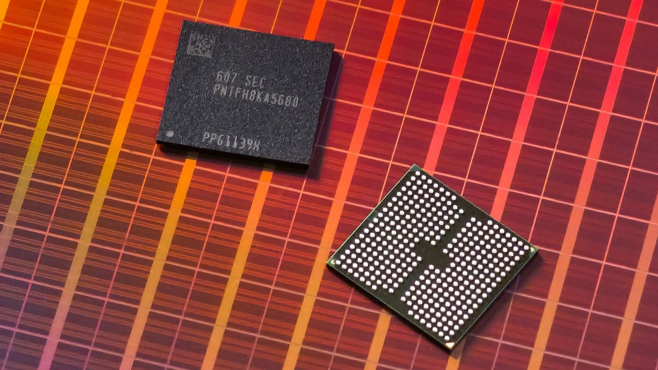
Samsung also unveiled zNAND-O, a high-performance NAND memory currently in development that will enable putting four or eight stacks of NAND devices on top of logic dies. zNAND-O(n) device is based on the company's V-NAND platform (or rather, BV-NAND) and is meant to combine high storage density with improved I/O performance and low latency.
(Image credit: Samsung)
Samsung claims that the tech is suitable for edge AI systems running real-time, data-intensive inference workloads, though, of course, there are many other applications that can benefit from high-performance on-package storage.
(Image credit: Samsung)
Since the technology is in development, Samsung hasn't shared much information about it, even keeping the schematics of how it plans to put zNAND-O layers on top of a logic under wraps. We can speculate that since Samsung mentions 'improved I/O performance and low-latency,' it may be planning to exploit both the inherently parallel architecture of NAND memory with a high-performance interface, though we will not try to dive into details for the sake of not making the discussion too speculative.
BV-NAND: Good old V-NAND gets a new treatment
With BV-NAND, Samsung is essentially introducing a new brand name for its next-generation 3D NAND that bonds the NAND array on top of the I/O and logic wafer. This, in turn, produces the layer itself using high-performance logic process technologies and enables higher I/O speeds.
(Image credit: Samsung)
Samsung formally announced its 400-layer-class V-NAND (aka 10th Generation V-NAND) some time ago, and even disclosed that its areal density would be 28 Gb/mm2 with a maximum I/O speed reaching 5600 MT/s. This likely stipulates the usage of a pinout that is different from the 3D NAND packages used today. While the areal density of Samsung's 10th Gen TLC V-NAND is slightly lower when compared to that of Kioxia/Sandisk's BiCS10 TLC NAND, its maximum I/O speed is significantly higher, which perhaps justifies the new branding.
NAND Layer Counts
Samsung
Samsung
Sandisk/Kioxia
Sandisk/Kioxia
Kioxia/Sandisk
Micron
SK hynix
YMTC
YMTC
Generation
V10
V9
BiCS10
BiCS10
BiCS 8
Gen 9 (G9)
Gen 9
?
Xtacking 3.0/Gen 4
Layers
4xx-Layer
290-Layer (?)
332-Layer
332-Layer
218-Layer
276-Layer
321-Layer
232-Layer
232-Layer
Density
28 Gb mm^2
17 Gb mm^2
>37 Gb/mm^2
>29 Gb/mm^2
22.9 Gb mm^2 (?)
21.0 Gb mm^2
20 mm^2
>20 Gb mm^2
19.8 Gb mm^2
Architecture
TLC
TLC
QLC
TLC
QLC
TLC
TLC
TLC
QLC
Die Capacity
1 Tb
1 Tb
?
1 Tb
2 Tb
1 Tb
1 Tb
1 Tb
1 Tb
I/O Speed
Up to 5600 MT/s
Up to 3200 MT/s
Up to 4800 MT/s
Up to 4800 MT/s
Up to 3600 MT/s
Up to 3600 MT/s
?
?
?
Considering the fact that Samsung rarely sells its memory to third parties and prefers to market client SSDs itself, a new brand for memory can be a sales driver, even if actual high-end drive performance is limited by a PCIe 5.0 x4 interface rather than by 3D NAND memory I/O. Then again, the performance of mid-range PCIe Gen5 SSDs that rely on a quad-channel NAND controller depends on 3D NAND I/O today, so marketing them under a new flash memory brand is a certain way to attract attention and then sell decent performance.
Samsung's new brand strategy
As the new name of the FMS tradeshow implies, the announcements touch upon very distinct industry needs. In the case of Samsung, we are talking about high-performance data center-grade AI accelerators; applications that need storage with latency that is lower than ~50 – 60 µs of modern high-end PCIe SSDs, though we will see how it compares to Z-NAND, and essentially a new generation of conventional 3D NAND with a new brand.
Except for the 400-layer-class Samsung BV-NAND that is set to hit the market in the foreseeable future, the company's new tech, like zHBM and zNAND-O, is years away.
Google was among the first hyperscalers to develop its own custom AI processors about a decade ago and has been steadily ramping their deployment since then. The company seems to be so confident about its TPU v9 due in 2028 that it intends to order 12 – 15 million of such processors, according to a Fubon Research note to clients published by Sean. If the information is correct, Google may not only produce more or a comparable number of AI accelerators than Nvidia, but may also need to use Intel Foundry to meet its goals.
"Based on our checks, Google plans to have 12 – 15 million TPUs in 2028," the paper reads. "Entering 2028, Google’s TPUs will enter the V9 generation with four compute dies, suggesting that their capacity consumption will more than double in 2028 versus 2027."
Fubon estimates that Nvidia supplied 8.2 million data center AI GPUs in 2026 and is on track to increase the number to 12.4 million in 2028. If Fubon is correct about Google's plans to produce 12 – 15 million 9th-generation TPUs in 2028, then the company may produce more, or at least a comparable number of AI accelerators, than Nvidia in 2028.
TSMC is not enough
How the performance of Google's v9 TPUs will stack against Nvidia's Rubin and Rubin Ultra is something that remains to be seen, but the fact that Google intends to use four compute chiplets on these AI accelerators clearly points to the fact that the company bets big on the performance of these processors. Meanwhile, building an AI accelerator with four large compute chiplets is a major engineering effort, which Google seems to have accomplished.
"Although we do not have the detailed allocation yet, we think it is difficult to reach Google’s target with TSMC alone, and Intel's supply is a must by 2028," the paper continues.
Researchers from Fubon are not sure whether Google's allocations at TSMC will be enough to meet the company's demand for 12 – 15 million 9th Generation TPUs, so they think that Google will have to use Intel Foundry's capacity to meet its volume goals. Over the past few months, we have seen reports claiming that Intel had landed orders to make three million TPUs for Google following months of Google's testing of Intel's advanced packaging technologies. Indeed, if Google wants to make its silicon at Intel Foundry, usage of Intel's advanced packaging services makes great sense. It should be noted that when compute chiplets are developed, they must be developed with their packaging technology in mind, as Intel's EMIB/EMIB-T and TSMC's CoWoS-L are incompatible.
World's largest consumer of AI accelerators
If the information about Google's plans to produce 12 – 15 million TPUs in 2028 is correct (note that the difference between 12 and 15 is 20%, which is huge) and Google will indeed deploy more AI accelerators annually than Nvidia sells to the entire market, it would mark a dramatic shift in the AI hardware landscape. It will not only make Google the world's largest consumer of AI accelerators (as the company will unlikely cease buying Nvidia hardware), it will eventually make Google the owner of the world's most capable AI hardware fleet. Whether or not Google will use its overwhelming AI compute capacity primarily for its own services, or will lend the majority to other is something that remains to be seen.
Meanwhile, for Google's rivals, the milestone will underscore the growing importance of vertically integrated AI infrastructure, where cloud providers design chips tailored to their own software stacks, workloads, and data centers instead of purchasing off-the-shelf GPUs.
Yet, Google's surpassing Nvidia in unit shipments would not necessarily diminish Nvidia's dominant position. AI demand continues to expand so rapidly that both companies could increase deployments simultaneously, but Google will simply grow faster, at least till Nvidia ups production of its AI accelerators with Feynman and Feynman Ultra in 2029 – 2030. After all, Nvidia's AI GPUs are sold out. What Nvidia should worry about is not the volumes of TPUs that Google can deploy, but rather the fact that these processors do rely on a software stack that rivals Nvidia's CUDA, the company's main competitive advantage.

 Login