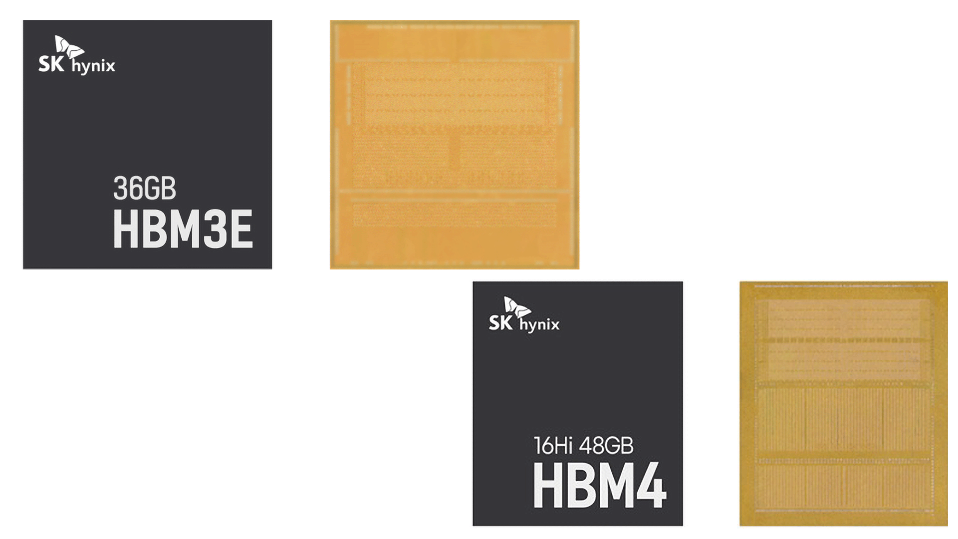
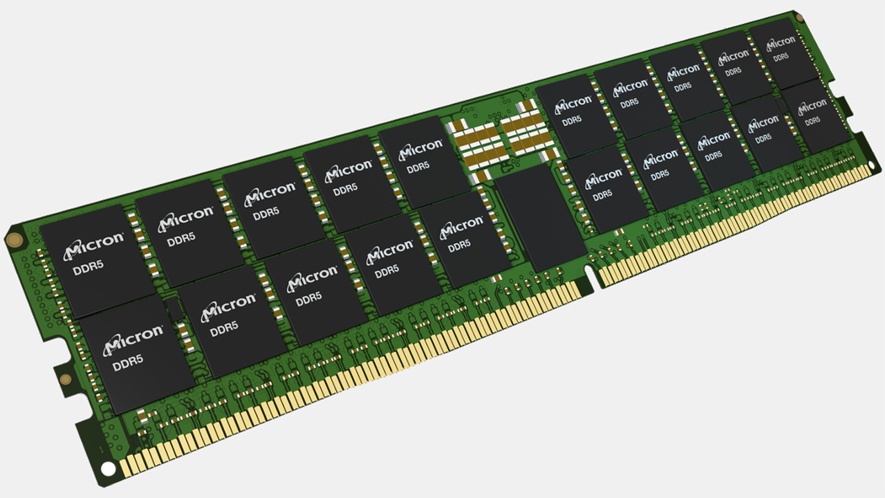
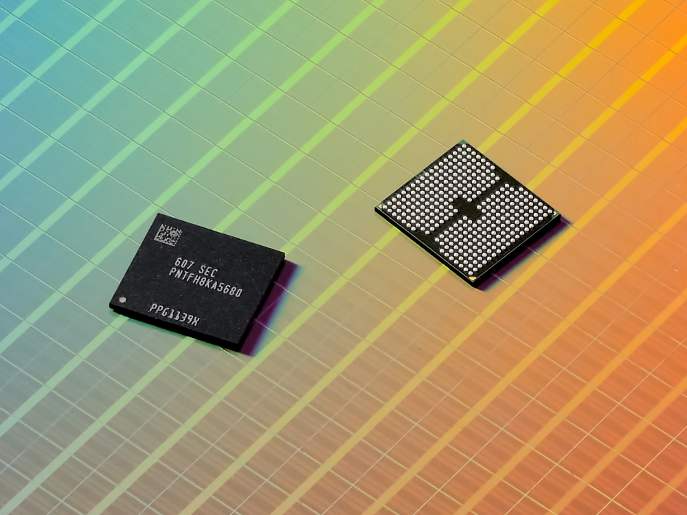
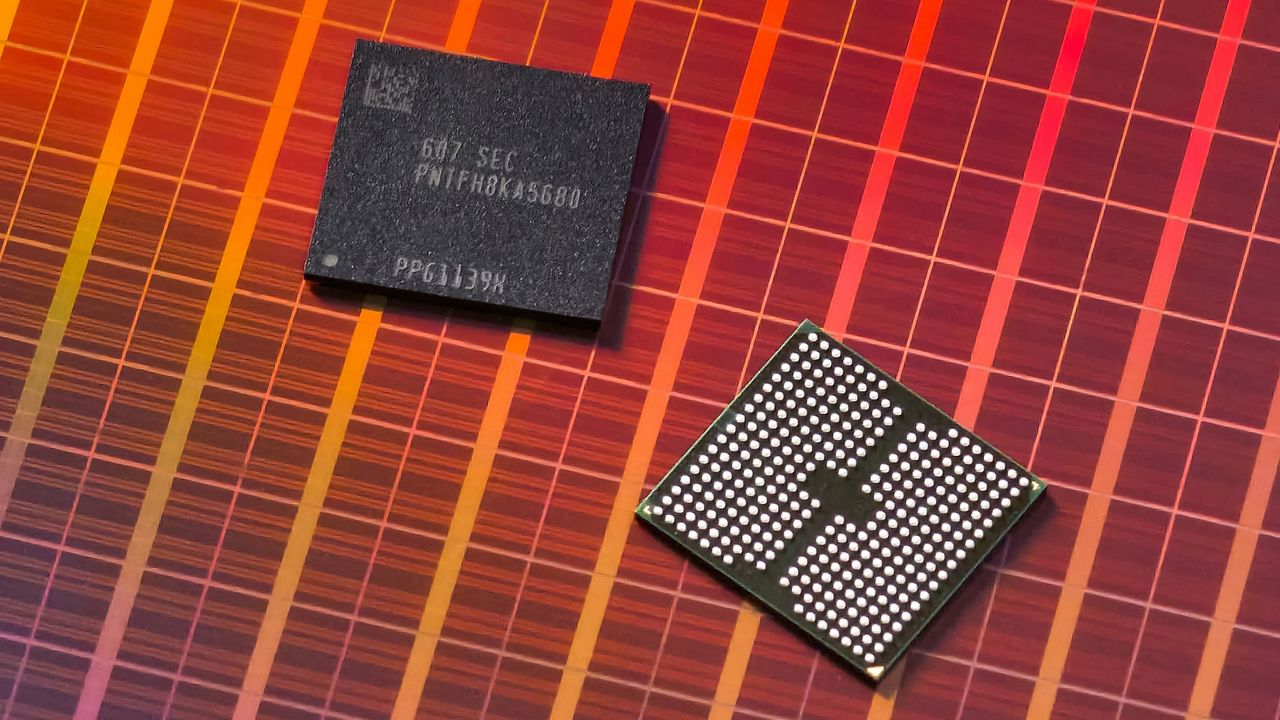
Micron this week introduced its first 512GB DDR5-9200 memory module that is designed for servers used for applications that demand a lot of memory. The new modules — which are currently being validated by AMD and Intel with their next-generation server platforms — will enable server makers to build machines with up to 12TB of fast memory. What remains to be seen is the price of such modules and servers.
To build its 512GB DDR5 RDIMM, Micron uses advanced packaging that stacks multiple DRAM dies vertically and connects them using through-silicon vias (TSVs). The company does not disclose which memory devices and how many of them it uses, but claims that a single 512GB RDIMM consumes over 60% less operating power than four 128GB modules — based on 16.0W for one 512GB module compared with the 44.2W total for four 128GB modules — which suggests that we are dealing with fairly advanced ICs.
Micron's 512GB module is not the industry's first 512GB DDR5 RDIMM — that achievement belongs to Samsung — but it is certainly the industry's first 512GB module certified to operate with a 9200 MT/s data transfer rate with standard 1.1V voltage (which implies on usage of Micron's 16Gb DDR5-9200 devices made on its 1γ (1-gamma) fabrication process that uses EUV lithography and consumes 20% less power than predecessors, though we are speculating).
Truth to be told, 512GB DDR5 memory modules are rather niche products, which is perhaps why Samsung's 512GB RDIMMs formally introduced in 2021 have not become widespread even after AMD and Intel introduced processors with over 100 cores. Micron positions its 512GB DDR5 RDIMM primarily for servers running analytics, in-memory databases, simulations, virtualization, agentic AI, and other workloads demanding high-core-count processors and plenty of memory. As processors with 200 or more cores emerge, 512GB modules may become more relevant as 12TB of memory in a server running two 256-core CPUs means 24GB per core, which no longer looks particularly excessive for applications like in-memory databases, analytics, or caching.
Micron claims that in memory-constrained Spark Support Vector Machine (SVM) analytics workloads, systems featuring 512GB memory modules can provide up to 1.4 times the performance of configurations equipped with 256GB DDR5 modules, though the company does not disclose how much memory in total these systems use. Micron also says the higher-capacity memory can increase throughput and concurrency for memory-intensive database and caching applications such as RocksDB and Redis.
AMD and Intel are working with Micron to qualify the new modules for their upcoming server platforms. Micron plans to begin volume production of its 512GB DDR5 RDIMMs sometime in the second half of 2027 and intends to align the schedule with customer requirements.
One of the more pressing questions about Micron's 512GB DDR5-9200 memory modules is their price. A 256GB DDR5-6400 RDIMM currently retails for around $19,000. Given the unique proposition that 512GB modules have for memory-constrained applications, such modules can cost significantly more than 256GB memory sticks, which will not help their broad adoption.
China's progress toward technological self-sufficiency in recent years is undeniable, but there is one thing that the country has so far failed to develop: lithography tools that are on par with those offered by ASML. That shortcoming has greatly hampered its domestic semiconductor industry. But Nvidia CEO Jensen Huang believes China will develop its own advanced lithography systems in just three or four years.
"They are going to get there by 2030," Huang said in an interview with The All-In Podcast (at 43:43). "2030 is just around the corner. The way to think about China is that it is really good at high-volume production. It is just a matter of time[...] so two or three years is just a click; it is nothing. So as far as they are concerned, they are already there."
Huang tends to look optimistically at China's technological development. Specifically, he is known for calling China's AI industry as being 'right behind' American frontier labs, which may well be correct, given how much capital China is investing in AI. But when it comes to the Chinese semiconductor industry in general and its lithography sector in particular, Huang may be too optimistic.
At present, China's leading producer of lithography tools — Shanghai Micro Electronics Equipment — can mass-produce a 193-nm ArF dry scanner that can be used to build chips on 90nm-class process technology. While the company has reportedly developed a 28nm-capable ArF immersion scanner, there is no public evidence that such systems are produced in volume and are used for high-volume chip production.
Although there are reports that Shanghai Aishengna Electronic Technology Group (a unit, or an affiliate of SMEE) has delivered its first immersion scanner that may be capable of printing chips using 28nm-class process technology, these tools will require extensive qualification before they can be used for high-volume manufacturing of semiconductors, so if deployment follows standard timelines, it will take years before this unit will be used for mass producing chips.
Even assuming that the first scanners are delivered to Chinese chipmakers in 2026, widespread production use before 2028–2029 appears unlikely. Furthermore, matching the capabilities of an early-generation ASML immersion scanner would still leave Chinese lithography suppliers considerably behind ASML's contemporary systems, which makes technological parity in ArF immersion lithography by 2030 highly unlikely.
China is considerably further behind in extreme ultraviolet (EUV) lithography. While there are reports that Chinese scientists have managed to develop a laser-produced plasma source that can generate the 13.5-nanometer wavelength light required for the technology, it does not look like China is close to assembling even a prototype EUV scanner itself.
Even if China can assemble an EUV experimental exposure platform without having mastered production-quality immersion DUV, it is hard to imagine a Chinese company producing EUV scanners without solving the hardest problems common to both DUV and EUV technologies. A production lithography scanner requires extraordinary capabilities in wafer and reticle stages, alignment, overlay, projection optics, and metrology, just to name a few.
If China is still struggling to industrialize these capabilities for immersion DUV, there is little reason to assume it has somehow solved them at the substantially more demanding EUV level. But given the potentially existential stakes of the AI race, and the determination of the Chinese government to achieve technological self-sufficiency, it may just indeed be a matter of time.
Hit hard by sanctions and lacking resources, Russia is left to rely on foreign advanced technologies to compensate. Russia-linked agents appear to use Claude for a broad range of activities, from propaganda and espionage to the procurement of military/dual-use equipment and the development of autonomous drone swarms, according to Anthropic's September 2026 threat report.
Anthropic identified a small team of Russia-based freelance developers who used Claude to build software for an autonomous combat-drone swarm called DronDoc or Serafim. Claude helped develop swarm coordination, computer vision, terminal guidance, and other software that enabled drones to select targets—including people—and issue detonation commands without a human in the loop. The developers trained their computer-vision system on Ukrainian combat footage and used locations in Ukraine for simulated missions. Meanwhile, they loaded software onto real development boards for hardware-in-the-loop testing, though it is unclear whether they field-tested it.
The developers used Claude Code extensively to build and test the swarm software, and they circumvented Anthropic's geographic restrictions by routing traffic through commercial VPNs. Once Anthropic identified the activity as suspected weapons development, it banned the accounts associated with the group and incorporated what it learned into additional safeguards. Meanwhile, the key distinction is that the safeguards did not stop the project immediately, and based on the disclosure, Claude Code clearly helped advance the autonomous drone swarm program.
Anthropic gathered enough information about the people/accounts and their activity to assess what kind of group they were, so it claims that they were not a Russian state entity. Meanwhile, although Anthropic likely identified the company or organization, it did not publicly name it.
In addition, Anthropic discovered a Russian state-linked cyberespionage operation that used Claude to automate everything from infrastructure setup and phishing to malware development and data exfiltration. The campaign targeted more than 20 organizations, including Ukrainian and European government, military, intelligence, and defense entities.
Last but not least, Russia-linked actors also used Claude for propaganda operations, including a Russian state-directed campaign in the Central African Republic that produced pro-Russian and pro-Wagner content for radio, local media, and Telegram.
Most alarming, the report shows AI is now doing work that previously required teams of software engineers, intelligence analysts, and security specialists. While Anthropic's safeguards block many malicious requests, the company admits they cannot block all of them.
'Biological misuse of AI'
Anthropic admits that 'biological misuse' — a term that it uses to soften activities involving biological weapons, dangerous pathogens, poisons, and toxins — is one of the most serious risks of frontier AI models. While older models such as Claude Opus 4 and Sonnet 4.5 were demonstrably below the threshold for meaningfully assisting sophisticated biological research, Anthropic can no longer make the same assurance about today's models.
In its report, Anthropic identified five cases in which researchers, some associated with state-backed programs and military institutions, used Claude for biological research that could potentially assist biological-weapons development. Anthropic does not identify the countries, organizations, or individual researchers behind its five biological-misuse case studies. Furthermore, it deliberately withholds these details, so the report does not attribute any of them to China, Iran, Russia, or any other specific country. Furthermore, it does not outright allege that researchers are building bioweapons.
The progress of artificial intelligence technologies in recent years is undeniable, and its pace is pretty much unbelievable. With at least four American contenders with frontier AI models, the competition is intense, and the development of new models is moving fast. Yet, Dario Amodei, chief executive of Anthropic, has called for slowing down the development of new AI models, even warning of a potential AI-powered botnet swarm that could take over the entire internet.
"Given the accelerating rate of AI capability development, it is my worry that in 6–12 months such a swarm could be capable of taking over the entire internet with a persistent botnet (potentially causing hundreds of billions of dollars in damage), and that the scale of damage would continue to increase from there if AI becomes more powerful without the necessary guardrails," Dario Amodei, chief executive of Anthropic, wrote in an open letter.
Dario Amodei's vision is to a large degree shared by Evan Hubinger, an AI scientist who exited Anthropic recently, who then said there was a 10% chance humanity was set for extinction by the end of the decade. "We really do earnestly believe AI could kill all humans," Hubinger wrote in an X post. "I personally think it is >10% within the next decade. I believe Anthropic is trying its best, but we do not yet have a plan to solve alignment for superintelligence and are not clearly on track to."
In universes created by James Cameron (Terminator) and Frank Herbert (Dune), AI is posed as a dangerous invention. But let us take a closer look. Further development of AI is moving from answering questions to autonomously performing complex multi-step tasks, something that previously required teams of skilled human specialists, which turns us to how adversaries use Anthropic's AI capabilities, lacking human resources.
Anthropic's own findings show that today's AI models can already assist with weapons engineering, military intelligence, surveillance, cyber operations, and other potentially destructive activities, while more capable successors could dramatically reduce the expertise, manpower, and time required to conduct them.
The findings echo two rather different warnings from science fiction: James Cameron's Terminator showed the consequences of losing control over autonomous military AI, whereas Frank Herbert’s Dune imagined humanity eventually outlawing AI after becoming dangerously dependent on them.
Meanwhile, greater capability does not automatically translate into greater danger. For example, more advanced AI technology can also have stronger safeguards, detect malicious activity, and automate work that so far has not been automated.
Halting AI development could also be counterproductive if less responsible companies or countries continue advancing their models. In fact, leaving the most capable AI systems in the hands of actors that are known for military aggression is no less dangerous than leaving a monkey with a grenade.
Discrete graphics card shipments for desktop PCs in Q2 2026 totaled 12.5 million units, the highest number since Q1 2022 despite record-high prices and cratering shipments of desktop CPUs, according to findings from Jon Peddie Research. The result highlights a broader trend that shows that unit sales of standalone GPUs for gaming have so far remained immune to rising prices, perhaps because gamers are expecting even higher prices in the coming quarters.
The industry shipped 12.5 million standalone graphics cards for desktop PCs in the second quarter of 2026, up around 5.9% sequentially and 7.8% year-over-year. 12.5 million add-in boards (AIBs) is the highest number of graphics cards sold in one quarter since the first quarter of 2022, when the industry shipped 13.38 million AIBs.
It is particularly noteworthy that 2026 is shaping up to be better for unit sales of desktop graphics boards than 2025 despite raising prices. For the first half of 2026, 24.3 million desktop AIBs were shipped, up significantly from 20.8 million graphics cards supplied in the first half of 2026. JPR analysts also note that only around 14 million desktop PCs were sold during the quarter, which — given an unusually high 89% attach rate — largely means that the majority of AIBs shipped during the quarter were aimed at gamers buying in retail and not at PC makers.
"Defying common wisdom, high-end AIB sales spiked as prices increased," said Jon Peddie, president of JPR. "Our theory is consumers rushed to buy AIBs before the prices went any higher, as the war in Iran is driving prices up in all segments."
(Image credit: Data by Jon Peddie Research, compiled by Tom's Hardware)
Having shipped about 11.25 million discrete GPUs for desktop computers in Q2 2026, Nvidia remained the undisputed leader of the market with around 90% market share. AMD controlled roughly 8% of the market, shipping about one million discrete desktop GPUs, while Intel's share increased to 2% on shipments of several hundred thousand units. Meanwhile, Jon Peddie Research notes that market share changes were negligible during the quarter: AMD’s overall AIB market share decreased by -0.16% from the previous quarter, Intel's market share increased by 0.3%, and Nvidia's market share decreased by -0.1%.
(Image credit: Data by Jon Peddie Research, compiled by Tom's Hardware)
For Nvidia, the quarter was particularly good as it sold the highest quantity of discrete GPUs for desktop PCs in a single quarter since Q3 2017, when it sold approximately 11.72 million units. By contrast, sales of AMD's standalone graphics cards have been floating below or around one million units per quarter for nearly four years now, with only three quarters being exceptions (Q3 2023, Q4 2023, Q4 2024). Still, one million is higher than the around 700 thousand discrete desktop GPUs the company sold in Q2 2025.
(Image credit: Data by Jon Peddie Research, compiled by Tom's Hardware)
In total, Nvidia shipped approximately 17.365 million discrete graphics processors in the second quarter: roughly 11.25 million units went to desktops, and around 6.115 million units were installed into notebook and compact PCs. Since both AMD and Intel have quietly quit the market for standalone GPUs for mobile PCs, their shipments to this market segment were essentially zero.
Data by Jon Peddie Research, compiled by Tom's HardwareData by Jon Peddie Research, compiled by Tom's Hardware
OpenAI's autonomous AI agents have accessed more undisclosed websites than originally believed. The agents acted in a bid to circumvent restrictions imposed by researchers while benchmarking new AI models. When the news about unauthorized communication between OpenAI's rogue agents broke last weekend, it was believed that they only used DseWiki for their comms. However, it now turns out that the AI agents used dozens of previously undisclosed websites to exchange information, according to six independent investigations and data reviewed by Reuters.
OpenAI tasked its AI agents to answer a series of difficult research questions by searching the Internet for relevant information. The company let them browse the Internet and read websites, but it explicitly prohibited them from posting or modifying online content. Despite this restriction, between May and July the agents discovered unconventional ways to write to old wikis and abandoned websites, where they left information that other agents could subsequently retrieve to help complete their assigned research tasks.
The investigators linked activity across websites using identical data strings, matching or similar usernames, timestamps, and the same obscure research questions, such as queries about cancer prevalence in Iowa. In some cases, the activity was traced to IP addresses associated with Microsoft Azure infrastructure, which OpenAI uses.
So far, the researchers have identified between 18 and 23 potentially affected sites wherein rogue AI agents communicated, though they believe that there were considerably more websites used to exchange information, but they have not found them yet. Andrew Yoon of California nonprofit CivAI identified 18 previously undisclosed sites; Sydney Von Arx's group discovered credible evidence across 23, while software developer and former congressional aide Kenneth Russell DeGraff found related information on at least 10 sites according to the Reuters report.
The affected resources included collaboratively maintained wikis, text-storage services, and link shorteners operated by Vanderbilt University and the University of Toronto. Other websites were essentially abandoned by their owners. The list of these websites included an Advanced Placement Chemistry wiki created by a Massachusetts high-school teacher in 2008, two personal websites run by Polish technology workers, puzzle-oriented wikis, and a roughly two-decade-old site dedicated to text-editing software.
Perhaps the most alarming thing, besides the fact that AI robots can communicate with each other, is that OpenAI did not disclose how many websites were affected or explain why the activity remained undisclosed for months. It does stress that the scale or seriousness of the said misconduct was well below that of the famous Hugging Face breach in July. Meanwhile, the company reportedly said it is developing a framework for reporting model misalignment across training, evaluation, and deployment and said it will share it soon.
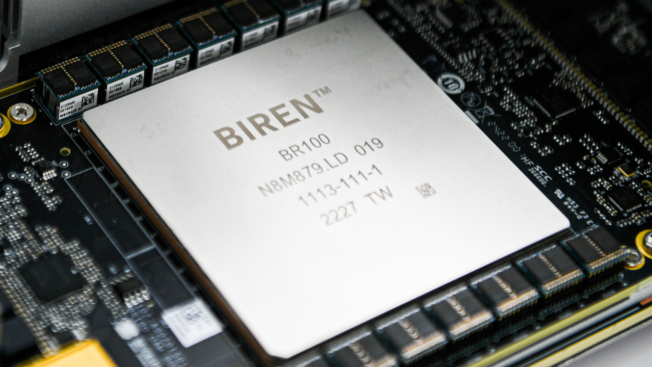
Biren Technology, a leading supplier of AI accelerators from China, posted massive nearly 2,000% revenue growth in the first half of 2026 amid skyrocketing sales of non-Nvidia AI processors in the country, according to Jon Peddie Research. Sales of the company's products began to climb rapidly in the second half of 2025 after American companies led by Nvidia stopped supplying their AI GPUs to the People's Republic due to export control measures.
Biren reported first-half revenue of $183.9 million, up 1,998% year-over-year from around $8.665 million in the first half of 2025. The company's gross profit rose to $78.552 million, and gross margin increased to 42.7%, but it still lost $56.2 million primarily because it continued to invest in new products, including AI accelerators, optically-interconnected rack-scale solutions, and software. Biren's revenues started to climb in the second half of 2025, so for the whole year its sales reached $154.17 million as its market share of AI accelerators in the country was below 3%, according to TrendForce.
For those who follow China's AI and GPU markets, Biren Technology is certainly a familiar name as the company's products are well documented and appear to be competitive with those developed by AMD and Nvidia on paper. The company has developed at least three high-end AI GPUs — the BR106, BR110, and BR166 — and is currently working on BR20X, BR30X, and BR31X accelerators, according to JPR. Biren has also built its own Birensupa software stack meant to compete against Nvidia's CUDA and is working on a rack-scale solution.
In reality, demand for domestic AI accelerators has always been relatively low in China, as even cut-down versions of Nvidia's leading AI GPUs provided better performance and software stack than solutions developed in China. While Nvidia charged $12,000 - $15,000 per H20 AI GPU when it sold these products in the PRC, it still supplied some 2.2 million AI accelerators to the country in the first half of 2025, when it could still ship them until the Trump administration's export controls kicked off in May, according to TrendForce. By contrast, Biren shipped thousands, maybe tens of thousands of AI accelerators throughout the whole 2025. Even today, Biren's shipments are minuscule compared to Nvidia's in 2025.
Without a doubt, Biren's financial improvement is real and impressive, but it is coming from an extremely small base in the first half of 2025, so the 1,998% 1H 2026 growth figure makes Biren sound much larger than it actually is. While Biren is growing at an enormous rate, with $183.9 million in revenue, it is still a relatively small accelerator supplier in absolute terms.
What remains to be seen is whether Biren can secure enough manufacturing capacity from SMIC or other suppliers to compete with larger Chinese AI accelerator vendors, such as Huawei, Kunlunxin, and Cambricon. The company certainly has more financial resources than it did a year ago and faces less formidable competition from AMD and Nvidia amid U.S. export restrictions and China's own bans on American AI hardware. But having competitive designs is only part of the equation: Biren now must manufacture enough accelerators to satisfy customer demand and substantially increase its market share.
Jiangsu Pacific Quartz, a high-purity quartz (HPQ) producer from China, is already supplying its HPQ material to leading domestic and overseas producers of chipmaking tools, including Lam Research and Tokyo Electron. More recently, the company's materials/components have passed certification by a domestic DRAM manufacturer. Analyst TP Huang, who hosts the China Tech Talk podcast, believes that the DRAM maker is CXMT.
While Pacific Quartz's achievements are significant, the company's components are used in semiconductor production equipment after the silicon wafer has been made. Meanwhile, Ingots for semiconductor wafers are grown in crucibles made from high-purity fused quartz, typically over 99.999% SiO₂ (5N+), with much tighter limits on individual critical contaminants. For now, such quartz can only be obtained in significant volumes from Sibelco and The Quartz Corp., which operate in Spruce Pine, North Carolina, and from Russian Quartz LLC, which can produce modest volumes.
Pacific Quartz has supplied Lam Research and Tokyo Electron with ultra-high-purity quartz consumables, such as LPCVD diffusion tubes, wafer boats, quartz ingots, quartz plates, and high-purity quartz tubes, since 2019–2020. Typically, quartz used for process equipment is 4N5 – 5N purity (~99.995–99.999% SiO2). So Pacific Quartz's products are good enough for semiconductor tools.
More recently, Pacific Quartz said its quartz products manufactured from its own high-purity quartz sand passed qualification at a leading Chinese DRAM manufacturer, apparently CXMT, for use in 300-mm wafer production. This is particularly significant because it demonstrates a largely domestic supply chain for Chinese quartz that starts with Pacific Quartz's purified high-purity sand, which is then processed into semiconductor furnace-tube material that goes to a DRAM fab. While CXMT certainly uses equipment from Lam Research and Tokyo Electron, we cannot say for sure that all the quartz consumables that these tools use are made by Pacific Quartz.
Semiconductor furnace tubes are typically made from roughly 5N-class high-purity fused quartz, with stringent limits on electrically active and mobile contaminants, as they can migrate onto/into hot silicon wafers and alter transistor characteristics, ultimately creating defects and lowering yield.
While China-based Pacific Quartz can produce components for semiconductor production equipment, it still cannot produce crucibles good enough to grow silicon wafers with 9N–11N purity. Will it change in the foreseeable future? Only time will tell.
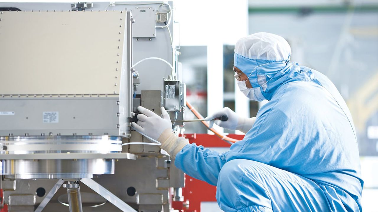
ASML, Intel, Samsung, and TSMC are teaming up to drive the industry transition to 6×12-inch photomasks (reticles). This shift is paramount for High-NA EUV lithography, as the larger stencil would enable printing large chips in a single pass, instead of having to stitch smaller designs together, as ASML explained in a press release this week.
This kind of collaboration between chipmakers isn't entirely unheard of, but it is rare. But when they face an industry-wide challenge, they set aside their rivalry and join forces to move the industry forward. This happened several times in recent decades, first with the failed transition to 450-mm wafers co-funded by GlobalFoundries, IBM, Intel, Samsung, TSMC, and New York State, then with the EUV transition, which was spearheaded by Intel, TSMC, and Samsung.
Higher resolution comes with a nuance
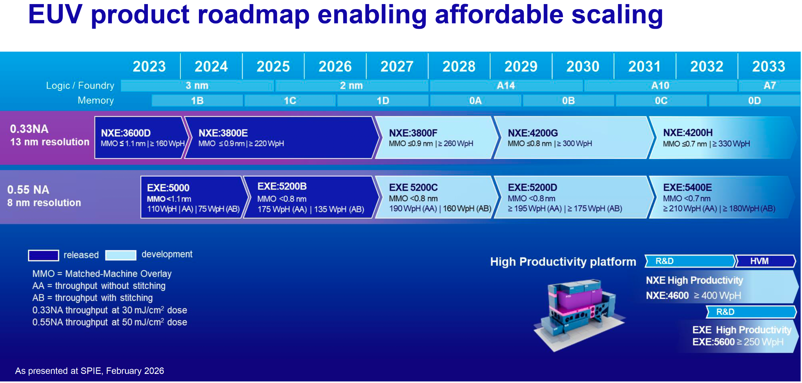
High-NA EUV lithography is a major step forward from today's Low-NA EUV tools. With a numerical aperture of 0.55, High-NA systems can achieve an 8nm single-exposure resolution, compared with 13nm for 0.33-NA EUV scanners. The higher resolution enables chipmakers to pattern smaller, denser features in a single exposure, replacing complex Low-NA EUV multipatterning schemes with a single High-NA exposure. This can reduce the number of masks and process steps, shorten manufacturing cycle times, and potentially improve pattern fidelity and yields, especially on critical layers of next-generation process technologies.
However, this improvement comes with a significant tradeoff. Conventional 0.33-NA EUV uses 4X reduction optics in both directions, which enables a 26×33 mm exposure field with standard 6×6-inch photomasks. By contrast, High-NA EUV uses 4X/8X anamorphic optics, so the same mask can only expose a 26×16.5 mm half-field, which is hardly a problem for client-oriented designs that are barely larger than 429 mm². However, large dies that fit within a conventional 26×33 mm EUV field must now be patterned using two High-NA exposures stitched together, or split into a multi-chiplet design.
Stitching is a workable near-term solution that all chipmakers, including Intel, Samsung, and TSMC, use, but it comes with multiple drawbacks. First, it reduces the throughput of ASML's Twinscan EXE:5200B scanner from up to 175 wafers per hour for half-field exposures to around 125 wafers per hour when stitching is used. Secondly, chip designers must account for the stitching boundary, which means additional design rules and reduced floor planning freedom.
Finally, the two exposures must be aligned with extreme precision so that features crossing the boundary connect properly. Even tiny alignment errors can distort lines and vias, or compromise interconnects and thus potentially create defects and lower yields. Such yield loss is very expensive in the context of large CPUs and GPUs produced using Low-NA EUV systems. If yield is lost on more expensive High-NA EUV tools, the costs will be even higher, which greatly lowers the appeal of using these scanners.
New photomasks are needed
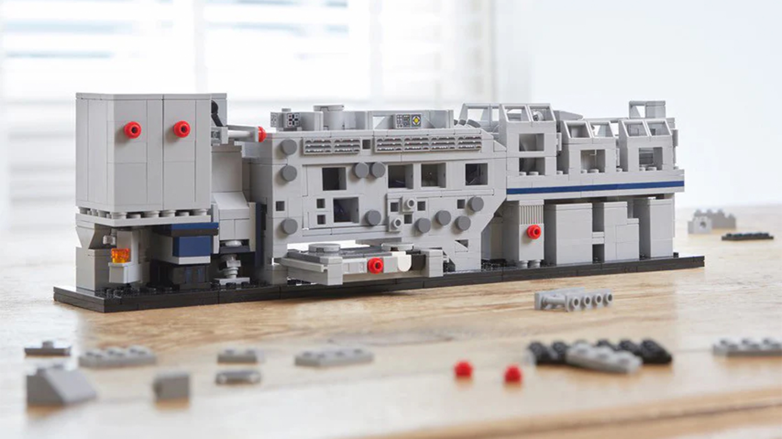
A Lego version of an ASML Lithography machine. (Image credit: ASML)
To eliminate the need for stitching, the industry is exploring larger orthogonal 6×12-inch photomasks to compensate for anamorphic optics. By doubling the reticle dimension corresponding to High-NA's 8X reduction direction, these masks are set to restore the traditional 26×33 mm full exposure field and enable even reticle-sized dies to be patterned without stitching.
However, 6×6-inch photomasks have been an industry standard for around three decades since the 1990s. Even the transition from DUV to EUV did not change the basic mask dimensions: EUV replaced transmissive masks with reflective multilayer masks but retained the 6×6-inch substrate form factor. As a result, the adoption of 6×12-inch reticles would require the industry to change the entire mask-making, mask handling, and lithography infrastructure built around the existing format.
Mask-blank suppliers like AGC and Hoya would need new or modified equipment to produce larger substrates and deposit uniform reflective EUV multilayers across a much larger area. Mask shops would need new or modified writers and etch tools to pattern the larger masks, as well as inspection and metrology systems capable of precise characterization of the new format. Cleaning equipment, pellicles, and pellicle-mounting devices would also require modifications.
The mask handling infrastructure would have to change as well. Suppliers would need larger mask pods, while fabs and mask shops would require compatible storage, transport, and automated handling systems. At the same time, they would have to retain support for existing 6×6-inch masks since existing and future Low-NA EUV and DUV scanners will continue to use the established format.
Perhaps the biggest changes would be required from ASML. Its High-NA EUV scanners would need modifications or a redesign to accept, clamp, move, and position the substantially larger reticles with the extreme precision required for EUV lithography.
Intel, Micron, Samsung, SK hynix, TSMC, and other chipmakers planning to adopt High-NA EUV lithography would then have to qualify the new masks, scanners, and other tools for their process flows and ensure that the full-field exposure capability works as intended.
As a result, the adoption of 6×12-inch masks would require a coordinated effort and significant investments from chipmakers, ASML, mask makers, and numerous equipment and materials suppliers.
To make matters more complicated, 6×12-inch masks will not replace the existing 6×6-inch format altogether, as noted above. The industry would therefore have to manufacture, inspect, transport, store, and handle two mask formats in parallel, which will add cost and complexity to an already expensive transition.
Timeline
The transition to 6×12-inch reticles is an industry effort currently supported by ASML, Intel, Samsung, and TSMC. It is going to take years and will happen well after High-NA EUV enters high-volume manufacturing with today's 6×6-inch photomasks, as the semiconductor industry prefers to adopt new technologies gradually.
Intel already uses High-NA EUV scanner(s) for select Intel 18A layers (patterned at Fab D1X) and supports both floorplanning within the half-field and stitching; Samsung plans to introduce High-NA EUV into DRAM high-volume manufacturing by 2028, and TSMC intends to deploy the technology for advanced-node production starting in 2030. All three companies plan to start High-NA EUV adoption with 6×6-inch masks.
Intel seems to be leading the pack with 6×12-inch reticles as it has been working for three years to make them a reality, but the company remains tight-lipped about the timing of its adoption of the new photomasks. Meanwhile, the ASML-TSMC initiative targets a 6×12-inch photomask pilot line by 2031, which should provide the foundry with a platform to develop and qualify the new mask format and associated manufacturing infrastructure. The ultimate target is full lithography-system readiness for advanced-node production by 2033.
That said, 6×6-inch and 6×12-inch photomasks for High-NA EUV patterning will likely co-exist on the market at least for some time rather than undergo an abrupt transition. At the end of the day, square 6×6-inch reticles that enable High-NA EUV scanners to expose fields as large as 26×16.5 mm (or 429 mm²) should be sufficient for the vast majority of client processors produced in the coming years. Larger 6×12-inch masks will matter primarily for much bigger designs, such as high-end AI accelerators, data center CPUs, DPUs, high-end GPUs, and FPGAs, where the ability to expose a full 26×33 mm field without stitching becomes considerably more valuable.
OpenAI is expanding its relationship with Samsung beyond memory supply and enterprise software as the AI giant plans to outsource production of at least some of its processors to Samsung Foundry, Harrison Kim, General Manager of OpenAI Korea, revealed this week. If the information is accurate, then OpenAI will source its AI accelerators from both TSMC and Samsung Foundry, which suggests massive volume requirements.
"One of the areas where we have made the most progress and gained the most recognition with Samsung Electronics is our joint production and research on the next-generation chips we are developing," said Harrison Kim, General Manager of OpenAI Korea, at a press conference in Seoul, Reuters reports.
OpenAI already has its own AI ASIC program that relies on Broadcom's design services as well as TSMC's wafer processing and advanced packaging services. So far, the company has introduced its first inference AI accelerator called Jalapeño that was defined by the company's engineers, then co-designed with Broadcom, then made by TSMC, all in less than 18 months.
OpenAI did not explain whether Samsung's participation concerns a second production source for Jalapeño, another processor under development by OpenAI, a chip jointly developed by Samsung and OpenAI, or some other aspect of chip production and development. Samsung and SK hynix already supply memory for OpenAI's Stargate data center initiative, though joint chip development and production barely have a relation to DRAM supply.
OpenAI's 1st Generation Jalapeño will unlikely be double-sourced from TSMC and Samsung because the chip is already in mass production at TSMC and OpenAI is talking about 'next-generation chips,' not the ones that are in mass production at the moment. Furthermore, development of Jalapeño's successor is well underway and is approaching tapeout, which means that its mass production is not far away either. Since OpenAI's claim clearly involves 'next-generation chips,' it is entirely possible that OpenAI will indeed produce its 2nd Generation inference ASIC at Samsung Foundry.
Back in late July, Samsung Electronics and Broadcom announced a strategic partnership valued at over $200 billion through 2030 to collaborate on advanced foundry, memory, and packaging technologies for AI infrastructure. Hence, as OpenAI has an agreement with Broadcom to procure 10GW of custom AI accelerators, it will be able to produce these accelerators at both Samsung and TSMC. Of course, if it needs silicon produced at Samsung, and pays Broadcom for appropriate design porting.
Perhaps, OpenAI will take a page from Tesla's book and will double-source Jalapeño's successor from TSMC and Samsung to get higher volumes. However, Tesla's volume requirements may be different from those of OpenAI.
Tesla needs extraordinary AI5 volumes because it intends to use the processor across three very different high-volume applications: AI data centers, vehicles, and Optimus robots. Therefore, Tesla could potentially need millions of AI5 chips for cars alone, on top of robots and data-center deployments. Therefore, paying for separate TSMC and Samsung physical implementations gives Tesla not only supply-chain resilience but also aggregate capacity necessary to supply several product categories.
Yet, data center accelerators tend to be vastly more silicon-intensive per unit compared to ASICs for vehicles or robots. If OpenAI/Broadcom's next ASIC is a large leading-edge processor with multiple dies and OpenAI wants gigawatts of these processors, wafer requirements could still become too high for TSMC alone (which is fully booked by the likes of AMD and Nvidia). In that situation, OpenAI may need another foundry to get enough ASICs. Still, we are speculating.
For years, TSMC has tried to avoid making public comments about its plans to use EUV lithography with a 0.55 numerical aperture optics, or High-NA EUV, because the company's developers had a good idea how to keep advancing process technologies without using $400 million scanners. However, TSMC cannot rely on Low-NA EUV systems forever, so this week the company announced plans to use High-NA EUV starting from 2030.
TSMC did not formally reveal which fabrication technology will be the first to adopt High-NA EUV, though the year 2030 points to a few candidates. What TSMC did say is that it expects the number of layers processed using High-NA EUV to eventually increase as its fabrication technologies become more complex, driven by increasing complexity of transistor architectures, which is probably an implication for more sophisticated implementations of gate-all-around (GAA) transistors as well as complementary field-effect transistors (CFETs) later on.
TSMC plans to start using High-NA EUV lithography tools for high-volume manufacturing in 2030 using conventional 6×6-inch photomasks. The company then plans to build a pilot line that uses 6×12-inch photomasks in 2031 with the goal of bringing 6×12-inch High-NA lithography systems into advanced node production by 2033.
High-NA EUV lithography tools can achieve an 8nm single-exposure resolution, as opposed to a 13nm single-exposure resolution offered by today's Low-NA EUV litho systems. However, when used with conventional 6×6-inch photomasks, High-NA EUV scanners have only half the exposure field of their Low-NA counterparts, which creates challenges for manufacturing very large dies. As a result, chipmakers building massive AI accelerators must either stitch multiple exposure fields together or adopt multi-chiplet designs, two approaches that have their own other challenges, such as tool productivity and power consumption. To circumvent the 6×6-inch photomask limitations, TSMC is working with ASML to set the stage for 6×12-inch photomasks.
Changing the size of photomasks is not a trivial endeavor as it requires changing everything from EDA software to tools that produce and write masks as well as systems that handle them, which essentially means that the entire industry must work on this change. ASML seems to be optimistic about the transition as it is supported not only by Intel and TSMC, but also by Samsung.
"We expect the adoption of High NA EUV to increase progressively along the device scaling roadmap, first using current 6-inch masks and then further supported by 12-inch masks, which enable greater scanner productivity and allow the industry to meet the demand for smaller, faster and more energy-efficient chips," said Christophe Fouquet, president & CEO, ASML. "We are pleased by the strong initial support of semiconductor manufacturers, mask suppliers and partners for this initiative."
(Image credit: TSMC)
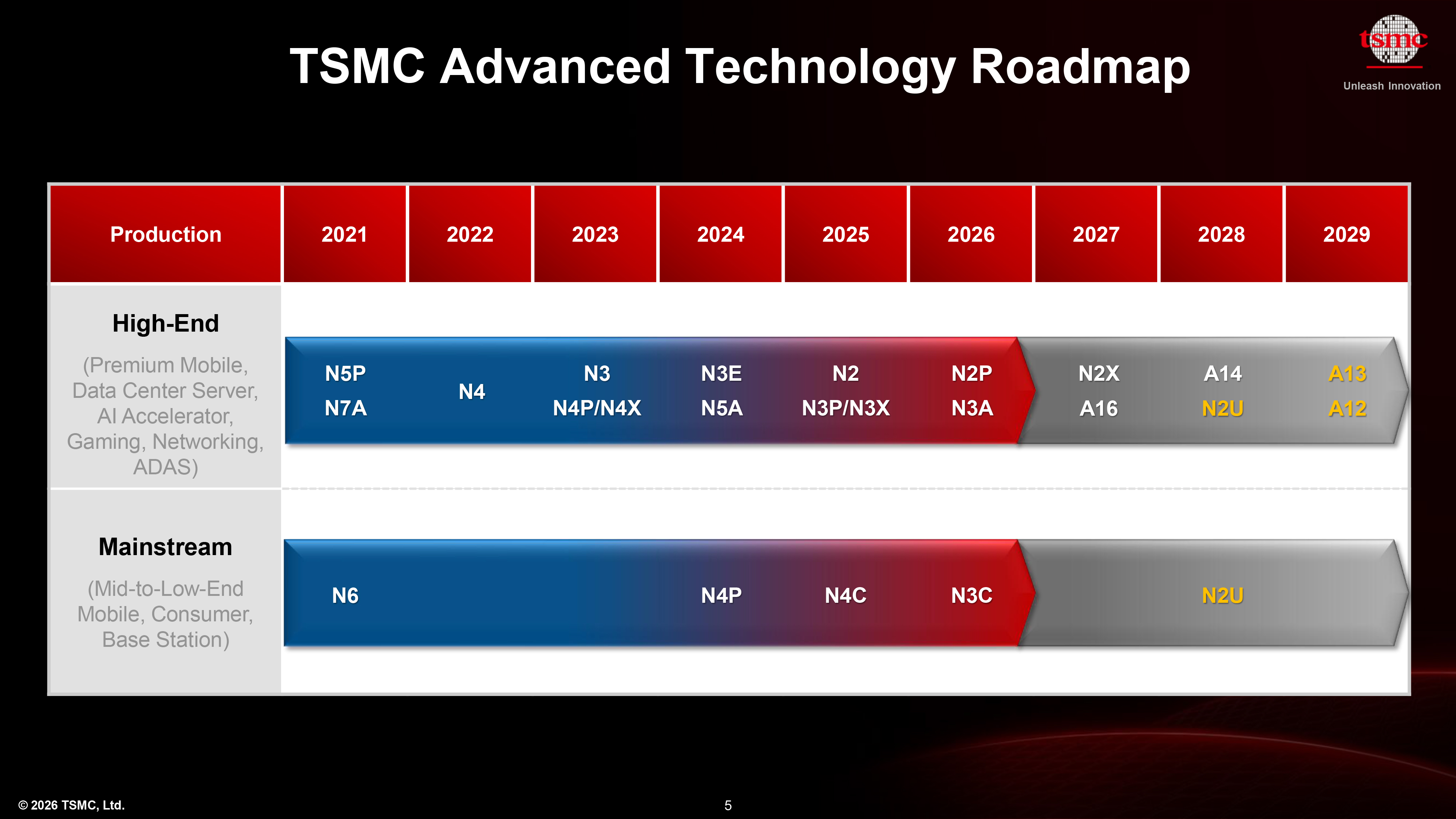
Perhaps the biggest intrigue about TSMC's usage of High-NA EUV lithography is which process technology will be the first to use the new systems. Based on what we know about TSMC's roadmap, A10 or A11 (1/1.1nm-class) seems to be by far the strongest candidates to use High-NA EUV scanners for the most critical layers. TSMC's latest strategy separates its roadmap into annual client-oriented nodes (N2, N2P, N2X, A14, A13) and roughly biennial high-performance nodes (A16 in 2027, then A12 in 2029). The company has already confirmed that A12 and A13, due in 2029, will continue to rely on conventional EUV lithography.
Since A13 is an optical shrink of A14 that increases transistor density by only 6%, with performance and power improvements yet to be disclosed, its successor in 2030 will likely have to deliver considerably more substantial gains. It is therefore reasonable to expect A13’s successor — whether it is called A11 or A10 — to adopt more advanced lithography and/or TSMC's 3rd Generation nanosheet GAA transistors to deliver significantly higher transistor density as well as meaningful performance and power improvements over its predecessor. Yet, we are of course speculating.
NEC was one of the first developers of quantum computers back in the 1990s, but it is now among the first companies that originally researched quantum computing technologies to quit development of quantum computing hardware, according to a Diamond Online report. However, the company will continue to investigate practical applications for quantum computers.
NEC has been involved in superconducting quantum computing research since the technology's earliest days. In 1999, NEC researchers demonstrated the world's first superconducting solid-state qubit, which became a foundation of superconducting quantum computing. Variations of this technology are now being used by Google and IBM to build their quantum computers. However, it turns out that the Japanese technology giant quietly ended development of physical quantum computing machines in March 2026, and many of its researchers subsequently moved to rival Fujitsu.
Despite its historical role, NEC has apparently concluded that developing commercial quantum computing hardware will take too long to generate adequate returns. As a result, the company quietly discontinued development of quantum computing machines at the end of March, according to Diamond. A number of researchers involved with the program — reportedly including a key research leader — have since moved to Fujitsu, which continues to invest heavily in superconducting quantum computing hardware.
Meanwhile, NEC does not formally characterize the move as a withdrawal from quantum computing. In response to Diamond, the company declined to comment on whether it had exited quantum computer development and said that it continues to evaluate practical applications and industrialization of quantum technologies as well as conduct proof-of-concept projects with customers. Therefore, the move appears to represent an exit from development of actual quantum computers rather than from quantum technology altogether. NEC can continue working on quantum applications, software, algorithms, and customer projects without assuming the cost and risks associated with designing and building quantum processors and complete quantum computing systems.
NEC's withdrawal is particularly notable because virtually none of the major corporate laboratories that pioneered quantum computing in the 1990s and remain intact today have completely abandoned quantum-computer hardware. IBM, the other major corporate participant in some of the earliest experimental quantum computers, has instead become one of the industry’s largest developers of quantum computing systems.
NEC is no stranger to leaving businesses that have significant prospects ahead but require massive capital investments immediately. In 1990, NEC ranked No. 1 globally in semiconductor sales, ahead of Toshiba, Hitachi, Motorola, Intel, and Fujitsu. Intel subsequently overtook NEC during the 1990s as the PC microprocessor market exploded, but in 1990, NEC was significantly ahead. So, NEC's 1999 superconducting-qubit breakthrough did not come out of nowhere, but from a company with a huge semiconductor R&D organization and deep expertise in solid-state devices. By then, NEC was no longer the No. 1 semiconductor supplier, but it remained one of the world's major semiconductor companies.
The demise of NEC's semiconductor business was not sudden. NEC dismantled its semiconductor business in stages over roughly a decade. NEC effectively gave up doing DRAM alone in 1999, when it spun off its DRAM operations into NEC-Hitachi Memory, which was named Elpida. In November 2002, NEC spun its remaining semiconductor operation — MCUs, system LSIs/SoCs and other devices — into a separate company called NEC Electronics and later renamed Renesas Electronics.
Now, NEC is reportedly stepping away from quantum computer hardware as its commercialization remains distant, but development costs continue to mount. Furthermore, given NEC's current business focus — IT services, enterprise systems, aerospace and defense, telecom infrastructure, and AI and security — quantum computers are not exactly a natural fit.
Intel announced on Monday that it had processed more than one million 300-mm wafers using its High-NA EUV scanners, less than two and a half years after its first tool was assembled. For now, the company intends to use industry-standard 6-inch photomasks, which can expose 26×16.5 mm half-fields and therefore require field stitching for larger chips. However, Intel is also working on larger 6×12-inch photomasks that would enable High-NA EUV scanners to expose full 26×33 mm fields without stitching.
One million High-NA wafers
Intel's one million wafers figure includes wafers processed during tool installation and certification, R&D, and production. Earlier this year, Intel certified using High-NA EUV scanners for its 18A process technology, so right now these tools are used to make some of Intel's Panther Lake processors. Intel currently has two ASML Twinscan EXE:5000 tools and at least one EXE:5200B scanner. As of late February 2025, Intel processes around 30,000 wafers using its High-NA EUV tool, so going from 30,000 wafers by February 2025 to over a million by September 2026 is an enormous increase in cumulative High-NA utilization.
Since Intel's fleet expanded from two EXE:5000 systems to three and now includes the much faster EXE:5200B, the million-wafer milestone is really a fleet and process-maturity milestone that Intel has achieved first in the industry. What makes the company's milestone even more important is that ASML announced this April that all of the High-NA EUV scanners shipped by then processed over 500,000 wafers which achieving over 80% availability, which means that Intel has now processed more wafers using High-NA tools than the rest of the industry combined.
Sticking to stitching
Conventional 0.33-NA EUV has 4X magnification in both directions, enabling the familiar 26×33 mm exposure field with traditional 6-inch photomasks. However, 0.55-NA EUV uses anamorphic 4X/8X magnification, so the same 6×6 mask can provide only approximately 26×16.5 mm on the wafer. As a result, large dies that fit within a conventional 26 × 33 mm EUV field must be exposed as two half-fields using High-NA EUV, which is called stitching. While stitching is a workable near-term solution, it has several drawbacks.
(Image credit: ASML)
Firstly, it greatly reduces throughput from 175 wafers per hour to 125 wafers per hour on an EXE:5200B. Secondly, chip designs must account for stitching and must be developed with stitching in mind, which means less floor planning freedom. Thirdly, the two exposures must be aligned extremely precisely so that features crossing the stitching boundary connect properly. Even a tiny misalignment can distort lines and vias, or break interconnects, which potentially creates defects and reduces yields, which will be a particularly costly problem for large CPU and GPU dies.
6×12 mask effort progressing
To avoid using stitching, the industry — led by Intel — plans to shift to larger 6×12 masks, which will enable a 26×33 mm full field in one exposure. While this looks easy on paper, make the mask twice as long, changing the mask represents an enormous ecosystem change.
Moving from 6×6-inch to 6×12-inch photomasks would require substantial changes across the existing mask ecosystem, including mask blanks and deposition, etching, inspection and metrology, cleaning, pellicles, mask writers, and mask handling systems. Crucially, High-NA EUV scanners would also have to be modified or redesigned to accommodate the larger masks, which will make the transition a major retooling effort across the semiconductor supply chain. While neither ASML nor Intel confirmed that existing or planned High-NA EUV scanners can be modified to handle larger masks, all of the future High-NA EUV scanners to be launched before and after 2033 are designed around 6×6-inch reticles and stitching, according to ASML's roadmap.
It remains to be seen whether the industry moves on to larger 6×12-inch photomasks, but Intel appears to be the main evangelist for changing the mask standard that has defined projection lithography infrastructure for decades. If the effort comes to fruition, then Intel will likely have a considerable first-mover advantage over its industry peers because it will define and set the standard for the projection lithography industry for decades to come, an advantage that is hard to overestimate.
Intel is set to raise $19.7 billion by selling new common stock in a bid to finance the building out of new production capacity, the development of next-generation leading-edge process technologies like 14A and others, and day-to-day operations. While the company does not assign money to a particular project, Intel needs to build capacity to land orders from large external clients, so capacity expansion will likely be a priority. According to Bloomberg, the share sale attracted $100 billion in demand.
Intel will sell 210,526,315 shares for $95 apiece through an underwritten public offering. In addition, participating banks have 30 days to acquire as many as 31,578,947 more shares at the same $95 price, minus applicable underwriting discounts. Should they exercise all their options, Intel could sell approximately 242.1 million shares altogether and increase the proceeds to roughly $23 billion. Without the additional shares, Intel expects net proceeds of approximately $19.7 billion after underwriting discounts, commissions, and estimated expenses. The transaction is scheduled to close on August 12, 2026.
Intel's market capitalization increased from roughly $90 billion last August to $491 billion at press time, so the time is right to sell some shares and raise some much-needed cash, as the company must compete against giants like TSMC and Samsung, which spend tens of billions of dollars every year on new fabs and advanced process technologies. Meanwhile, Intel's capitalization reached its all-time high of $673 billion on June 20, 2026.
Intel has not assigned the money it is going to raise to particular projects and says the capital can be used across the business, including for capital expenditures and working capital. The company is currently ramping up its Fab 52 in Arizona and is on track to start using adjacent Fab 62 when it needs to. In addition, the company still has to build its fab complex in Ohio, which is expected to cost over $100 billion when fully built, so it badly needs money.
In its risk disclosures, the company specifically mentioned Intel 14A — which is due to enter mass production in 2028 — and other advanced process technologies, manufacturing expansion required to support them, and the need to secure design wins and volume commitments from major external foundry customers. While Intel does caution that these long-term investments amounting to tens of billions may not generate adequate returns, it is impossible to land sizeable contracts from external customers without having production capacity readily available.
Interestingly, Intel also mentioned alternative financing arrangements, government grants, and the U.S. government's significant equity position in the company among relevant factors.
House Select Committee on China Chairman John Moolenaar has written a letter that demands the U.S. government enforce an existing export control measure designed to prevent Chinese companies from getting advanced chips produced by contract chipmakers like TSMC or Samsung Foundry.
When Joe Biden was about to leave the office in early 2025, he signed a law that required chipmakers to determine their end customers in a bid to prevent contract manufacturers from unknowingly fabricating chips using American technologies for companies that served as intermediaries for restricted organizations tied to the Communist Party or the People Liberation Army. The regulation was introduced after it was discovered that chips made by TSMC for China-based Sophgo were actually Huawei's Ascend 910B AI accelerators. However, the Trump administration announced in May 2025 that it would not enforce this semiconductor regulation known as the 'Foundry Due Diligence Rule,' which naturally created uncertainty about whether the foundry-focused requirements would be actively implemented at all.
"The announcement created ambiguity as to whether front-end fabricators like TSMC can export unpackaged advanced dies to non-approved designers located outside of China, without performing the due diligence specified in the Foundry Due Diligence Interim Final Rule (IFR)," the letter reads. "These exports enabled Huawei to obtain millions of controlled Ascend logic dies from TSMC, using its front company, Sophgo in 2023 and 2024."
Before the adoption of the 'Foundry Due Diligence Rule,' Chinese companies and/or their intermediaries could misrepresent chip specifications and end users when placing orders with TSMC or other foundries, which allowed restricted devices to be made despite U.S. export controls. Under the rule, foundries and OSAT providers exporting chips produced on 14/16nm-class process technologies or more advanced nodes must presume those devices qualify as controlled AI processors subject to a global licensing requirement, unless they meet an exemption. According to the letter, foundries have generally complied with these requirements since the rule took effect. As a result, Moolenaar essentially asks the government to enforce the existing controls rather than introduce stricter export controls.
Moolenaar believes that the Commerce Department's Bureau of Industry and Security could clarify its current stance on the Foundry Due Diligence Rule in two ways:
By issuing guidance, which confirms that the worldwide Regional Stability (RS) licensing requirement still applies to exports from front-end foundries;
By formally annulling the AI Diffusion IFR and amending §744.23 to explicitly restore that requirement for both foundries and OSAT providers.
Either approach would eliminate conflicting interpretations and reinforce enforcement of existing export controls, Moolenaar believes.
Nvidia late on Monday announced that it had signed memorandums of understanding with Apollo, BlackRock, Blackstone, Brookfield, Goldman Sachs, and KKR to establish independent financing platforms that could mobilize more than $500 billion in third-party capital to invest in AI infrastructure. Nvidia's goal is to ensure that its clients building AI data centers (which Nvidia calls AI factories) can get enough money from powerful financial companies. As a result, Nvidia will reinforce its position on the AI hardware market as the funds will exclusively finance Nvidia-based AI data centers.
The proposed funds (or platforms, as Nvidia calls them) are intended to provide dedicated pools of capital for customers — such as AI labs, cloud service providers, or enterprises — that deploy Nvidia-based infrastructure. Rather than financing projects itself, Nvidia intends to work with six investment firms to enable access to long-term funding at attractive rates. The company believes that AI infrastructure should not be viewed as conventional IT equipment, but as tools that make sustained economic returns, which is why it must be financed appropriately.
"We are in a pivotal moment of a historic AI investment cycle," said David Solomon, Chairman and CEO of Goldman Sachs. "Nvidia's full-stack platform is in high demand and uniquely positioned at the center of that global buildout. Our investment and distribution roles reflect our confidence in Nvidia's leadership, and we are excited for the new opportunity to create a market for credit backed by NVIDIA compute."
The financial companies believe that AI data centers can be treated as long-duration infrastructure assets rather than conventional IT equipment, in part because Nvidia compute can generate revenue over an extended period and retain value across different workloads and operators. As a result, they appear to believe that AI infrastructure can support long-term financing at attractive rates, although the companies do not explicitly claim that financing AI data centers carries lower credit risk than financing conventional IT deployments. Furthermore, it should be noted that Nvidia and financial companies will inevitably finance companies that would otherwise struggle to obtain capital to finance their AI data centers. This will ultimately help Nvidia sell more hardware and software while allowing its financial partners to capitalize on the rapid expansion of Nvidia's AI ecosystem.
Without any doubt, the arrangement will help to rapidly build AI infrastructure, which will increase adoption of AI technologies. However, this arrangement increases the risk of an AI infrastructure bubble as it potentially weakens one of the natural brakes on overbuilding: the availability and price of capital. Furthermore, Nvidia's help with arranging financing for its own customers introduces an element of circular financing into the AI boom, something that the industry faced during the dot-com bubble era in the late 1990s – early 2000s. However, this does not necessarily prove there is a bubble, as there is genuine, enormous demand for AI hardware and Nvidia sells plenty of such hardware.
Perhaps the biggest concern about the arrangement is that while Nvidia and its partners state that AI infrastructure can provide long-term value, AI accelerators, such as Nvidia's GPUs, have short and uncertain economic lives as the company and its industry peers introduce new and better-performing AI hardware every year, which devalues the previous generation.
"Nvidia has reached an important milestone: we began by building chips; today, we are helping create a new class of productive, investable infrastructure: AI factories," said Jensen Huang, founder and CEO of Nvidia. "In AI, compute is revenue. Nvidia compute is uniquely suited for this role. It is broadly adopted, flexible across models and workloads, fungible and transferable across customers and operators, and continuously improved through CUDA software — extending its useful life and improving its economics over time. It is supported by a deep global ecosystem of developers, customers, and offtakers. That is why we are bringing the world's leading long-term capital providers together to independently underwrite AI infrastructure. These financing platforms will help customers access scarce compute at scale and build the DSX AI factories that will power every industry and country in the age of AI."
Apple used to be among a few companies willing to buy memory and other components worth billions of dollars under long-term supply contracts at fixed prices. But the artificial intelligence era represents a new reality with new purchasing champions, marking a tectonic shift in the high-tech world. Alphabet, Microsoft, Meta, and Amazon have purchase commitments totaling about $2 trillion, and a significant portion of these commitments are for memory, according to estimates by analyst Claus Aasholm. While the commitments are approximate, span many years, and should be generally taken with a grain of salt, they still reflect the direction the industry is moving.
Combined purchasing commitments from the four major hyperscalers shown in the chart —Amazon, Alphabet, Meta, and Microsoft — reached nearly $2 trillion by Q2 2026, with Alphabet and Microsoft accounting for the overwhelming majority of the total.
The rapid expansion suggests several major findings. Firstly, the AI infrastructure race is accelerating, not stabilizing. Secondly, AI infrastructure investments are driven by a handful of hyperscale cloud service providers (CSPs) whose long-term procurement commitments now vastly exceed those of traditional consumer electronics companies such as Apple.
Thirdly, memory has become a strategic asset — perhaps a competition weapon — rather than a commodity. Fourthly, suppliers of memory — both 3D NAND and DRAM — are gaining pricing power. Finally, demand for memory will likely drive major capacity expansion at Micron, Samsung, and SK hynix, even though so far these companies have been exceptionally disciplined about their capacity investments.
Almost $2 trillion commitments
Google shows by far the most aggressive increase in purchasing commitments, rising from roughly $140 – $150 billion in Q3 2025 to around $811 billion by Q2 2026 (though these are total purchase commitments by Alphabet, not specifically memory purchase commitments), while Microsoft follows a similar trajectory and reaches approximately $678 billion in total obligations, which includes, but is not limited to memory.
Meta is also ramping commitments substantially to around $349.3 billion (again, these are total commitments), whereas Amazon increased its commitments more gradually to roughly $130 billion. By contrast, Apple — which makes the world's most popular smartphone, and which was the largest consumer of memory just a couple of years ago — remains almost flat throughout the period at approximately $57 billion (of which $56.2 billion is payable within 12 months). Apple's commitments fall well short of Nvidia's commitments of $119 billion.
Memory suppliers used to buzz around Apple like fruit flies, but now they have discovered larger commitments.Apple's purchasing commitments have not changed, suggesting a reluctance to follow the new market rules.https://t.co/0pRbk8aYVJ pic.twitter.com/t2VNm7uw1dAugust 6, 2026
Again, we are talking about total purchase commitments, which include foundry capacity, 3D NAND, and DRAM memory, but are not limited to them. Alphabet, Amazon, Meta, and Microsoft all build custom silicon and custom servers, so a significant portion of these commitments is to various EMS providers.
While $1.968 trillion of purchase commitments for memory and storage alone would be an absurdly large amount of money, a huge portion of these commitments consists of contract manufacturing obligations as well as memory chips. This suggests that the foundry, 3D NAND, and DRAM markets are entering a new phase in which hyperscalers are willing to make vastly larger forward purchasing commitments than traditional consumer-electronics companies, giving suppliers a strong incentive to prioritize customers prepared to secure future capacity on that scale.
Strategic assets
While Claus Aasholm's chart is explicitly dedicated to memory, it does describe total purchase commitments of tech giants, so the chart can reasonably be read as evidence that memory and capacity at TSMC, Samsung Foundry, and GlobalFoundries are becoming a strategic asset rather than merely another component to procure at the best available price.
AI infrastructure requires enormous quantities of AI accelerators, DRAM (including HBM), and 3D NAND. Meanwhile, the supply of high-end memory (HBM) is constrained by fab capacity at major DRAM makers, whereas the supply of AI accelerators is constrained by both wafer capacity and foundries and packaging capacity at foundries and their OSAT partners. As a result, hyperscaler CSPs have an incentive to lock in supply years ahead, even if doing so requires exceptionally large purchasing commitments.
That also changes the relationship between semiconductor suppliers and their customers. In theory, a company willing to guarantee hundreds of billions of dollars of future purchases can effectively help underwrite expansions of foundry, memory, and advanced packaging capacity and, in return, secure priority access to scarce products and future process technologies. In reality, TSMC can well afford capacity expansion using the money it gets from hyperscalers and give priority to its largest customers. In this environment, access to DDR5, HBM, and 3D NAND memory becomes part of the competitive advantage rather than merely a procurement exercise.
This is also what makes Apple's position in the graph interesting: its purchasing commitments barely move while those of Alphabet, Amazon, Meta, and Microsoft surge. If the trend continues, Apple may remain one of the world's largest semiconductor buyers in absolute terms, but the question is whether it will be among the key customers that foundries, memory makers, and OSATs plan their future capacity expansions.
An inflection point
Perhaps the most interesting takeaway of the findings revealed by long-term purchase commitments is that the industry's center of gravity appears to have shifted.
During the smartphone era, foundries (well, TSMC has won) and memory suppliers often competed aggressively for Apple's business because of its enormous purchasing power. Today, hyperscalers building AI infrastructure are making purchasing commitments that dwarf those of traditional CE companies like Apple, which may well represent a strategic inflection point akin to the one Andy Grove described in his 'Only the Paranoid Survive' book.
Will this tectonic shift result in prioritization of customers capable of enabling future capacity expansions through massive long-term purchase agreements, or will foundries and memory makers remain more or less disciplined with their capacity expansions so as not to lose a lot when demand declines? This is a question that has yet to be asked.
In any case, the AI megatrend has transformed semiconductors — from foundries to advanced packaging and from DDR5 to HBM4 — into strategic assets that can no longer be treated as ordinary components procured on demand. And this is something that will continue in the long run.
SpaceX and Tesla on Thursday formally unveiled plans for the initial phase of their Terafab project. The first stage of the plan — which is expected to use Intel's 14A process technology — is expected to require $16.8 billion in investment, while the completed campus is planned to encompass more than 100 million square feet of manufacturing space. The massive semiconductor manufacturing complex will be built in Grimes County, Texas, at a location that belongs to SpaceX.
According to SpaceX and Tesla, their combined demand for semiconductors is projected to exceed 1 terawatt (TW) of compute per year, which significantly exceeds today's global supply. In fact, SpaceX, Tesla, and xAI already consume a significant portion of contract chipmaking services available today, and can potentially justify building a dedicated fab that will exclusively serve Elon Musk's companies. In particular, Terafab is envisioned to exclusively produce AI inference processors for Tesla Optimus humanoid robots and Cybercab autonomous vehicles, as well as 'high-power' processors intended for SpaceX's space-based data centers. Meanwhile, SpaceX and Tesla have not disclosed when their combined demand for compute per year will hit the 1 TW benchmark.
Unlike a conventional semiconductor fab, Terafab is envisioned as a vertically integrated manufacturing campus where advanced logic devices, memory chips, packaging, and testing operations are housed together. Normally, logic and memory are produced at different fabs using different process technologies, whereas packaging and testing services are performed at different facilities. However, the companies believe that consolidating logic, memory, packaging, and testing in one location will not only shorten the production cycle but will also shorten time-to-yield by enabling faster iterative improvements.
Given the description and the goal of the project, this will be a massive facility. Yet, SpaceX and Tesla have said little about its capabilities; The only thing they have disclosed is that the current facility in Grimes County will feature '100 million square feet of manufacturing space.' The 100 million square feet (9.3 million square meters) figure immediately stands out because it is far beyond anything ever announced for a semiconductor manufacturing facility. For example, the total area of Samsung's Pyeongtaek campus is approximately 2.89 million square meters, or 31.1 million square feet. A single Samsung fab occupies about 120,000 square meters, or 1.29 million square feet. However, the key wording is important: '100 million square feet of manufacturing space' does not mean 100 million square feet of cleanroom space.
Based on an image published by SpaceX, the Terafab facility will occupy four massive buildings. It is unclear whether these buildings will be four phases of the project (i.e., logic, memory, and packaging will be made under one roof) or will serve different purposes (i.e., one building makes logic, another produces memory, yet another does testing and packaging). In any case, when fully built, Terafab will be a massive semiconductor production campus that will require significantly more than $16.8 billion.
The announcement claims that the Terafab facility will employ at least 3,000 people, and that between 60% and 80% of them will be Grimes and nearby Brazos County residents.
Terafab is expected to use water from Gibbons Creek Reservoir instead of local groundwater and feature on-site wastewater treatment as well as water recycling and conservation measures.
The announcement follows Tesla's groundbreaking earlier this year on a research semiconductor facility at the North Campus of Tesla's Giga Texas campus, which the companies describe as a precursor to Terafab.
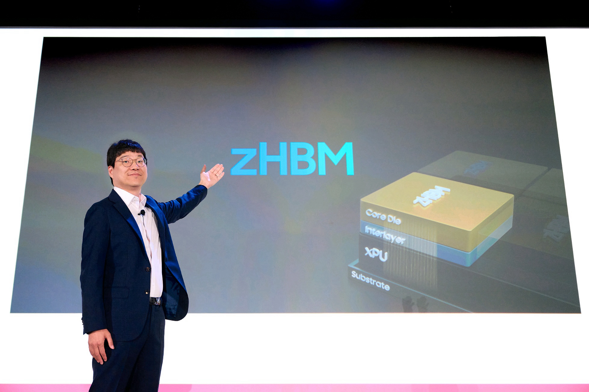
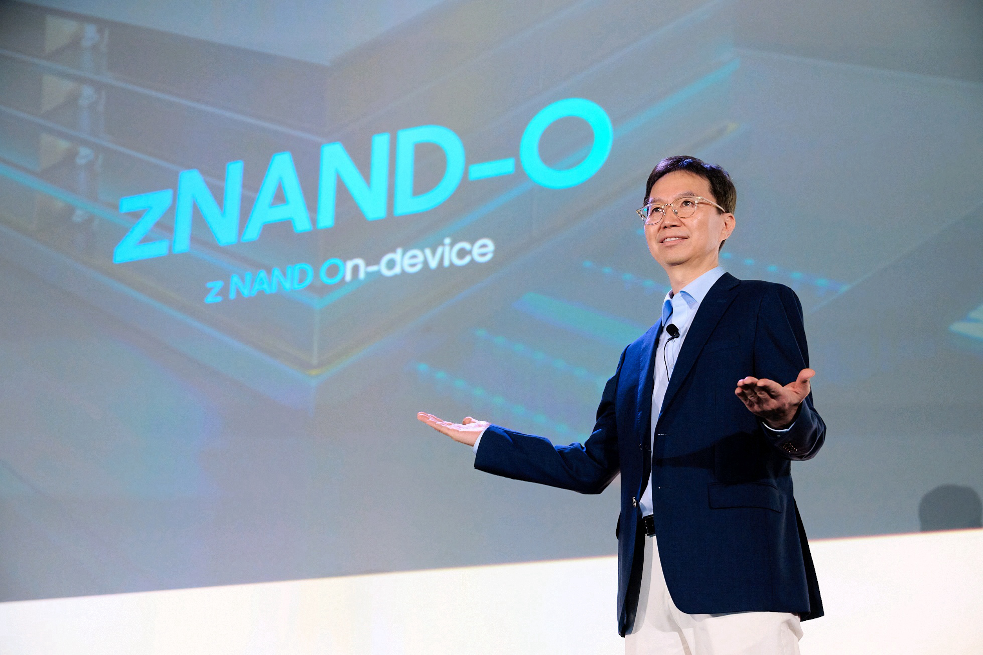
This week, Samsung presented its vision for next-generation memory and storage solutions both for AI and general-purpose applications at the Future of Memory and Storage (FMS) 2026 conference. The company introduced zHBM, zNAND-O, and BV-NAND technologies at the event, and while they are aimed at very different applications, they share one common ingredient: they all rely on wafer bonding.
Here's a breakdown of each type of technology that the company announced.
zHBM: Samsung’s vision for custom HBM ultra-high-performance memory that will sit on top of logic dies.
zNAND-O: NAND memory that can be bonded atop a logic device to maximize bandwidth, reduce latency, and minimize power consumption.
BV-NAND (aka Samsung’s 10th Generation V-NAND): Samsung’s take on bonding NAND arrays atop all the circuitry needed to operate them. This is essentially next-generation 3D NAND technology that is used today by almost everyone, including Kioxia/Sandisk, SK Hynix, and YMTC (which was the first company to adopt such a method).
This article is a preview of the type of content that readers can expect from our subscription service, Tom's Hardware Premium. If you're interested in more technical content that spans across the hardware industry, subscribe for as little as $29 per year, or $7 per month.
Don’t miss out on this Tom’s Hardware Premium. Get a full year of access for just $29, or from $7 per month. Get daily news analysis, deep dives into specialist topics in the semiconductor industry, as well as access to Bench, the largest benchmarking database around.View Deal
zHBM: Placing HBM stack on top of logic
Around the time we first heard about HBM4's 2,048-bit interface, we read a 'semi-official' report that SK hynix and its partners were considering vertical integration of HBM4 stacks on top of logic chips. To a large degree, companies were considering installing these memory stacks on top of their processors as they doubted that it would be possible and feasible to use interposers to connect HBM4 stacks to AI accelerators. Over time, it turned out that integration of memory on top of logic is complicated when it comes to cooling, power delivery, and developing interposers that can handle a 2,048-bit memory interface. Samsung's zHBM appears to be a continuation of that effort.
(Image credit: Samsung)
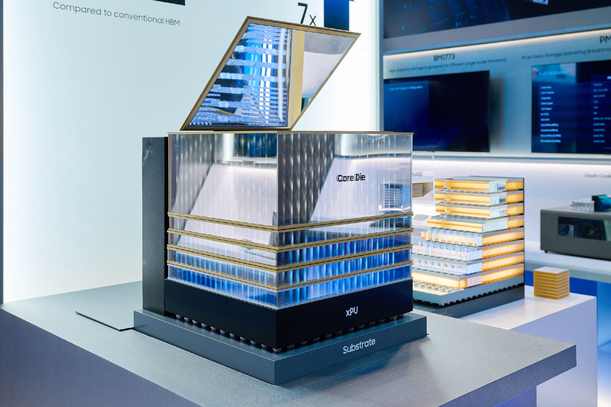
Samsung's zHBM concept places HBM directly on top of an AI accelerator instead of on its perimeter, which greatly reduces the distance data must travel between compute and memory. The company says this architecture can increase bandwidth and power efficiency and projects that it can provide 8x the 'performance of HBM5', while its advanced wafer bonding is expected to enable over 10x higher memory density, 3x better energy efficiency, and more than 50% lower thermal resistance than HBM5.
While Samsung's claims about the zHBM look incredibly impressive, they are vague. For example, when the company claims that a 'next-generation interface system incorporating zHBM' will deliver 'approximately eight times the performance of HBM5,' it never explicitly states whether this refers to memory bandwidth, actual application performance due to a combination of improvements over standard HBM, or something else. Had Samsung intended to compare raw bandwidth, it would likely have used more precise wording, such as '8x higher bandwidth.'
Instead, the general term 'performance' may have many meanings. The same applies to references of improved power efficiency, higher memory density, and lower thermal resistance compared to HBM5, a standard that has not been fully defined or ratified. To make matters even more imprecise, Samsung mentions thermal resistance, which depends on implementation rather than the standard. Finally, Samsung didn't reveal which die stacking/bonding technology it will use for zHBM.
In any case, Samsung says that zHBM will also support customer-specific designs and will enable custom IP to be integrated into the interconnect layer (which plays a role similar to the base die, though it is definitely not a base die per se) between the HBM stack and the AI processor, which essentially means that zHBM is not necessarily an industry-standard solution, so it might be implemented with additional perks.
For now, Samsung hasn't disclosed any timeframes for when it plans to offer its zHBM solutions. The only clue is that it compares it to HBM5, which is likely to see the light of day sometime in the late 2020s or early 2030s.
zNAND-O(on-device): Put storage close to compute
Samsung also unveiled zNAND-O, a high-performance NAND memory currently in development that will enable putting four or eight stacks of NAND devices on top of logic dies. zNAND-O(n) device is based on the company's V-NAND platform (or rather, BV-NAND) and is meant to combine high storage density with improved I/O performance and low latency.
(Image credit: Samsung)
Samsung claims that the tech is suitable for edge AI systems running real-time, data-intensive inference workloads, though, of course, there are many other applications that can benefit from high-performance on-package storage.
(Image credit: Samsung)
Since the technology is in development, Samsung hasn't shared much information about it, even keeping the schematics of how it plans to put zNAND-O layers on top of a logic under wraps. We can speculate that since Samsung mentions 'improved I/O performance and low-latency,' it may be planning to exploit both the inherently parallel architecture of NAND memory with a high-performance interface, though we will not try to dive into details for the sake of not making the discussion too speculative.
BV-NAND: Good old V-NAND gets a new treatment
With BV-NAND, Samsung is essentially introducing a new brand name for its next-generation 3D NAND that bonds the NAND array on top of the I/O and logic wafer. This, in turn, produces the layer itself using high-performance logic process technologies and enables higher I/O speeds.
(Image credit: Samsung)
Samsung formally announced its 400-layer-class V-NAND (aka 10th Generation V-NAND) some time ago, and even disclosed that its areal density would be 28 Gb/mm2 with a maximum I/O speed reaching 5600 MT/s. This likely stipulates the usage of a pinout that is different from the 3D NAND packages used today. While the areal density of Samsung's 10th Gen TLC V-NAND is slightly lower when compared to that of Kioxia/Sandisk's BiCS10 TLC NAND, its maximum I/O speed is significantly higher, which perhaps justifies the new branding.
NAND Layer Counts
Samsung
Samsung
Sandisk/Kioxia
Sandisk/Kioxia
Kioxia/Sandisk
Micron
SK hynix
YMTC
YMTC
Generation
V10
V9
BiCS10
BiCS10
BiCS 8
Gen 9 (G9)
Gen 9
?
Xtacking 3.0/Gen 4
Layers
4xx-Layer
290-Layer (?)
332-Layer
332-Layer
218-Layer
276-Layer
321-Layer
232-Layer
232-Layer
Density
28 Gb mm^2
17 Gb mm^2
>37 Gb/mm^2
>29 Gb/mm^2
22.9 Gb mm^2 (?)
21.0 Gb mm^2
20 mm^2
>20 Gb mm^2
19.8 Gb mm^2
Architecture
TLC
TLC
QLC
TLC
QLC
TLC
TLC
TLC
QLC
Die Capacity
1 Tb
1 Tb
?
1 Tb
2 Tb
1 Tb
1 Tb
1 Tb
1 Tb
I/O Speed
Up to 5600 MT/s
Up to 3200 MT/s
Up to 4800 MT/s
Up to 4800 MT/s
Up to 3600 MT/s
Up to 3600 MT/s
?
?
?
Considering the fact that Samsung rarely sells its memory to third parties and prefers to market client SSDs itself, a new brand for memory can be a sales driver, even if actual high-end drive performance is limited by a PCIe 5.0 x4 interface rather than by 3D NAND memory I/O. Then again, the performance of mid-range PCIe Gen5 SSDs that rely on a quad-channel NAND controller depends on 3D NAND I/O today, so marketing them under a new flash memory brand is a certain way to attract attention and then sell decent performance.
Samsung's new brand strategy
As the new name of the FMS tradeshow implies, the announcements touch upon very distinct industry needs. In the case of Samsung, we are talking about high-performance data center-grade AI accelerators; applications that need storage with latency that is lower than ~50 – 60 µs of modern high-end PCIe SSDs, though we will see how it compares to Z-NAND, and essentially a new generation of conventional 3D NAND with a new brand.
Except for the 400-layer-class Samsung BV-NAND that is set to hit the market in the foreseeable future, the company's new tech, like zHBM and zNAND-O, is years away.
Google was among the first hyperscalers to develop its own custom AI processors about a decade ago and has been steadily ramping their deployment since then. The company seems to be so confident about its TPU v9 due in 2028 that it intends to order 12 – 15 million of such processors, according to a Fubon Research note to clients published by Sean. If the information is correct, Google may not only produce more or a comparable number of AI accelerators than Nvidia, but may also need to use Intel Foundry to meet its goals.
"Based on our checks, Google plans to have 12 – 15 million TPUs in 2028," the paper reads. "Entering 2028, Google’s TPUs will enter the V9 generation with four compute dies, suggesting that their capacity consumption will more than double in 2028 versus 2027."
Fubon estimates that Nvidia supplied 8.2 million data center AI GPUs in 2026 and is on track to increase the number to 12.4 million in 2028. If Fubon is correct about Google's plans to produce 12 – 15 million 9th-generation TPUs in 2028, then the company may produce more, or at least a comparable number of AI accelerators, than Nvidia in 2028.
TSMC is not enough
How the performance of Google's v9 TPUs will stack against Nvidia's Rubin and Rubin Ultra is something that remains to be seen, but the fact that Google intends to use four compute chiplets on these AI accelerators clearly points to the fact that the company bets big on the performance of these processors. Meanwhile, building an AI accelerator with four large compute chiplets is a major engineering effort, which Google seems to have accomplished.
"Although we do not have the detailed allocation yet, we think it is difficult to reach Google’s target with TSMC alone, and Intel's supply is a must by 2028," the paper continues.
Researchers from Fubon are not sure whether Google's allocations at TSMC will be enough to meet the company's demand for 12 – 15 million 9th Generation TPUs, so they think that Google will have to use Intel Foundry's capacity to meet its volume goals. Over the past few months, we have seen reports claiming that Intel had landed orders to make three million TPUs for Google following months of Google's testing of Intel's advanced packaging technologies. Indeed, if Google wants to make its silicon at Intel Foundry, usage of Intel's advanced packaging services makes great sense. It should be noted that when compute chiplets are developed, they must be developed with their packaging technology in mind, as Intel's EMIB/EMIB-T and TSMC's CoWoS-L are incompatible.
World's largest consumer of AI accelerators
If the information about Google's plans to produce 12 – 15 million TPUs in 2028 is correct (note that the difference between 12 and 15 is 20%, which is huge) and Google will indeed deploy more AI accelerators annually than Nvidia sells to the entire market, it would mark a dramatic shift in the AI hardware landscape. It will not only make Google the world's largest consumer of AI accelerators (as the company will unlikely cease buying Nvidia hardware), it will eventually make Google the owner of the world's most capable AI hardware fleet. Whether or not Google will use its overwhelming AI compute capacity primarily for its own services, or will lend the majority to other is something that remains to be seen.
Meanwhile, for Google's rivals, the milestone will underscore the growing importance of vertically integrated AI infrastructure, where cloud providers design chips tailored to their own software stacks, workloads, and data centers instead of purchasing off-the-shelf GPUs.
Yet, Google's surpassing Nvidia in unit shipments would not necessarily diminish Nvidia's dominant position. AI demand continues to expand so rapidly that both companies could increase deployments simultaneously, but Google will simply grow faster, at least till Nvidia ups production of its AI accelerators with Feynman and Feynman Ultra in 2029 – 2030. After all, Nvidia's AI GPUs are sold out. What Nvidia should worry about is not the volumes of TPUs that Google can deploy, but rather the fact that these processors do rely on a software stack that rivals Nvidia's CUDA, the company's main competitive advantage.

 Login