❌

Normal view

Windows 11 can now reinstall itself from the cloud — Cloud Rebuild revives dead systems without secondary boot media, wipes broken installation and downloads a fresh copy of the OS

Microsoft has finally solved one of the biggest pain points of Windows with the rollout of Cloud Rebuild. The new recovery feature can reinstall Windows 11 even when an existing Windows installation is corrupt or refuses to boot. Available as a beta through the newly released Windows 11 Insider Beta Preview Build 26220.9343, the feature is essentially a hassle-free alternative to creating a Windows installation USB drive when a PC needs to be recovered.

According to Microsoft, Cloud Rebuild is designed to restore a Windows 11 PC to a “clean, known-good state” by downloading a fresh image of Windows along with the required drivers directly through Windows Update. Unlike the existing Reset this PC functionality, it does not depend on the health of your existing Windows installation, nor does it require users to have a USB drive or custom recovery image available.

The Cloud rebuild feature available in Windows Recovery

(Image credit: Microsoft)

Available via the Windows Recovery Environment (WinRE), users can access it by selecting Troubleshoot > Recovery and uninstall > Cloud rebuild from WinRE. Speaking of which, Microsoft has also improved networking support in WinRE. The recovery environment can now reuse eligible Wi-Fi profiles saved within an existing Windows installation, allowing a PC to connect during recovery without requiring administrators to separately configure Wi-Fi credentials in WinRE. Once the PC is connected, Cloud Rebuild checks Windows Update for the target Windows build and downloads the required files. Users can then confirm the Windows edition, language, and build before starting the reinstall.

The only catch here is that Cloud Rebuild completely wipes the system drive, meaning that the process removes all data stored in your main installation or C: drive, including locally stored files, accounts, applications, and settings, before reinstalling Windows. Thus, it is recommended to back up all your important files either locally or using a cloud-based service before starting the process. Once the installation is complete, the PC boots into the Windows out-of-box experience, similar to a fresh installation of Windows. For admin-managed PCs using Windows Autopilot and Microsoft Intune, the system can automatically reconnect to the organization's management infrastructure and restore assigned applications, policies, and backed-up settings.

Cloud Rebuild could particularly be useful when Windows becomes too corrupted to boot normally. Instead of finding another PC, creating installation media, and manually reinstalling Windows, users can potentially perform the entire recovery process directly from WinRE. The feature is still in preview; however, we can expect a wider release later this year.

Qualcomm’s next Snapdragon mobile chip comes into focus with on-device AI

10 September 2026 at 14:01

Qualcomm is taking an unusual approach to the launch of its next-generation premium Snapdragon mobile platform this year. Instead of holding everything for its annual Snapdragon Summit in Maui happening later this month, the company has been methodically disclosing the architecture that will power the next wave of flagship Android phones over the past couple of weeks.

First, the company disclosed its new Oryon CPU architecture, followed by a major overhaul of its Adreno GPU. Today, Qualcomm is detailing the next-generation Hexagon NPU that will serve as the platform’s primary AI engine.

Taken together, the disclosures give us a pretty good picture of where Qualcomm is going before we even know the chip’s official name.

There is obviously a strong performance story here, anchored by a 5GHz CPU, but the more interesting theme running through the architecture is memory locality and specialized AI acceleration. Qualcomm is trying to keep more data close to the compute resources that need it, while distributing AI workloads across the CPU, GPU and NPU.

These architectural changes are important as the company continues to drive on-device AI beyond relatively simple generative features toward more persistent, agentic workloads.

Oryon hits 5GHz, bolstered by FlexCache

Qualcomm disclosed in August that its next Oryon CPU will be the first mobile CPU to reach 5GHz. The eight-core design includes two 5GHz Prime cores and six Performance cores, with Qualcomm attributing the frequency gains to its fully custom Oryon microarchitecture, an in-house Arm-based CPU design that gives the company full control over the cores, cache and memory hierarchy, branch prediction and CPU subsystem.

The 5GHz headline is certainly going to get attention. However, Qualcomm’s new FlexCache architecture may ultimately have a larger impact on sustained performance. FlexCache allows Oryon’s Prime and Performance cores to tap into the same shared cache pool, with capacity dynamically allocated based on the workload. So rather than a demanding core being limited to a fixed slice of cache, it can draw on more of the available pool when needed. This keeps larger working data sets close to the CPU cores and reduces high-latency trips out to system memory.

This approach should benefit everything from gaming and multitasking to content creation, but it also aligns well with agentic AI workloads, where tasks may move through several stages of processing and across different CPU cores. The basic goal is straightforward: keep the CPU fed and avoid expensive trips to external memory.

Qualcomm’s next-gen Adreno GPU adds dedicated AI engines

Qualcomm’s next disclosure focused on graphics, where the company is making one of the more significant changes to its Adreno GPU engine in recent years. The new GPU adds dedicated Adreno Matrix Cores for running AI models directly inside the graphics pipeline. They’re paired with 18MB of Adreno High-Performance Memory, or HPM, which provides low-latency local storage for tile-based rendering, frame buffers and GPU compute.

Qualcomm claims HPM provides a 12% power improvement compared to its previous-gen Snapdragon 8 Elite Gen 5.

The more visible feature for users, however, may be Adreno Neural Fusion, which combines AI super resolution, neural processing and frame generation in a unified graphics pipeline. There are obvious parallels here to what NVIDIA, AMD and others are doing with neural rendering on the PC, though Qualcomm’s next-gen Snapdragon SoC has to operate within a much tighter mobile power envelope.

Qualcomm claims enabling Neural Fusion reduces power consumption by up to 40% in its internal testing using the company’s Dragon Alley graphics demo. That’s an impressive number, though as always, we’ll want to see how the technology behaves across actual shipping games and devices before drawing any definitive conclusions.

Qualcomm has also helped integrate Neural Fusion technology into Unity and Unreal Engine, which may ultimately be just as important as the underlying hardware. Developer adoption determines whether features like this become meaningful platform advantages or just another tick box on a spec sheet.

Qualcomm’s Hexagon NPU is being reworked for agentic AI

Qualcomm Snapdragon at work: The agentic loop, drawn on the die.

Qualcomm

The most recent disclosure centers on Qualcomm’s Hexagon NPU, where the broader architecture starts to come together. The company’s next-generation Hexagon introduces a new Element Accelerator designed for transformer workloads, alongside its existing vector and scalar processing resources. Qualcomm says the new block is optimized for fast action loops, key-value (KV) cache acceleration and context lengths of up to 32K.

Hexagon is also getting 50% more shared memory, and again, that memory complement is important. Model state, context and KV-cache data can generate substantial memory traffic, particularly with larger language models. Keeping more of that data close to the NPU can reduce latency and power consumption. Qualcomm says the architecture is designed for long-context reasoning, multimodal models, concurrent agents and low-latency action loops.

For INT4 quantized models, the company claims up to a 50% improvement in pre-fill performance versus its previous-generation Snapdragon 8 Elite Gen 5. Qualcomm is also targeting Mixture-of-Experts, or MoE, models as large as 30 billion parameters. In its example, the company points to a 30B model that activates only about 3 billion parameters during a given token-generation step. That selective approach is a natural fit for the tight power and memory constraints of a handset.

Qualcomm isn’t suggesting that a smartphone will simply run a 30B dense model entirely from DRAM, however. By activating only the experts needed for a particular task, MoE architectures can dramatically reduce active compute and memory bandwidth requirements, potentially making much larger classes of AI models practical on mobile hardware.

Qualcomm’s next-gen Snapdragon mobile impact

There is a larger competitive story here as well. For years, flagship smartphone competition largely came down to CPU, GPU, modem performance and power efficiency. AI is now another major area of differentiation, and Qualcomm is clearly designing its next-gen Snapdragon mobile platform around this need.

Apple has the advantage of controlling its silicon, operating system and software stack end-to-end. MediaTek continues to push aggressively into premium Android devices as well. Qualcomm’s response is to make its custom Oryon CPU, Adreno GPU and Hexagon NPU work more like a fully integrated compute platform, tuned for modern AI and agentic workloads.

This is a solid advantage for Android handset OEMs because many don’t have the resources to engineer this level of silicon integration themselves. Qualcomm can effectively provide its Android OEM partners, including Samsung, Xiaomi, Honor and others, with a common hardware foundation for on-device AI, advanced graphics and agentic computing. It also gives Qualcomm another way to defend its premium Snapdragon position.

The company’s custom Oryon architecture now spans smartphones and Windows PCs, and soon servers, while AI acceleration is distributed across its CPU, GPU and NPU. For business users, that could mean more AI processing happens locally, reducing cloud and network dependence, improving response times and keeping more potentially sensitive data on-device. And for IT organizations, Qualcomm now has an opportunity to provide a more consistent AI compute foundation across Windows PCs with Snapdragon X and premium Android handsets.

There is still plenty we don’t know, however. Qualcomm hasn’t disclosed the complete SoC specifications, final performance or power characteristics, or which devices will ship with it initially. Many of these AI experiences will also depend heavily on Android, app developers and the models themselves.

The new 5GHz mobile CPU may generate the biggest headline at Snapdragon Summit, but the more important developments may be what sit around it: more local memory, specialized AI acceleration and tighter integration between the CPU, GPU and NPU.

If Qualcomm can translate this architecture into better sustained performance, enhanced power efficiency and useful on-device AI experiences, it could strengthen its position in premium Android phones while putting more competitive pressure on Apple. For business users, the payoff could be more capable local AI without sacrificing the performance and battery life expected of a flagship device.

That is the part I’ll be watching most closely when the complete silicon picture is unveiled at Snapdragon Summit later this month. And I may even get some hands-on time with it in some benchmarks, as we have in years past, so we shall see.

d-Matrix drinks the Nvidia Kool-Aid with NVLink Fusion and MGX rack designs

10 September 2026 at 14:00
AI infrastructure startup d-Matrix on Thursday joined the growing list of chipmakers licensing Nvidia’s NVLink Fusion interconnect tech and rack-scale reference designs to make its high-performance inference platform more accessible to customers. Under the deal, d-Matrix will integrate support for NVLink Fusion, a high-speed chip-to-chip interconnect that Nvidia began licensing last year, into future chip designs, including its upcoming Raptor accelerators. As we’ve previously reported, by embracing the tech, d-Matrix sidesteps many of the challenges associated with scaling its chip architecture across large compute clusters. By using NVLink over alternative interconnects and designing its compute blades around the GPU giant’s MGX reference designs, its customers can deploy its chips using the same racks and NVSwitch fabrics as Nvidia. By the end of next year, d-Matrix expects to offer systems with up to 144 Raptor accelerators connected by a single all-to-all NVLink fabric. While there’s a lot we don’t know about Raptor just yet, at the Hot Chips conference last month the company revealed each Raptor “card” would feature 32 GB of ultra-fast 3D-stacked DRAM on board capable of delivering 100 TB/s of memory bandwidth — roughly 4.5 times the memory bandwidth of Nvidia’s Rubin GPU. By the looks of things, the XPUs that will power d-Matrix's NVL144 racks are about half the size of the Raptor cards shown off at Hot Chips and include around 16 GB of 3D-DRAM and about 50 TB/s of memory bandwidth — still quite respectable by any measure. With 144 of these per rack, d-Matrix is looking at about 2.3 TB of memory capacity — enough for models exceeding four trillion parameters in size at 4-bit precision — and about 7.2 petabytes a second of peak aggregate memory bandwidth. This is achieved by bonding compute logic atop a stack of DRAM. The result is an in-memory compute platform that offers modest capacity while maintaining memory bandwidth closer to that of SRAM than is achievable using HBM. Memory bandwidth, as you may recall, is the biggest bottleneck for AI inference. The faster your memory, the faster the system can spew out tokens. This is exactly why Nvidia dropped $20 billion last year to license Groq’s IP and hire away its engineering talent. The chip’s SRAM-heavy dataflow architecture was capable of hitting 150 TB/s per chip, but the tradeoff is that SRAM isn’t very space-efficient and the chipmaker could only pack 500 MB of it onto a single die. d-Matrix's Raptor promises to deliver a decent fraction of that bandwidth with 64x higher capacity, which means the company can get away with using far fewer chips per model. Where a trillion-parameter model might need more than 2,000 Groq 3 LPUs at 8-bit precision, a single d-Matrix system would only need about 64 (32 at 4-bit precision). Just like Groq’s LPUs, d-Matrix chips can be deployed standalone, or as part of a heterogeneous compute config using GPUs for the compute-intensive prompt processing (prefill) phase of the inference pipeline and its Raptor accelerators for the memory bandwidth bound token generation (decode) phase. And for enterprises interested in the ultra-low latency inference capabilities of Groq, d-Matrix’s chips may offer a cheaper point of entry since fewer XPUs would be required. Nvidia’s walled garden We looked at Nvidia’s emerging IP licensing strategy in more detail last week, but in a nutshell, Nvidia stands to gain a lot more than licensing revenues from NVLink Fusion adopters. In addition to licensing Nvidia’s interconnect tech, d-Matrix plans to pair its accelerators with the GPU giant’s Vera CPUs, NVSwitch appliances, BlueField and ConnectX NICs, and SpectrumX Ethernet products. In other words, Nvidia stands to make a lot of money even if it’s not selling GPUs. It seems a fair number of chip designers are willing to make that kind of deal to avoid having to design their scale up networks or rack systems. Last week, MediaTek joined Marvell, Qualcomm, Arm, Fujitsu, and Amazon Web Services in adopting Nvidia’s NVLink Fusion interconnects. Nvidia is so invested in getting folks into its walled garden that it's spending billions on incentives to get them in the door. As part of the MediaTek deal last week, Nvidia invested $3.5 billion in the SoC designer, while it spent $2 billion to get Marvell in the door. No word on whether the latest deal included any such terms. ®

Dominant tree pollen shapes nutrient levels in European forest throughfall

10 September 2026 at 12:52

Every spring, Europe’s forests are showered with far more than rain. Wind-pollinated trees release staggering quantities of pollen into the atmosphere, and much of it eventually settles on leaves, branches and the forest floor. New research now shows that this pollen is not merely biological debris — it is a measurable, taxon-specific driver of nutrient fluxes in the water that drips through forest canopies, a flow scientists call throughfall. The findings, published in Environmental Monitoring and Assessment, provide the first continental-scale evidence directly linking pollen deposition to forest water chemistry, and they suggest that decades of forest monitoring may have been quietly misattributing a slice of nutrient input to other sources.

The study was carried out by a large international team led by Elena Gottardini of the Fondazione Edmund Mach in Italy, working within the ICP Forests programme, a pan-European network that monitors air pollution effects on forests. The researchers analysed throughfall samples collected in 2018 from 60 intensive monitoring plots — known as Level II plots — across eight countries: Belgium, Finland, France, Germany, Italy, Norway, Switzerland and the United Kingdom. The plots ranged in altitude from 14 to 1,900 metres above sea level and were dominated by six tree genera: Abies, Fagus, Larix, Picea, Pinus and Quercus. In total, 196 throughfall samples were collected between February and July, covering the early vegetative season when most European trees flower.

The innovation of the study lies in its methodology. Rather than inferring pollen inputs from nearby aerobiological samplers, the team examined the very same water samples that were being chemically analysed. A known quantity of water from each sample was filtered through a 5-micrometre cellulose nitrate mesh, and a calibrated number of 10-micrometre polystyrene-divinylbenzene microspheres — roughly 155,000 per sample — were added as a counting standard. The filters were then dissolved in acetone, centrifuged, and the resulting pellet embedded in fuchsin jelly on microscope slides. Trained analysts identified and counted pollen grains under 400-times magnification, stopping when about 1 percent of the added microspheres had been counted. From these counts, the team calculated pollen deposition rates in grains per square metre per day, correcting for filtered volume, throughfall quantity and sampling duration.

The results were striking. Fifty-three pollen taxa were identified across the samples, with woody species accounting for 98 percent of all grains. Four genera — Pinus, Picea, Fagus and Quercus — together made up 91.4 percent of the total. Pine pollen alone represented more than half of everything collected, a dominance the researchers attribute to the buoyant air sacs on pine grains, which allow them to travel enormous distances from both local and distant sources. In beech, spruce and pine stands, the pollen of the dominant genus itself prevailed, making up 49.7, 59.1 and 84.3 percent of the local pollen spectrum respectively. In oak stands, oak pollen ranked second at 26.9 percent, behind pine. Data from fir and larch stands were excluded because sampling there did not align with those genera’s flowering periods.

By combining the measured pollen curves with published flowering phenology, the team defined main pollen seasons for each genus. Beech and oak flowering spanned April and May, with beech peaking in the last week of April and oak showing a double peak at weeks 19 and 23, likely reflecting multiple oak species flowering at slightly different times across the wide latitudinal and altitudinal spread of plots. Spruce pollen peaked around weeks 19 to 20, while pine peaked at week 19 with a secondary pulse at week 22. Overall, 57 percent of the throughfall samples fell within their stand’s flowering period for at least half of their collection window, providing a robust temporal overlap between pollen deposition and water chemistry measurements.

The chemical analysis, conducted at the Research Institute for Nature and Forest laboratory in Belgium, quantified major ions including potassium, calcium, magnesium, sodium, chloride, phosphate, sulphate, nitrate, nitrite and ammonium using ion chromatography, alongside total dissolved nitrogen and non-purgeable organic carbon measured on a TOC/TN analyser. Linear mixed-effects models then tested whether pollen deposition rates could predict the flux of these compounds, with plot identity included as a random effect and autocorrelation between repeated samples explicitly modelled.

The answer was a clear yes. Every statistically significant association between pollen and throughfall chemistry was positive, meaning more pollen corresponded to more nutrients reaching the forest floor. Potassium emerged as the star player: its flux was significantly explained by pollen from all four main genera, with pollen accounting for an average of 33 percent of the variance. This makes biochemical sense, because potassium is one of the predominant ions in pollen grains, and pollen washed from flowers and crowns by rain or deposited dry is a direct source of the ion during the flowering season — an idea first proposed decades ago but never confirmed at this scale. The strongest single relationships involved oak pollen, which explained 77.8 percent of the variance in ammonium fluxes and 55 percent in total dissolved nitrogen.

Broadleaved and coniferous pollen left different chemical fingerprints. Beech and oak pollen together significantly explained fluxes of non-purgeable organic carbon, dissolved organic nitrogen, total dissolved nitrogen, ammonium and magnesium, while the combined pollen of pine and spruce was linked with every measured compound except phosphate. Intriguingly, broadleaved pollen showed a weak negative association with nitrate fluxes. The authors urge caution in interpreting this pattern, since several non-exclusive mechanisms could be at play. Laboratory experiments have shown that pollen and its associated microbiota can transform extracellular nitrate into nitrite and nitrous oxide, an effect pronounced in beech and oak but weak or absent in pine and spruce. Canopy uptake of nitrogen and coincidentally lower atmospheric deposition during broadleaf flowering are also possible explanations that this single-year study cannot disentangle.

The dissolved organic carbon carried in throughfall also differed by forest type. Specific ultraviolet absorbance at 254 nanometres, a proxy for aromatic and recalcitrant carbon, was highest in spruce stands, whose needles release lignin derivatives and tannins. The humification index was significantly higher in oak throughfall, reflecting more decomposed, humic organic matter. Most revealing was the fluorescence index, which distinguishes microbial from plant-derived organic matter: beech and oak samples had significantly higher values, with medians near 1.9, than pine and spruce samples, which sat near 1.7. Values above 1.9 typically indicate microbially processed carbon, and the elevated readings under broadleaves suggest microbes play a larger role in transforming pollen-derived carbon in those forests — hinting that pollen inputs feed not just trees but entire soil microbial food webs.

For the authors, the implications reach well beyond academic curiosity. Routine throughfall monitoring has historically ignored pollen as a variable, meaning that chemical enrichment previously attributed solely to canopy leaching or atmospheric deposition may in fact be partly pollenic. As climate change pushes flowering earlier and increases airborne pollen amounts across arboreal taxa, these hidden inputs could grow. Masting behaviour in beech and oak — the episodic, synchronized production of enormous seed and pollen crops — introduces strong year-to-year variability that any nutrient budget must now reckon with.

The researchers acknowledge the limitations of a one-year, correlative dataset and call for multi-year studies incorporating canopy architecture, stand age, phenology and insect infestations, as well as stable isotope tracing or controlled exclusion experiments to nail down mechanisms. Still, the message is clear: pollen is not just about reproduction, or even allergies. It is a seasonal fertiliser delivered from the sky, and forests have been banking on it all along. Incorporating pollen surveys into long-term forest observation networks, the team argues, will be essential for accurate nutrient budgets in a changing climate.

Subject of Research: The influence of deposited tree pollen on the nutrient composition of throughfall in European forests

Article Title: Deposited pollen from dominant tree genera drives nutrient composition of throughfall in European forests

Article References: Gottardini, E., Cristofolini, F., Cristofori, A., Vanguelova, E., Thimonier, A., Clarke, N., Wachtveitl, L., Ukonmaanaho, L., Lindroos, A.-J., Nicolas, M., Limić, I., Boeckx, P., Bodé, S., Bauters, M., & Verstraeten, A. (2026). Deposited pollen from dominant tree genera drives nutrient composition of throughfall in European forests. Environmental Monitoring and Assessment, 198(10), Article 1053. https://doi.org/10.1007/s10661-026-15883-0

Image Credits: AI Generated

DOI: 10.1007/s10661-026-15883-0

Keywords: Tree pollen deposition, Throughfall chemistry, Atmospheric deposition, Forest nutrient cycle, Potassium fluxes, Dissolved organic carbon, ICP Forests, Flowering phenology, Nitrogen cycling, European forests

Reducing earthquakes caused by fracking

10 September 2026 at 12:00

Drilling for electricity or geothermal energy is a common human-caused source of earthquakes. Drillers or engineers inject water into the earth to fracture underground rock through a process known as fracking. This allows scientists to produce clean energy almost anywhere on Earth by heating up water in the cracks using facilities called enhanced geothermal systems or EGS plants. However, fracking causes earthquakes, which are a major concern for people’s safety globally. Therefore, scientists are looking for new fracking methods that cause fewer earthquakes.

Fracking for EGS plants can trigger earthquakes by changing the pressure underground and adding stress to the surrounding rock. However, these earthquakes happen at pre-existing, naturally occurring cracks called faults, which are different from the newly formed, man-made cracks. Faults are naturally under pressure from the overlying rock and the surrounding earth since they reach deep underground. As pressure builds up over time, it eventually causes the rocks to shift along these faults and release energy in the form of earthquakes. 

During fracking, engineers use 4 different shut-in strategies to finish off water pumping. The standard industry strategy is called instant shut-in, where the injection pump is turned off immediately, but the water stays underground, causing the pressure to lower naturally. In a similar strategy, known as the tapered shut-in, engineers gradually reduce the water injection rate to zero instead of immediately turning it off. For the high-rate and low-rate extraction strategies, they pump the water back out after injection is complete, at different pump rates.

Recently, scientists aimed to mitigate the risk of earthquakes by testing these 4 shut-in strategies to determine which is most effective. They compared the shut-in strategies using crystalline basement rock with low porosity and permeability, meaning water couldn’t easily flow through it. Engineers use this same type of rock for EGS plants so they can control where the water flows. The scientists pumped water into the rock, then measured the pressure and stress levels where rocks began to move along faults, determining the point at which earthquakes would occur. 

The scientists applied high-rate and low-rate extraction methods to the rock and found that pressure and fault movements decreased. However, when they applied instant and tapered shut-in methods to the same rock, they increased the pressure and caused continuous fault slipping. They measured stress in the rock during these methods and found that high-rate extraction stabilized the fastest, while low-rate extraction stabilized more slowly. In contrast, instant shut-in continuously increased the pressure and slip, and tapered shut-in caused the highest stress of all.

The scientists also used a computer model to simulate what happened at an EGS site in South Korea, where earthquakes occurred after injections using the instant shut-in method. They set up the model using a rock with the same characteristics, injection wells, and faults as that site. Then, they simulated periods of injection based on the previous real-world events and modeled the effects of pressure and stress to determine if the earthquakes could have been prevented. 

The team used the model to compare how a site like this would respond to the instant shut-in method versus the other shut-in methods. They found that the tapered shut-in method increased pressure and stress in the rock, while the high-rate and low-rate methods both decreased pressure and stress. The high-rate method decreased pressure and stress more than the low-rate method. 

The scientists concluded that high-rate extraction is the most effective method for reducing the risks of post-injection earthquakes during EGS fracking in crystalline basement rock. Additionally, the scientists determined that the earthquakes in South Korea could have been prevented if engineers had used either the high-rate or low-rate extraction methods. They recommend using high-rate extraction to reduce earthquakes during EGS fracking, which would allow EGS plants to generate clean energy more safely.

The post Reducing earthquakes caused by fracking appeared first on Sciworthy.

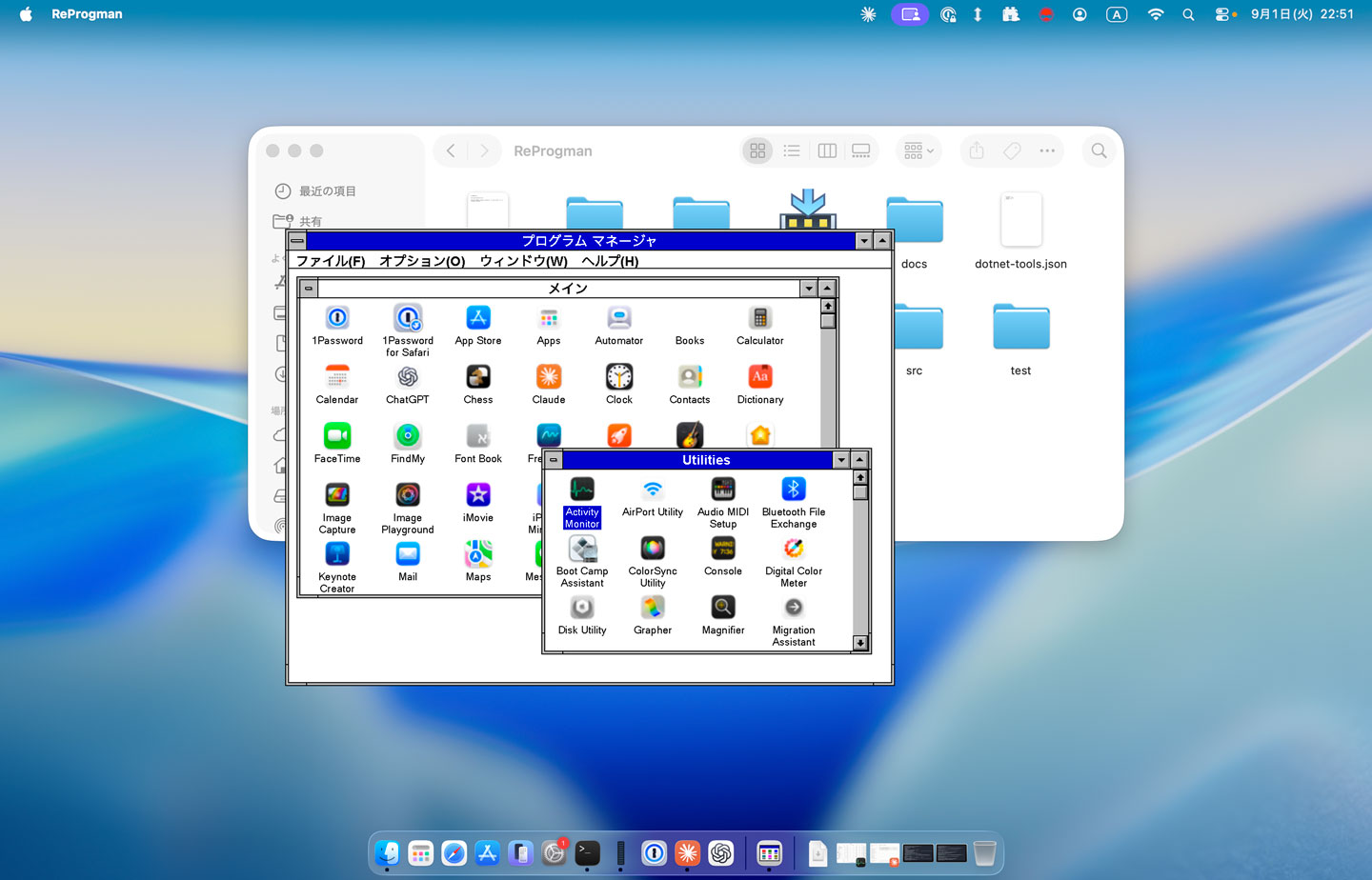
Developer uses Claude to vibe code a Windows 3.1 shell in an hour — reanimated 12MB retro launcher runs on both Windows 11 and Apple Silicon

10 September 2026 at 12:00

If you are yearning for a quick-shot retro Windows experience on your modern Windows 11 or macOS system, then there’s a new vibe-coded clone of the Windows 3.1 Program Manager that may interest you. Developer Mayuki has released a neat little nostalgia project dubbed ReProgman – named after the ancient Windows 3.1 ‘progman.exe ’, which was the primary shell of the era – until Windows 95 swept it away three decades ago.

ReProgman macOS screenshot

ReProgman macOS screenshot (Image credit: Developer Mayuki on GitHub)

ReProgman looks pretty authentic to my eyes, and it brought back memories of why I wasn’t sad to see it shrivel away from Windows machines. In a social media post about the release of ReProgman, Mayuki seems to agree with my sentiments. “I asked Claude to create a clone of the Windows 3.1 Program Manager,” wrote the developer (machine translation). “I think you'll enjoy reminiscing with it for about 30 seconds.”

Claude Code worked pretty swiftly to churn out this clone of the Windows 3.1 shell. The first version that was precipitated in about an hour was “pretty decent” but needed some effort to iron out the wrinkles. Then Mayuki complains again that actually using ReProgman induced boredom after about half a minute of usage.

The end-user-ready releases of ReProgman weigh in at between 12 and 16MB, so they are quite a trivial download and don’t need installing. Thus, it isn’t very taxing to give them a try for a spot of nostalgia-tinted navigation around your present system’s programs and files. Mayuki says that building and running this application needs the .NET SDK 10.0+. The code has been released on GitHub under the MIT license.

In conclusion, Miyuki’s ReProgman provides an easy trip down personal computing's memory lane, specifically to the Windows 3.X era of the early to mid-1990s. However, some will prefer to get their retro computing kicks by running the actual MS-DOS/Windows 3.1 combo on real hardware. As we discovered recently, that doesn’t limit users to dusting off an old i486 or similar. Back in April, an enthusiast demoed Windows 3.1X on ultra-modern bare metal with a system using a Ryzen 9 9900X and RTX 5060 Ti.

Samsung to help fortify OpenAI's semiconductor supply chain

9 September 2026 at 21:18
OpenAI will design its next-generation AI accelerators with the help of South Korean foundry giant Samsung Electronics. This move could help the ChatGPT maker with memory, process tech, or other key things it needs to succeed. The announcement, made by OpenAI Korea general manager Harrison Kim in a press conference Wednesday, comes just weeks after the company showed its first-generation “Jalapeño” accelerators besting Nvidia’s Blackwell GPUs across a slew of inference workloads. "One of the areas where we have made the most progress and gained the most recognition with Samsung Electronics is our joint production and research on the next-generation chips we are developing," he said, according to Reuters. But now that the hype has died down and Wall Street has convinced themselves that the rise of AI ASICs isn’t the threat to Nvidia’s dominance they feared, OpenAI still has to contend with the realities of being a fabless chip designer. The vast majority of leading edge silicon made today comes from a single company: TSMC. That means securing meaningful capacity requires competing with AMD, Nvidia, and practically every other chip biz and hyperscaler designing their own chips. But TSMC isn’t the only leading edge wafer fab out there. They’re just the biggest. Smaller, less popular options include Samsung Electronics and Intel Foundry. The supply of high-bandwidth memory (HBM), which OpenAI’s (and Broadcom if we’re being honest here) designs make extensive use of, is similarly constrained with just three major manufacturers capable of producing it in volume: SK Hynix, Micron, and you guessed it, Samsung Electronics. This puts OpenAI in a tough spot of having to compete with larger, higher volume chip designers for both logic and memory silicon. As such, OpenAI’s tie-up with Samsung could go two ways. The most obvious, but also the least interesting, is that Samsung will supply all or at least some of the HBM used in the model dev’s next-gen chips, which we’ll call Habanero for lack of an official code name. Detailed at Hot Chips last month, OpenAI’s Jalapeño AI inference chip uses HBM4, the same tech used by AMD and Nvidia’s latest GPUs. That tells us that there's a pretty good chance Habanero will likely use the faster HBM4E. And given the ongoing memory shortage, if OpenAI wants to secure ample supply, it’s going to need to forge these relationships early. Besides supply chain, timing is important because there’s a good chance OpenAI’s next chip will take advantage of custom base dies to move things like memory controllers or even some logic from the compute silicon to the HBM stack itself. If you recall Nvidia’s disclosures around NVHBM a few weeks back, it’s the same idea. However, these custom base dies require some coordination with the HBM supplier, so fostering a close relationship with Samsung now would benefit OpenAI, even if the compute chiplets themselves end up being manufactured by TSMC. While the most obvious reason for OpenAI’s tie-up with Samsung is memory-related, that’s not to say they couldn’t fab their next chip on Samsung’s 2 nm process tech just to have an alternative supplier to TSMC. Samsung is the second largest leading edge foundry operator in the world and used to produce a lot of silicon for the likes of Nvidia, Apple and others. Nvidia’s Ampere generation used Samsung’s 8 nm process tech for the majority of its PCIe-based cards, while its HBM-equipped accelerators were exclusively fabbed by TSMC. But a number of factors, including the rise of multi-die architectures requiring advanced packaging and broader adoption of HBM-based accelerators, made TSMC the more attractive option. Reported challenges with Samsung’s yields across its 3 nm process tech probably didn’t help either. But as of 2026, Samsung is looking a lot more compelling, with chip designers including Rebellions, Tenstorrent, and Groq building sophisticated AI accelerators at its fabs. Rebellions’ Rebel100 accelerator is a particularly useful proof point as it utilizes a multi-die architecture and HBM3E, both of which require sophisticated advanced techniques to stitch everything together. The chip shows that Samsung is more than capable of producing OpenAI’s next chip. What’s more, doing so could open the door to larger allocations than they would get from TSMC alone. We reached out to OpenAI for comment on its silicon strategy, but had not heard back as of publication. ®

Popular navigation apps unlikely to ditch Mercator maps despite UN resolution

9 September 2026 at 18:11

Nearly every country represented in the United Nations General Assembly recently voted in favor of promoting world maps that more accurately show the size of various continents. But the UN resolution is unlikely to change how millions of people regularly see versions of 16th-century Mercator maps depicting skewed continent sizes in navigation apps.

On September 4, the African-led resolution attracted 164 votes in favor, with six countries abstaining from voting. Only the United States voted to oppose the resolution after describing it as a “radical ideological project,” according to UN News.

The non-binding UN resolution does not impose map changes on anyone. Instead, it “encourages governments, schools, international organizations, and technology companies to use the Equal Earth projection and other so-called equal-area maps when relative size matters,” UN News reported. The resolution also encourages teaching about the trade-offs that arise from depicting a spherical planet on a flat map.

Read full article

Comments

© UN Photo/Loey Felipe

Locking-enabled multimodal soliton microcombs achieve day-scale stability for precision metrology

9 September 2026 at 17:57

Optical frequency combs have transformed the way scientists measure light and time, earning the Nobel Prize in Physics in 2005 and underpinning technologies ranging from atomic clocks to exoplanet detection. Yet the miniature on-chip versions of these combs, known as soliton microcombs, have long suffered from a frustrating paradox: the most stable and useful operating regimes have also been the most fragile and difficult to sustain. A newly published study in Light: Science & Applications reports a significant advance toward resolving this tension. Researchers led by J. Tang, J. Yang and E. Yan describe a multimodal locking-enabled soliton microcomb that combines robust, self-starting operation with an exceptionally low repetition rate on the scale of a day of stable measurement time, opening a path toward practical high-precision metrology systems that can run unattended for extended periods.

At the heart of the advance is a technique the authors call multimodal locking, a scheme that stabilizes not just a single resonance of the optical microresonator but multiple modes simultaneously, locking the comb dynamics to a regime in which dissipative Kerr solitons can form and persist without delicate manual tuning. In conventional microcomb systems, soliton formation typically requires a precise and rapid traversal of a “chaotic” modulation instability regime, a step that is notoriously sensitive to thermal transients in the resonator chip. Laser frequency must be swept with exquisite control while the soliton’s own heat dissipation shifts the resonator’s resonances, creating a feedback loop that can destroy the soliton state within microseconds. The multimodal locking approach circumvents this fragility by engaging several mode families of the resonator at once, so that the interplay among them pins the comb to a stable soliton state even as environmental and thermal conditions fluctuate.

The significance of achieving a low repetition rate in the same device cannot be overstated. A frequency comb’s repetition rate is the spacing between its individual comb teeth, and for many applications, coarser spacing is a decisive advantage. In laser ranging and distance metrology, for example, the ambiguity range of an interferometric measurement is set by the inverse of the comb’s free spectral range. Microcombs, generated in whispering-gallery-mode or ring resonators only a few millimeters across, usually exhibit repetition rates of tens to hundreds of gigahertz, which severely limits the unambiguous measurement range available to a comb-tooth-resolved distance measurement. By engineering a low-repetition-rate soliton state, the research team extends this ambiguity range dramatically, making the microcomb directly useful for absolute distance measurement, multi-wavelength interferometry and coherent communications, where each comb line must be spectrally resolvable and addressable.

Achieving both low repetition rate and robust soliton generation in a single microresonator is a formidable engineering challenge. Low repetition rates demand large resonator diameters, which in turn produce dense spectra of resonances and increased susceptibility to mode crossings with higher-order transverse and polarization mode families. Such crossings historically destabilize soliton formation, causing comb states to collapse or preventing single-soliton operation altogether. The multimodal locking strategy turns this liability into an asset: rather than engineering mode crossings away, the researchers harness the coupling among mode families to lock the comb dynamics into a favorable basin of attraction. The result is a soliton microcomb whose low repetition rate is preserved over day-scale timeframes, a duration that places the device among the most operationally stable microcomb demonstrations reported to date.

Day-scale stability matters because it transforms the microcomb from a laboratory demonstration into an instrument. Many high-precision experiments, from astronomical spectrograph calibration to the accumulation of statistical confidence in atomic spectroscopy, require comb sources that remain locked and stable across many hours or even days of continuous operation. Conventional fiber-laser-based frequency combs achieve this, but at the cost of table-top size, high power consumption and substantial maintenance overhead. Microcombs promised to shrink the technology onto a photonic chip, yet until now their operational fragility has confined most demonstrations to short observation windows. The robust low-repetition-rate soliton microcomb described in the new work demonstrates that chip-scale frequency combs can, with appropriate locking architecture, sustain the kind of long-duration, hands-off operation that real metrology campaigns demand.

The physics underlying soliton microcombs rests on the Kerr nonlinearity of the resonator material, typically silicon nitride, magnesium fluoride or fused silica. When continuous-wave pump light resonantly builds up inside the ring, the Kerr effect produces a four-wave-mixing process that seeds sidebands spaced by the resonator’s free spectral range. Under the right conditions of pump detuning and intracavity power, these sidebands evolve into a coherent train of ultrashort optical pulses, dissipative Kerr solitons, that circulate around the resonator and emit a broadband comb spectrum with tooth spacing equal to the repetition rate. The comb’s output frequencies are determined by two radio-frequency quantities, the pump laser frequency and the repetition rate, which is why the combs can serve as rulers for measuring optical frequencies against a reference. Any drift in either quantity propagates directly into measurement error, and the multimodal locking mechanism suppresses precisely this drift by anchoring the comb’s underlying mode structure to the resonator’s intrinsic stability.

Applications for such a device span an unusually broad swath of science and engineering. In high-precision laser ranging, low-repetition-rate combs with tooth spacings in the low-gigahertz or even megahertz regime allow interferometric distance measurements over ranges of meters to kilometers without the need for auxiliary synthetic-wavelength techniques. In astronomical spectroscopy, comb calibration sources with well-controlled line spacing enable the detection of Earth-like exoplanets through radial velocity shifts measured in centimeters per second. In telecommunications, low-repetition-rate combs align naturally with standard channel grids used in wavelength-division multiplexed fiber networks, making them attractive as multi-carrier sources. In spectroscopy, dual-comb techniques benefit from repetition rates that are low enough to permit resolution of closely spaced molecular absorption features. A microcomb that is simultaneously robust, low-repetition-rate and day-scale stable therefore functions as a versatile enabling component across these domains rather than a single-purpose device.

The demonstration also speaks to a broader trend in photonics: the migration from delicate, expert-operated laboratory setups to self-contained, self-stabilizing systems. The self-starting character implied by multimodal locking is particularly important for this transition. A comb that requires a skilled operator to initiate soliton formation, sweeping the laser with practiced timing past the chaotic regime, cannot be deployed in an observatory dome, on a satellite platform or inside an industrial instrument. A comb that engages its soliton state reliably on demand and then holds it through thermal cycling, laser drift and mechanical perturbation removes the last practical barrier to integration. The authors’ demonstration of day-scale continuous operation is, in effect, a stress test passed by a technology that researchers have been attempting to harden for more than a decade.

The implications extend to metrology standards and timing as well. Optical atomic clocks, which now achieve fractional frequency uncertainties below one part in 10^18, rely on frequency combs to divide down their optical oscillations to countable microwave rates. Miniaturizing the comb stage of such clocks is a prerequisite for portable optical timekeeping, which would benefit navigation in GPS-denied environments, geodesy that monitors sea level and crustal motion with millimeter precision, and fundamental physics tests that track the constancy of natural constants over months and years. A robust chip-scale soliton microcomb with day-scale stability contributes a key subsystem to this vision, and the multimodal locking principle may generalize to other resonator platforms, materials and spectral regions, including the mid-infrared where molecular fingerprinting awaits compact comb sources.

Looking forward, the study suggests several directions that the photonics community is likely to pursue. Combining multimodal locking with on-chip pump lasers and integrated electronics would complete the transformation toward fully self-contained comb modules with no free-space optics. Extending the approach to lower repetition rates still, into the megahertz regime where fiber-laser combs operate, would bring microcombs into direct competition with their bulkier predecessors for the most demanding ranging and spectroscopy tasks. Improvements in resonator fabrication, reducing mode-volume disorder and engineering dispersion with greater precision, will further expand the parameter space in which robust soliton states can be locked. The present work demonstrates that the fragility once considered intrinsic to soliton microcombs is not a fundamental limit but an engineering problem, and one that can be solved by embracing, rather than avoiding, the multimodal structure of real optical resonators.

The research, published in Light: Science & Applications, marks a milestone in the maturation of microcomb technology. By uniting three properties that had previously been achieved only separately, self-starting robustness, low repetition rate and day-scale operational stability, the work delivers a soliton microcomb genuinely suited to high-precision metrology. As the demand for compact frequency references accelerates across navigation, astronomy, communications and fundamental science, the multimodal locking strategy reported by Tang, Yang, Yan and colleagues offers a clear and technically grounded route from chip-scale optical chaos to dependable, precision measurement light.

Subject of Research: A robust, self-starting low-repetition-rate soliton microcomb enabled by multimodal locking for day-scale-stable, high-precision metrology applications.

Article Title: Multimodal locking-enabled robust and day-scale low-repetition-rate soliton microcomb for high-precision metrology

Article References: Tang, J., Yang, J., Yan, E., Huang, G., Yin, K., Tian, D., Lei, X., Huang, J., Yang, M., Ding, H., Yan, S., Wei, K., Zhu, L., Wang, G., & Jiang, T. (2026). Multimodal locking-enabled robust and day-scale low-repetition-rate soliton microcomb for high-precision metrology. Light: Science & Applications, 15(1), Article 370. https://doi.org/10.1038/s41377-026-02460-w

Image Credits: AI Generated

DOI: 10.1038/s41377-026-02460-w

Keywords: soliton microcomb, multimodal locking, low repetition rate, frequency comb, high-precision metrology, laser ranging, day-scale stability, dissipative Kerr solitons, chip-scale photonics, optical frequency reference, self-starting comb, Light Science & Applications

Modeling framework reveals grid battery aging effects

By: Laura
9 September 2026 at 12:00
Energy storage is becoming critical to grid resilience and electricity affordability because battery systems can help balance supply

💾

Auf YouTube findest du die angesagtesten Videos und Tracks. Außerdem kannst du eigene Inhalte hochladen und mit Freunden oder gleich der ganzen Welt teilen.

Floating nuclear startup Bluecore lands $50M funding before setting sail

8 September 2026 at 17:30
Startup Bluecore Energy has raised $50 million in seed funding to develop floating nuclear power plants intended to supply ports and other locations with rapidly growing energy demands. The California-based company said the Silverton Partners-led round, which includes $10 million in previously announced pre-seed funding, brought in several new investors. It plans to use the money to engineer and test its compact nuclear power system and pursue regulatory approval and maritime classification. Its initial design is intended to generate about 10 MWe – megawatts of electrical output – continuously using light-water reactor technology. Bluecore says the maritime system would be able to operate for years at a time and require refueling only once every few years. The company has secured its first barge and is developing a non-fueled, electrically heated reactor module prototype at its Port of Long Beach headquarters to test monitoring, sensor, and control systems. Bluecore is targeting ports, AI datacenters, and coastal infrastructure, with the reactors potentially deployed offshore and connected to customers by subsea cables. Remote islands and coastal settlements in places such as Alaska may also lack practical connections to a wider electricity grid. Bluecore claims its approach could provide reliable, zero-emission power to energy-intensive locations and open additional markets for nuclear generation. "Six months ago, we were building the foundation. Today, we have the capital, the team, the hardware, and some of the most important institutions in nuclear and maritime working alongside us," said Bluecore founder and CEO Kofi Asante. "Our focus now is simple: create and deliver zero-emission energy as safely and quickly as possible." The move follows the launch of the International Atomic Energy Agency's (IAEA) Atomic Technologies Licensed for Applications at Sea (ATLAS) initiative in the US capital last month. Secretary of Energy Chris Wright linked that event to the Department of Energy's own efforts to rapidly expand the provisioning of atomic energy generating capacity in order to meet the requirements of AI datacenters and other industries. Bluecore has begun discussions with the US Nuclear Regulatory Commission (NRC) and Coast Guard. The two agencies recently signed a memorandum of understanding to coordinate oversight of the design, construction, and operation of civilian floating nuclear power plants. The NRC says it is ready to license maritime reactors under existing federal regulations, while it develops an additional framework for microreactors and similarly low-risk designs. Bluecore remains years from commercial deployment. It has yet to build a fueled reactor or apply for the approvals required to operate one, and its Long Beach proposal must also navigate California's restrictions on new nuclear power plants. While some may have concerns about waterborne atomic power plants, America has a long history of maritime nuclear generation. All of the US Navy's active aircraft carriers are nuclear-powered, but the technology first went to sea aboard the submarine USS Nautilus in 1955. USS Enterprise became the first nuclear-powered aircraft carrier in 1961, while the cruiser USS Long Beach, commissioned the same year, was the first nuclear-powered surface combatant. Bluecore says its team includes former US Navy nuclear submarine officers and leaders with experience across organizations including SpaceX, Northrop Grumman, Toyota, Rivian, and Uber. Russia currently operates the world's only floating nuclear power plant. The barge-like Akademik Lomonosov is considerably larger than Bluecore's proposed design and can generate up to 70 MWe. ®

ASML and TSMC want bigger masks for smaller chips

8 September 2026 at 16:02
ASML and chipmaking giant TSMC have launched an industry-wide push toward 12-inch photomasks, saying the larger format could lower costs and overcome some limitations of high-NA EUV lithography. Dutch firm ASML, the only commercial supplier of EUV lithography systems, says it and TSMC have established a collaboration intended to lead the transition to larger-format photomasks for extreme ultraviolet (EUV) lithography. Intel Foundry and Samsung Electronics have also voiced their support. The initiative aims to establish a 12-inch mask pilot line by 2031 and have the supporting lithography systems ready for advanced node production by 2033. According to ASML, high-NA EUV will initially enter production using current 6-inch masks, but moving to 12-inch masks could increase fab productivity, lower costs, and remove stitching constraints. The push for larger masks stems from the anamorphic optical design ASML adopted for its first generation of high-NA EUV machines so chipmakers could continue using existing 6-inch masks. The "NA" in high-NA EUV stands for numerical aperture – a measure of an optical system's ability to collect and focus light. Achieving a higher NA required larger optics, which increased the angle at which light strikes the reticle, or mask, creating shadowing and contrast problems. ASML says it could have used optics that reduced the mask pattern by 8x in both directions, rather than the 4x used in existing systems, but that would have required larger masks. Instead, it adopted anamorphic optics that reduce the image by 4x in one axis and 8x in the other, allowing chipmakers to continue using 6-inch masks. The trade-off is an exposure field half the size of that in previous machines. Large dies that exceed this field may therefore require two separately exposed patterns to be stitched together, adding complexity and reducing productivity. ASML and TSMC now see larger masks as a way to restore the full exposure field as the industry pushes toward denser chips and smaller process nodes. "We expect the adoption of High NA EUV to increase progressively along the device scaling roadmap, first using current 6-inch masks and then further supported by 12-inch masks, which enable greater scanner productivity and allow the industry to meet the demand for smaller, faster and more energy-efficient chips," said ASML president and CEO Christophe Fouquet. TSMC has so far not used high-NA EUV, including for its 2 nm process, but says it intends to deploy the technology in high-volume manufacturing for advanced nodes beginning in 2030. It expects the number of layers requiring high-NA EUV will rise as new process nodes are introduced, driven by increasingly complex transistor architectures required for AI applications. Intel Foundry signaled its support for the initiative, with EVP Naga Chandrasekaran saying: "Within our lithography capabilities, Intel Foundry is focused on near term enablement of high-NA on 6-inch masks with or without stitching, and making the transition to 6x12-inch masks. We will continue to work closely with ASML and the entire industry to enable this transition." Samsung is also backing the initiative and says it plans to become the first chipmaker to introduce ASML's high-NA EUV technology into high-volume DRAM manufacturing by 2028. "The AI era is transforming the semiconductor industry and increasing the importance of technological innovation across the entire value chain," said Samsung Electronics vice chairman and CEO Young Hyun Jun. "By further strengthening our collaboration with ASML, we are helping lay the foundation for the next generation of AI and semiconductor innovation." IDC senior research director Andrew Buss told The Register that high-NA EUV creates design and manufacturing challenges for future products. Although reticle stitching and chiplet designs can mitigate these, he said, the move to 6 x 12-inch photomasks is a necessary step comparable to the industry's transition from 200 mm to 300 mm wafers. Buss said the transition would require toolmakers, chip manufacturers, mask suppliers, and designers to align their technologies and processes, making broad industry participation essential. ®

Arm pushes agentic AI and desktop-quality graphics in next-gen phone platform

8 September 2026 at 09:35
Arm's latest smartphone platform is optimized for running AI agents on mobile devices and introduces neural graphics that it claims can deliver desktop-class gaming within a smartphone's power constraints. Announced at the Arm Everywhere China event in Shanghai today, Compute Subsystem (CSS) for Mobile 2 succeeds last year's Lumex CSS and reflects Arm's embrace of AI as a strategy for future growth. Arm sees itself as central to this shift, arguing that AI workloads currently run largely in the cloud but will increasingly move to devices at the network edge. "When every interaction has to travel to a datacenter and back, there's implications for latency, connectivity, the cost of delivering those services at enormous scale, so this is where we're seeing it becoming more distributed, and I think few doubt now that basically everything you can push to the edge you will," says Arm's EVP of Edge AI, Chris Bergey. AI has evolved from background capabilities such as speech recognition and image processing into tools people actively engage with, including generative assistants, Bergey claims. Agentic AI goes further by interpreting objectives, coordinating applications and models, and executing sequences of actions. "So you have repeated inference, application logic, system orchestration, multiple workloads operating concurrently, and so that means you don't just need more CPU performance. You need multiple high-performance CPUs working in parallel to keep all those different workloads running," Bergey explains. With this in mind, the C2 CPU cluster features a new top-end C2-Ultra core that Arm claims delivers up to 15 percent higher single-thread performance than last year's C1-Ultra. The C2-Ultra cores have a larger execution engine to keep more instructions in flight, and Arm claims more accurate branch prediction and better fetch and target prediction to keep the instruction pipelines fed. Arm's chipmaker licensees can mix and match components to suit their requirements, as usual, but the firm touts a flagship cluster with two C2-Ultra cores, six efficiency-focused C2-Pro cores, and two SME2 units (Scalable Matrix Extensions), compared with one SME2 unit in last year's platform. Doubling the SME2 capability enables up to a 70 percent speedup on the latest small language models, according to Arm, while the cluster topology supports private caches on the individual CPUs plus a large shared L3 cache. All of this is tied together by the DSU, or the DynamIQ Shared Unit. Arm says the cluster has been optimized to reduce latency and keep concurrent agentic workloads responsive. CSS for Mobile 2 also introduces dedicated neural acceleration for graphics in the Mali G2-Ultra NX, which Arm calls its first AI-native Mali GPU. Arm previewed the neural technology last year, giving developers time to prepare for the hardware. The GPU introduces an all-new execution engine, neural accelerator hardware, and a third-generation ray tracing unit, built for full-scene lighting and shadows. The hardware supports Neural Super Sampling (NSS), which upscales game graphics from 540p to 1080p, and Neural Frame Rate Upscaling (NFRU), which generates intermediate frames to increase the frame rate. Using both techniques means the GPU renders one eighth of the pixels contained in the final sequence of displayed frames, with the neural hardware reconstructing the rest. Arm claims this makes desktop-class graphics possible within a 1 W power budget. "The G2-Ultra NX GPU is able to sustain a 30 frame per second gaming session on content with very rich and intricate ray traced scenery. And this is really enabled thanks to a 70 percent reduction in the overall ray tracing workload, which then translates to a 30 percent boost in performance," says GPU Product Manager Deyan Lazarov. Arm also demonstrated other games running at 60 frames per second. Like the CPU cores, Arm is offering Premium and Pro variants of the Mali G2 GPU, allowing its chipmaker customers to trade off performance against cost. To encourage uptake, Arm has published its neural graphics SDK and sample code on GitHub, with support for the cross-platform Vulkan graphics API. As with previous Arm smartphone platforms, chipmakers must now turn the designs into working silicon before smartphone vendors can bring devices to market, possibly as early as next year. ®

Huawei proudly shows off an entirely un-American chip

8 September 2026 at 03:22
Huawei has launched a new processor it claims is free of US technology and is using it to drive a new three-screen folding phone. The Chinese giant dubbed the new processor the Kirin 9050 Pro and says its LinxiCore processor cores, GPU, and neural processing unit all feature its own designs. The SoC into which Huawei added them uses the "Tau Scaling” architecture that Huawei says arranges components closer to each other to reduce die size and improve performance without needing the kind of advanced chipmaking processes practiced by TSMC and Intel. As The Register wrote when Huawei announced Tau Scaling last May, analysts think Huawei has done interesting things with its silicon but don’t think the company has made any breakthroughs. Huawei begs to differ and says its new silicon offers 42 percent higher performance than the chip it used in the three-screen phone it delivered last year. The Chinese company uses the Kirin 9050 Pro in its new three-screen phone, the $2,979 Mate XT2. Analyst firm Counterpoint thinks Huawei will exit 2026 with 24 percent of the total folding phone market, which it believes accounted for 1.6 percent of smartphone sales last year. Huawei therefore has itself a chip that targets the high end of a market niche – and announced it a couple of days before pundits believe Apple will debut a folding iPhone that Counterpoint predicts will win 25 percent of the folding phone market by the end of the year. Huawei’s Kirin 9050 Pro will therefore hardly make a dent in the smartphone market. At its launch event, Huawei execs pointed to its totally-not-Android versions of HarmonyOS now running on 85 million devices. That’s strong uptake since Huawei delivered the OS in October 2024. Again, however, it is a fraction of the overall smartphone and smart device market. If Huawei can use the tech it created for the Kirin 9050 Pro in other roles that would allow local orgs to avoid comparable products from AMD, Intel, or Nvidia, its new chip will show that Chinese firms can create tech that reduces the nation’s reliance on imports. But amid all the hoopla of a phone launch, Huawei hasn’t said anything about its intentions to adapt its new chip for different roles. The Tau Scaling architecture is therefore not going to upset Huawei’s rivals for some time, although western chipmakers do know that Beijing is steering local buyers away from their products and encouraging adoption of local alternatives. Whether any of those Chinese chipmakers succeed beyond the Middle Kingdom is the wider question. China emphasizes export of consumer products as a tactic to fuel domestic growth, and its smartphone makers Xiaomi, Oppo, and Honor have delivered on that mission by winning solid sales across Europe, Africa, and Latin America – with phones running Android and tied to Google services. Huawei’s hardware and HarmonyOS ecosystem, by contrast, have not racked up notable success outside China. ®

BASF sues Apple over alleged face authentication patent violations

3 September 2026 at 23:05
Apple Senior Vice President Worldwide Marketing, Philip W. Schiller, explains Face ID during Apple's September 12, 2017 event
Apple’s then Senior Vice President
Worldwide Marketing, Philip W. Schiller, explained Face ID during Apple’s September 12, 2017 event

German chemical conglomerate BASF has filed a patent infringement lawsuit against Apple in a U.S. federal court, accusing the iPhone maker of using its technology in Face ID and related facial authentication systems without a license.

The complaint, lodged in the United States, claims Apple’s TrueDepth camera system, Secure Enclave processing, and liveness-detection features in iPhones, iPads, and other devices infringe multiple BASF-owned patents covering methods for secure biometric matching, three-dimensional facial mapping, and anti-spoofing analysis. BASF alleges these technologies have been incorporated into Apple products since the introduction of Face ID in 2017 and continue to be used for device unlocking, Apple Pay, and other authentication functions.

BASF, best known for chemicals, materials, and agricultural products, maintains a sizable intellectual-property portfolio that extends beyond its core industries. The company asserts the patents in question describe techniques for capturing and verifying facial geometry in a way that resists photographs, masks, or other presentation attacks — capabilities central to modern smartphone security.

Apple has not publicly commented on the specific filing. The company has faced a series of Face ID and Touch ID-related patent cases over the years from various rights holders and has generally defended its biometric systems as independently developed and implemented within its own secure hardware architecture.

The suit seeks an injunction against further sales of accused devices, monetary damages for past infringement, and other relief. Patent cases of this type often take years to resolve and frequently involve challenges to patent validity at the U.S. Patent and Trademark Office in parallel with district-court litigation.

The dispute highlights how companies outside the traditional consumer-electronics sector sometimes assert older or adjacent patents against high-volume products such as smartphones. Whether BASF’s claims will survive early motions or claim-construction proceedings remains to be seen. Apple routinely contests such assertions and has prevailed in several prior biometric-patent matters.

MacDailyNews Take: The case is yet another in the crowded field of Face ID-related litigation that has dogged Apple since the feature launched nearly a decade ago. Courts and the patent office will now determine whether BASF’s patents actually cover the specific combination of sensors, algorithms, and secure processing Apple deploys.

And, yes, we haven’t thought of BASF since:
BASF cassette

Also, yes, we’re old.


‎
Please help support MacDailyNews — and enjoy subscriber-only articles, comments, chat, and more — by subscribing to our Substack: macdailynews.substack.com. Thank you!

Support MacDailyNews at no extra cost to you by using this link to shop at Amazon.

The post BASF sues Apple over alleged face authentication patent violations appeared first on MacDailyNews.

Why is Earth’s crust layered?

3 September 2026 at 12:00

Since the formation of the Earth 4.2 billion years ago, hot rock from the interior of the planet has cooled off and developed crystals that accumulated over millions of years, forming surface rocks with a layered composition, referred to as continental crust. Geologic evidence of how continental crust formed comes from large, ancient crustal blocks, called cratons. Cratons have existed for billions of years and form the cores of continents. 

Scientists have shown that the upper 10 to 15 kilometers (6 to 9 miles) of continental crust contains high concentrations of elements like uranium and thorium that decay and release heat over time, referred to as radiogenic elements. However, the lower 20 kilometers (12 miles) of crust has very few radiogenic elements. The cause of this planetary-scale differentiation is highly questioned, as geoscientists don’t know what formation processes could produce this unique characteristic. 

Earlier researchers suggested that changes in the concentration of radiogenic elements could occur when tectonic plates collide. Plate collision induces temperatures in the lower crust high enough to melt minerals that contain uranium and thorium, like zircon and monazite. The newly melted minerals form magma, which then rises and crystallizes in the upper crust. To test whether this process formed the layered continental crust, researchers Andrew J. Smye and Peter B. Keleman incorporated geochemical data from studies worldwide into a mathematical model comparing how concentrations of radiogenic elements vary under different temperatures. 

The team separated their global analyses into 2 categories of rocks that were buried deep in the crust and subjected to intense pressures and temperatures, via a process known as metamorphism. The first category included rocks formed from the accumulation of eroded grains buried in the deep crust that are subjected to high pressures and temperatures, called metasedimentary rocks. The second category included rocks formed when magma rises from the deep Earth and solidifies before experiencing high pressures and temperatures, called metaigneous rocks.

The researchers analyzed 3 subcategories from each of the 2 types of deep-crustal rocks. The first was rocks that experienced no intense pressure or temperature, the second was rocks subjected to 650 to 900°C (about 1,200 to 1,650°F), and the third was rocks subjected to 900 to 1,100°C (about 1,650 to 2,000°F). The researchers modeled the geochemistry of the 3 rock types at different temperatures to determine whether ultra-high-temperature metamorphism could cause crustal differentiation of radiogenic elements.

Smye and Keleman found that monazite doesn’t melt in either metasedimentary or metaigneous rocks at temperatures below 900°C, as indicated by the relatively high thorium content in these deep-crustal rocks. Alternatively, they found that above 900°C, uranium and thorium concentrations decreased in metasedimentary rocks, suggesting that minerals like zircon and monazite were melting. The melted minerals enter magma and rise into the upper crust, leaving behind metasedimentary rocks depleted in radiogenic elements by around 0.10 ppm.  

The team concluded that the enrichment of uranium and thorium in the upper continental crust requires temperatures greater than 900°C to initiate the melting of zircon and monazite in the lower crust. Temperatures above 900°C are linked to the movement and collision of continental plates. This result suggests that evidence of Earth’s differentiation has been preserved for more than 3 billion years, spanning most of the planet’s geological history. Since stable continental crust formed, uranium and thorium enrichment in the upper crust has consistently recorded layering produced by ultra-high temperature metamorphism.

The post Why is Earth’s crust layered? appeared first on Sciworthy.

Is modern farming sustainable?

27 August 2026 at 12:00

Since the 1850s, plowing and clear-cutting in modern agriculture have increased how fast soil erodes in the Upper Mississippi River Valley. Across the globe, farming strips soil up to 100 times faster than natural processes. It also removes farmable land and clogs waterways, threatening long-term environmental sustainability. However, scientists in the past have struggled to separate the effects of land-use changes from the transition out of the last ice age over the past 20,000 years. 

To determine whether current farming practices are sustainable, researchers from Minnesota recently measured the speed at which soil eroded during the ice age transition and compared it with modern agricultural erosion. They focused on the Trout Creek tributary of the Mississippi River. This tributary has 2 step-like formations, or terraces, on its bank that represent past floodplains before the river eroded to its current level. 

The oldest, upper terrace is about 14 meters (50 feet) above the lower terrace, which is about 8 meters (26 feet) above the modern floodplain. Scientists studying nearby areas have suggested that the terraces contain sediment from the last ice age, 20,000 years ago, referred to as the Last Glacial Maximum, to today. 

In the upper terrace, the researchers pushed an empty cylinder into the ground, like a straw into a layer cake, to collect a cylindrical sample of sediments about 4 centimeters (1.5 inches) wide and 6 meters (20 feet) deep, called a sediment core. They collected slices of this core from 2 meters (6 feet) and 6 meters (20 feet) to find the terrace’s age. 

Some grains in the sediment trap electrons while buried and release them when exposed to light. So the team shone light on the sediment slices to stimulate these electrons and measure the intensity of light emitted, known as their optically stimulated luminescence. Brighter light emissions indicate the sediment is older and was buried for a longer period of time. Using this method, they confirmed that the deep sediment slice was 22,000 years old, and the shallow sediment slice was 20,000 years old, dating the terrace back to the Last Glacial Maximum.

Next, the team drilled into the upper terrace with an auger to collect 25-centimeter (10-inch) wide plastic tubes of sediment. They pulled 4 samples from 0 to 2 meters (0 to 6 feet), and 1 sample from 6 meters (20 feet) deep. They explained that minerals in the sediment called quartz produce the radioactive form of the element beryllium, known as 10Be, when exposed to the Sun, so low 10Be means the sediment was buried quickly and had little sun exposure. The team measured the concentration of 10Be in each sediment sample and used an online calculator to estimate how quickly it eroded. The researchers calculated that during the Last Glacial Maximum, 0.073 millimeters (0.003 inches) of surface sediment were removed per year.

The researchers collected similar samples from the lower terrace and used optically stimulated luminescence to determine that it was between 22,000 and 14,000 years old. This terrace was the floodplain during the transition out of the Last Glacial Maximum, or deglacial period, where temperatures warmed and permafrost retreated. They measured the concentration of 10Be in samples from this terrace and determined that 0.049 millimeters (0.002 inches) of surface sediment were removed per year. 

Finally, the researchers measured 10Be in a sediment sample from the modern floodplain, deposited between 14,00 years ago and today. They found that the sediment had eroded 0.053 millimeters (0.002 inches) per year during that interval, at a rate slower than it had during the glacial period, but similar to the deglacial period. 

The researchers compared their findings to the average soil loss caused by modern agriculture, as reported by 4 previous scientists studying the area. They saw that modern farming removes an average of 0.60 millimeters (0.02 inches) of soil per year, which is 8 to 12 times greater than all the natural erosion rates they calculated. 

They concluded that the recent spike in soil loss from agriculture greatly exceeds that caused by the largest natural climate transition in recent Earth history. Human-driven erosion shows an upward “hockey stick” trend like the one seen in global temperatures, suggesting that similar trends could exist throughout Earth systems. The team concluded that modern agricultural practices aren’t currently sustainable. While measures like native plant reintroduction can help curb this trend, more research is required to determine how best to limit long-term erosion.

The post Is modern farming sustainable? appeared first on Sciworthy.

❌