A hundred times brighter UV light on a photonic chip
31 May 2026 at 12:00
Researchers from the University of Twente and Harvard University have developed a new way to generate ultraviolet (UV)
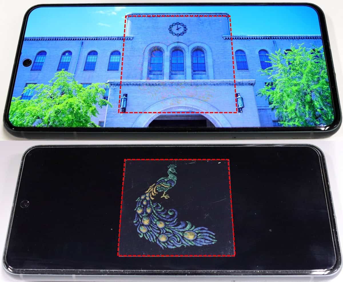
The majority of printing processes today are performed using different coloured pigments. However, there’s another type of colour called structural colour, which typically uses nanoscale structures that interact with light to produce a colour. By refracting and reflecting light at specific wavelengths, these nanostructures can produce incredibly bright colours that (unlike pigments) do not fade over time, unless the structure is physically altered. Structural colour is often found in nature – creating the brilliant colours of a peacock’s tail feathers, for example – but has been difficult to print using conventional printers.
Most instances of creating structural colour involve diffracting light through periodic polymers or transparent oxide nanostructures, but these approaches cause a strong iridescence – where the colour changes depending upon the viewing angle – which can limit the practicality for some applications. To print structural colour materials, other options are needed.
Researchers from Kobe University in Japan have now achieved this, by developing a Mie-resonant silicon nanoparticle ink that can be printed onto flat or three-dimensional surfaces using an inkjet printer. Mie resonant systems are highly refractive particle systems that enhance light–matter interactions at specific wavelengths and can boost optical effects.
“We undertook this research to bridge fundamental Mie-resonant nanophotonics with scalable printing technologies, enabling structural colour to move from laboratory demonstrations to practical, large-area applications,” explains Hiroshi Sugimoto, one of the study’s lead authors.
The research team at Kobe University has been developing spherical crystalline silicon nanoparticles with a high refractive index and low extinction coefficient that reflect specific wavelengths of light to produce certain colours. These particles, ranging in diameter from 100–200 nm, were used as the basis for the new ink, moving away from more traditional, unprintable structural colour materials.
The researchers wanted to develop structural colour inks that can be processed like conventional inks or paints. However, they initially found that when the solvent dried, the particles tended to aggregate. This aggregation changed how the particles interact with light and degraded the colouration of the ink. To overcome this issue, the team coated the silicon nanoparticles with thick silica shells and formulated them into a water-based acrylic emulsion. Unlike the crystalline silicon particles, the protective shells have a low refractive index so they don’t they don’t bend the light. As such, they provide a transparent coating that prevents aggregation without affecting the structural colour output.
The researchers used the nanoparticle ink to print images on a flat polymer film and a 3D metallic surface, using an inkjet printer at resolutions of between 250 and 125 dots per inch. They found that the images exhibited optical asymmetry – showing a different colour when light passes through the image (transmission) to when it is reflected from above – due to the Mie refraction that the particles exhibit.
The researchers also found that that the hue can be tuned by changing the diameter of the nanoparticles. This allowed them to create multi-colour patterns with tuneable reflection/transmission colour asymmetry by using nanoparticle inks with different particle sizes.
“The most important finding is that we achieved structural colour printing using silicon nanoparticles, overcoming the long-standing reliance on periodic arrays in conventional structural colour systems,” says Sugimoto.
Potential applications of these tuneable and printable inks include anti-counterfeiting images, semi-transparent smart windows, smart displays and vibrant art pieces (that won’t fade over time). For example, when the ink is printed on to a monitor, the printed images will be invisible when the display is on. However, when the display is turned off, the images become visible, which allows for information display without using any energy.
When asked about where they plan to take the research next, Sugimoto tells Physics World that “building on this work, we aim to further control and exploit this optical asymmetry for multifunctional systems, such as anti-counterfeiting and decorative films on buildings and windows, using scalable nanophotonic printing”.
The research was published in Advanced Materials.
The post Researchers print structural colour with an inkjet printer appeared first on Physics World.
Gwenaëlle Lefeuvre studied physics at Sorbonne Université in Paris, France, before moving to Université Paris Cité to do a PhD in experimental particle physics. After postdocs at Syracuse University in the US and the University of Sussex in the UK, she left academia and worked for 10 years at the UK company Micron Semiconductor Ltd. Here, Lefeuvre set up a business unit dedicated to designing and manufacturing CVD diamond sensors.
Lefeuvre now works as the network coordinator for Photonics Bretagne – a non-profit association in Brittany, France. As an innovation hub, the organization supports the development of the photonics ecosystem across industry, research and education in Brittany, and helps integrate photonics technologies into other sectors.
When it comes to skills I need for my role, my scientific background is just the starting point. I am the contact point between the Photonics Bretagne team, our members, our European partners, and any other parties interested in what photonics have to offer. While my background gives me credibility, what I really use is the inquisitive spirit that a physics education imprints in us. I ask a lot of questions, all the time and to everyone, so I can better understand what people work on, what they need, and how their products can be used in different situations.
Of course, this means that communication and networking are also crucial. Representing my member companies, for example, means that I must be able to translate what they are offering so it’s understandable for people who might work in a very different sector, such as mobility, agriculture or cosmetics.
Finally, being flexible is a must. I wear different hats depending on the task at hand, and need to be able to switch them around quickly.
I love many aspects of my role, but top of the list is having the opportunity to keep learning about new technologies and applications. The breadth and depth of knowledge my co-workers and our members possess is as humbling as it is inspiring. While I am more of a “generalist physicist” myself, I have worked on many different types of experimental systems so can appreciate the expertise at play.
I also enjoy the diversity of my work, which makes my days fun and varied. I might be meeting with members and looking for ways to support them; organizing a delegation visit with my European partners; or advocating for photonics in cross-sector events – and that’s just naming a few of my responsibilities. There is never a dull day.
With the diversity of my role and my enthusiasm to find out more comes the challenge of prioritizing. There are so many things I would love to be doing, but we are a small team and we must focus our efforts on those actions that can best serve our community. And of course, the administrative and reporting tasks are never loved by anyone and take up more valuable time than I would like. They are a constant in every job though, and can be managed through good planning.
Three things come to mind. The first is that it’s helpful to know whether you will enjoy becoming a highly specialized researcher, or if you would thrive in a more general role. Higher education in physics is designed around gaining a finer and finer degree of specialization. I realized during my postdocs that I was not enjoying staying in one given field (neutrino physics, in my case) as much as I expected to. What I loved was working hands-on with different types of sensors, which is a more transversal specialization, so to speak. Not everyone is built to be a specialist and there is nothing wrong with that. Many career options are open to those who embrace remaining curious about everything, provided they have a strong background to back it up.
There are so many ways to work in, with or for the physics community – the main limiting factor for my younger self was probably my own imagination
Secondly, it’s worth remembering that people change, and ambitions do too. It has been said many times in this column, but life isn’t linear and neither is a career. It is important to account for the person you will become, so that you don’t make choices today that will make your future self unhappy or stuck. There are so many ways to work in, with or for the physics community – the main limiting factor for my younger self was probably my own imagination. Luckily, many degrees now include broadening experiences like semesters abroad or entrepreneurship classes.
Finally, I wish I had realized earlier that people love it when we ask them questions about their work. Doing so does not showcase our ignorance but our interest – it’s a true win-win.
The post Ask me anything: Gwenaëlle Lefeuvre ‘Not everyone is built to be a specialist and there is nothing wrong with that’ appeared first on Physics World.
By harnessing the unique properties of tantala (tantalum pentoxide), a team of US-based researchers has created a photonic integrated circuit that can be tuned to deliver laser light across a broad spectrum of visible and infrared wavelengths.
The work was done by researchers at the National Institute of Standards and Technology (NIST) and colleagues at Octave Photonics.
From consumer electronics to atom-based metrology systems, many modern technologies depend on sources that deliver light at specific wavelengths. However, delivering high-quality narrow-band light is difficult – especially at visible wavelengths. As a result many of these technologies cannot be miniaturized to create low-cost, portable devices. Instead they must be implemented in bulky tabletop setups that are operated in expensive laboratory settings.
“Photonics technology offers routes to miniaturize components like laser sources and switches to the chip scale – devices smaller than a grain of rice,” explains study leader Grant Brodnik . “Different photonic materials have different strengths and limitations, and there is currently no single material ecosystem that can accommodate all the diverse demands of photonics.”
One promising solution involves integrating multiple advanced materials into the same device, harnessing combinations of their photonic properties to engineer capabilities that would not be possible with any single material. The key challenge is that many photonic materials have mismatched thermal, mechanical, and chemical properties, making them broadly incompatible with one another. So far, this has prevented researchers from seamlessly combining multiple materials into chip-scale devices.
To address this challenge, Brodnik’s team looked to the unique properties of tantala. A key feature of the material is that it can transform laser light at one frequency into laser light within a broad spectrum of light at visible and infrared wavelengths.
Tantala can be deposited onto other materials at room temperature, before being annealed at relatively modest temperatures of around 500 °C. In comparison, more conventional materials such as silicon nitride require annealing temperatures approaching 1200 °C.
Once deposited, tantala benefits from low internal mechanical stress, at around 38 MPa compared with around 800 MPa for silicon nitride. Together, these properties make it compatible with a broad range of underlying substrates and structures without damaging devices during fabrication.
In this latest work, Brodnik and colleagues deposited tantala directly onto a patterned thin-film substrate of lithium niobate – which itself an advanced photonic material. The result is a monolithically integrated, 3D photonic platform.
“We essentially sprinkle tantala directly on top of existing photonic circuitry,” Brodnik explains. “Then, we can make new photonics circuits on top, link other circuits below, or even operate together with the underlayer material and devices for new functionality.”
The team then showed that their combined platform is capable of a range of useful capabilities. “We demonstrated various photonic functions that involve generating new, custom-colour light sources from single-colour input lasers,” Brodnik says. “We also made frequency combs and supercontinuum, which are important tools for things like optical communications, precision metrology, and sensing applications.”
Several of these devices relied on the tantala and lithium niobate layers working in tandem. For instance, they used tantala to generate intense laser pulses, before passing light into the lithium niobate layer for further nonlinear processing. This allowed them to precisely measure the frequency of the laser light.
The work points to a new and broadly applicable route to the 3D integration of photonic materials, which could make it far easier to link advanced photonic functions across existing platforms.
In turn, this could open new pathways towards the scalable, affordable fabrication of complex photonic circuits, applicable in real-world devices. “New configurations offer opportunities to realise entirely new photonic designs that will drive lab experiments to field-deployable systems,” Brodnik says.
The research is described in Nature.
The post Tantala 3D integrated circuits deliver a rainbow of laser light appeared first on Physics World.
A laser plasma accelerator (LPA) has been used to power a free electron laser (FEL) for more than eight hours, delivering stable pulses of coherent light. The system was created in the US by researchers at the company Tau Systems and Lawrence Berkeley National Laboratory. The team says that its achievement represents a major breakthrough in stability for LPA-driven FELs, which could someday make coherent UV and X-ray pulses more accessible to academia and industry.
An FEL creates bright pulses of coherent light – usually in the ultraviolet-to-X-ray portion of the electromagnetic spectrum. These pulses are used in a wide range of research including physics, chemistry, biology and materials science.
The pulses are created by sending bunches of high-energy electrons through a device called an undulator, which applies a transverse magnetic field that alternates in direction as the bunch propagates. As the electrons are accelerated back and forth by the field they emit light. Under the right conditions the emitted light interacts with the electron bunch in such a way that the coherence and brightness of the light increases as the electron bunch travels through the undulator.
FELs require a bright and stable source of high-energy electron bunches, so today’s facilities are driven by large and expensive electron accelerators. The European X-ray Free Electron Laser, for example, is located at the end of a 3.4 km linear accelerator.
High-energy electron bunches can also be created by firing high-intensity laser pulses at a plasma target. Electrons in the plasma are much lighter than the ions, so they are accelerated more by the intense electric field of the laser pulse. The result is a region of separated positive and negative charge that contains a large electric field. This region trails the laser pulse like the wake of a ship – and is called a wakefield. If electrons are injected into this wakefield, they are captured and accelerated to near the speed of light. The process is similar to how a surfer is propelled by an ocean wave.
While LPA-driven FELs would require expensive lasers, their size and cost would dwarf that of accelerator-driven facilities. Today, however, the electron pulses delivered by LPAs are not good enough to drive a FEL. Some shortcomings are related to fluctuations in the focal point of the laser and well as changes in the pulse energy and duration. These fluctuations can be caused by mechanical vibrations, temperature fluctuations and other environmental disturbances.
Founded in 2021, the Texas-based company Tau Systems is developing practical LPAs for a range of applications including FELs. Now, the company has joined forces with researchers at Berkeley Lab’s BELLA Center to implement a set of laser-stabilization technologies on BELLA’s Hundred Terawatt Undulator beamline.
The team implemented five active systems that worked together to stabilize the focal point of the powerful laser. Some of this was done using a “ghost” beam – a low-power copy of the driving beam – to observe subtle fluctuations that would not be apparent by monitoring the main beam.
As a result the system delivered bunches of 100 MeV electrons at a frequency of 1 Hz and at high stability for over 10 h. These bunches were then used to drive a self-amplified spontaneous emission (SASE) FEL based on a 4 m-long undulator that is embedded within a vacuum chamber.
The LPA–FEL delivered violet (420 nm wavelength) pulses for more than 8 h without any human intervention. The FEL gain of the system was about 1000, which is the ratio of brightness of the emitted coherent FEL pulse to the brightness of light emitted by unamplified undulation.
This run is a significant improvement on the team’s 2025 achievement of using a LPA–FEL setup to deliver pulses of similar quality for an hour.
“This is the moment the community has been working toward,” says Stephen Milton of Tau Systems. “We have shown that an LPA-driven FEL is not just a proof-of-concept experiment. It is a platform capable of delivering the stability that real scientific and industrial users demand.”
Finn Kohrell of the BELLA Center adds, “Maintaining FEL stability for a record eight hours represents a significant advancement in LPA-driven FELs and provides deeper insights both into achieving optimal FEL performance and into validating LPAs as high-brightness injectors, which is crucial for LPA application in future light source facilities”.
During operation, the team gathered data about the stabilization process and mapped correlations between the parameters of the drive laser; the plasma source; the electron bunches; and the FEL’s output pulses. The researchers are now using this information to improve their control systems and they say that these data indicate that further gains in stability and brightness are possible.
The next experimental step will involve increasing the FEL energy to their system’s maximum value of 500 MeV.
“At this level, we can lower the undulator radiation wavelength to the 20–30 nm range, placing it in the hard ultraviolet or soft X-ray regime,” explains Kohrell. “[This would be] a crucial step toward making the technology viable for real-world applications.”
The new system is described in Physical Review Accelerators and Beams.
The post Laser-driven free electron laser runs for more than eight hours appeared first on Physics World.