
❌

Normal view

‘Kinetic electronics’ make self-connecting circuits
14 August 2026 at 09:00
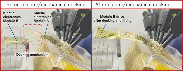
Side-by-side photos showing a pair of circuits before and after they connect
Come together: Kinetic electronics module A, which integrates an electrical circuit and an actuator, deforms in response to an electrical input and connects mechanically and electrically to thin-film circuit module B via the docking mechanism. Before connection (left image), the two modules are separate; after connection (right image), module A holds and lifts module B, and by supplying power through the connection point, it can independently drive module B to deform. (Courtesy: Fumihiro Sassa/Kyushu University)

Researchers at Kyushu University in Japan have developed a flexible electronic circuit that can connect itself to another electronic circuit and then disconnect from it. The prototype structure is an important step towards electronic devices that can reconfigure and even repair themselves, and it could have applications in wearable sensors, soft robotics and medical devices.

Most of today’s electronic devices are fixed, or “non-modular”, explains study leader Fumihiro Sassa of Kyushu University’s Department of Electrical and Electronic Engineering. Typically designed for specific tasks or environments, they are not readily adaptable to new ones, and they often cease to function if even a single component in their electronic circuitry fails. This leaves them dependent on human operators or external robotic systems if it becomes necessary to expand their functionality or repair damage.

“This can be a serious limitation inside very small machines, in space equipment, in devices requiring specialized handling, such as wearable chemical sensors, or in systems containing very large numbers of wires and electronic elements,” Sassa explains. “In such cases, in-situ repair can be difficult. The whole system may need to be replaced.”

Connection and disconnection

To overcome this problem, the Kyushu University researchers have been developing what they term “kinetic electronics” modules. These consist of electronic circuits and actuators that deform when an electrical current is applied to them so that they can mechanically and electrically connect to other modules. Before this connection takes place, different modules are separate, but after connection or “docking” takes place, one module can independently deform another when power is supplied through the point that connects them.

In this way, explains Sassa, the circuits can rearrange their own hardware structure. “Such functions have traditionally been used in mechanical systems, such as spacecraft, trains and modular robots, but we have now applied them to an electronic device.”

Sassa and colleagues fabricated their electrothermal bimorph actuators from polypropylene and polyimide films with heater electrodes and electrical circuits formed on them through a two-dimensional top-down process. Because the two polymers expand differently, Sassa explains that Joule heating causes selected actuator sections to bend. “Prescribed sequences of these motions produce docking and undocking and once docked, passive mechanical engagement maintains the connection without continuous power being supplied,” he says. “Undocking requires a separate actuation sequence.”

Towards miniaturization and more intelligent control

The researchers say they are working on miniaturizing their system and looking how to control it more intelligently. In the present study, which is detailed in npj Flexible Electronics, they demonstrated the docking mechanism using a small number of millimetre-scale independent sensors and actuators formed together on the circuit, with motion being controlled in sequence by an external microcontroller. They are now developing photolithographic processes to further decrease the size of these components and have already fabricated actuators smaller than 100 μm using these techniques.

“In a similar way to large-scale integration in conventional electronics, doing this will allow us to integrate very large numbers of these sensing and actuation elements, allowing the electronic circuit to form and change much more complex mechanical structures and functions,” says Sassa.

“We are also interested in so-called distributed control, in which the central controller does not need to specify every movement,” he adds. “Instead, many elements would follow relatively simple local control rules, from which advanced self-reconfiguration and self-organization could emerge.”

The post ‘Kinetic electronics’ make self-connecting circuits appeared first on Physics World.
Machine vision begins to work like the human eye

8 July 2026 at 09:15

Artificial vision is employed in applications ranging from self-driving cars to advanced robotics. However, most “artificial eyes” do not work well in complex real-world conditions, such as sudden strong glare, dimness or uneven light levels. Such devices also rely on complex and rigid electronic circuitry to adjust their sensitivity to light and on post-algorithmic processing for accurate image recognition. A research team headed up at the University of Electronic Science and Technology of China and Penn State in the US has now developed a new adaptive photomemristor structure that does not suffer from any of these problems, allowing for machine vision that truly adapts to natural and complex light fluctuations, just like human eyes.

Sight is one of our most important senses: we acquire over 80% of the information from our environment through our eyes. Indeed, the human eye is so sensitive that it can process visual information under varied lighting levels with a photodetection dynamic range of more than 160 dB. This allows us to watch a film in a dark room or drive in the glare of oncoming headlights. Until now, however, artificial eyes have lacked this so-called dynamic self-adaptation.

Memristors for improving light adaptation

In recent years, researchers have been looking into neuromorphic devices that mimic the way biological structures work. These devices can be engineered to behave very much like neurons in the human brain, which learn by reconfiguring the strengths of the connections (synapses) between neurons. Memristors (or memory resistors) are excellent in this respect because they can bring this learning functionality to the connections in electronic circuits.

Rather than being fixed, the resistance of memristors changes depending on the current or voltage previously applied to them. This means that specific resistances can be programmed into the devices and subsequently stored. Importantly, the “remembered” value of the resistive state persists even when the power is switched off, making it a non-volatile form of electronic memory.

Photomemristors are a type of memristor that can change their resistance in response to both voltage/current and light and could therefore be used in advanced optical systems.

Reversible water absorption and desorption

In the new work, reported in Nature Communications, a team led by materials scientist Jia Zhu made a highly adaptive optoelectronic synapse from the composite material TiO₂/PEDOT:PSS. The TiO2 absorbs light, converting it into a photocurrent that then passes through the conductive surface of the PEDOT:PSS polymer. This intrinsic photothermal effect, explains Zhu, triggers reversible water absorption and desorption on the polymer surface, which in turn impacts the device’s conductivity.

“This process allows the device to automatically suppress the photoresponse under intense bright light and amplify its sensitivity under dim weak light,” he says. “In extreme strong-light conditions, its photocurrent can even drop below the dark current level, allowing for an ultralow-sensitivity state similar to human eye pupil constriction.”

A high image recognition accuracy

Zhu tells Physics World that when integrated with artificial neural networks, the new adaptive vision system achieves a high image recognition accuracy of 91.3% in dynamically changing mixed-light scenarios, including glare, dim shadow and alternating brightness. It also eliminates the need for bulky auxiliary circuits and complex real-time computing algorithms,  reducing power consumption and hardware volume.

The new work is a first step towards making next-generation neuromorphic vision systems that could be used in practical applications. “Our adaptive photomemristor vision system can effectively resist strong glare from oncoming vehicle headlights, accurately identify pedestrians, lane lines and traffic signals in complex day–night alternating light environments, so greatly improving the safety of autonomous driving,” Zhu explains.

The technology could also be widely applied to humanoid robots, outdoor intelligent monitoring equipment, aerial reconnaissance and portable intelligent vision terminals, he adds.

Looking ahead, the researchers will now focus on optimizing the material formula of the compound studied in this work and improve its fabrication. They will also be working on complete system-level integration, including array device packaging, signal readout modules and adaptive control units, with the aim of constructing a fully functional bionic artificial eye prototype. “We will then verify whether this biomimetic dynamic regulation strategy can be extended to other oxide/polymer composite memristor systems to develop a universal design principle for high-performance light-adaptive neuromorphic devices,” says Zhu.

The post Machine vision begins to work like the human eye appeared first on Physics World.

New superconducting diode gives greater control over the flow of electrons

2 July 2026 at 15:00

Like a two-lane highway with one lane empty and the other clogged with traffic, superconducting diodes allow electrons to flow without resistance in one direction while encountering normal, resistive conditions in the other. First demonstrated experimentally in 2020, these devices have considerable potential as platforms for fundamental studies of quantum materials and as building blocks for superconducting electronics.

For many applications, being able to control the flow of electricity through the diode – or even reverse its polarity – is essential. In principle, there are several ways of doing this because the efficiency of the superconducting diode effect (SDE) depends on many factors. Examples include magnetic field, temperature and diode design as well as intrinsic properties such as the momentum of the Cooper-paired superconducting electrons and their spin-orbit coupling.

In practice, though, some of these properties are more easily changed than others. To return to the highway analogy, it’s much more straightforward to alter the flow of traffic by posting new road signs, rather than by rebuilding the road or redesigning the cars.

In a recent paper in Chinese Physics Letters, Yanwu Xie, Yishuai Wang, Wenze Pan and Meng Zhang of Zhejiang University in Hangzhou, China describe a new superconducting diode platform that makes it far easier to change the device’s configuration, and thus to control the flow of superconducting electrons through it. Physics World spoke to them about their research and its possible applications.

How did you get the idea for this new type of superconducting diode?

This work started with an unexpected experimental observation. While we were making routine current-voltage measurements on a conventional strip-shaped superconducting device constructed at the interface between two materials, LaAlO3 and KTaO3 (LAO/KTO), we noticed a pronounced difference between the critical currents in opposite directions. Given the growing interest in the SDE, this surprising result immediately caught our attention and prompted us to investigate its origin.

What is special about these two materials?

The properties of conventional superconducting diodes are typically locked into their fixed physical structures, such as Josephson junctions or patterned vortex pinning sites. This inflexibility makes post-fabrication tuning or reconfiguration of the diode characteristics extremely challenging.

Two-dimensional oxide interface superconductors such as LAO/KTO and LaAlO3/SrTiO3 are good candidates for overcoming this problem. The strong spin-orbit coupling near the interface enables possible finite-momentum Cooper pairing, while the extremely low superfluid density and intrinsic two-dimensional nature of the materials create ideal conditions for studying vortex dynamics and magnetic flux behaviour.

In addition, these systems have exceptional tuneability. Their superconducting states can be well controlled through both global substrate gating and local conductive atomic force microscope (cAFM) lithography, which opens new possibilities for post-fabrication SDE engineering.

What was the most challenging aspect of this research?

The most challenging part was unravelling the frustrating sample-to-sample variability we encountered early on. We now know that the SDE in conventional LAO/KTO devices stems from asymmetric vortex entry conditions caused by random, fabrication-induced edge imperfections. At the time, however, even devices with nominally identical geometries exhibited wildly different SDE efficiencies and polarities, showing no discernible systematic trend.

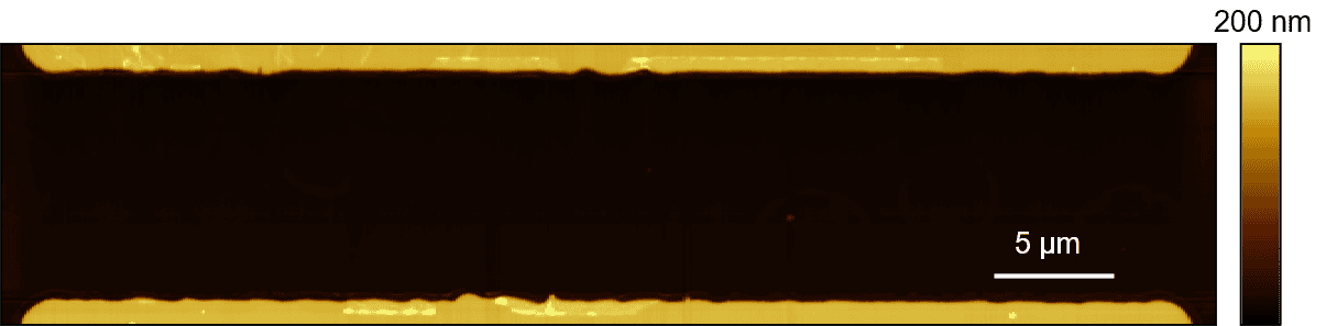
The breakthrough came when AFM imaging revealed random edge defects on the superconducting channels. To test whether these random imperfections were indeed the root cause, we used cAFM lithography to “straighten” the originally photolithography-produced rough channel boundaries. This atomic-scale trimming strongly suppressed the SDE, providing unambiguous evidence for the vortex edge asymmetry mechanism.

AFM image showing two horizontal yellow-orange surfaces separated by a larger black gap. The inner edges of the surfaces are visibly bumpy.
Channel edges: An atomic force microscopy (AFM) image of the LAO/KTO channel in the diode, showing the roughened edges. (Courtesy: Yanwu Xie)

We then turned this challenge into an opportunity. By using cAFM to re-shape the channel edges repeatedly and in a non-volatile way, we transformed a source of random sample variability into a tool for deterministic, on-demand quantum device control.

What are some possible applications for this editable superconducting diode?

The nonreciprocal transport of charge carriers – exemplified by p-n junctions in semiconductor diodes – is a cornerstone of modern electronics. Similarly, superconducting diodes are emerging as pivotal components for superconducting electronics. What distinguishes our approach is our ability to reversibly modify the diode polarity and efficiency within the same device through nanoscale control of the superconducting channel geometry. This editability may enable reconfigurable superconducting circuit elements and adaptive circuit architectures, while also providing a versatile platform for investigating the role of geometry-associated vortex dynamics in nonreciprocal superconducting transport.

What will you do next?

We plan to fully exploit the unique cAFM lithography capability of our oxide interface platform to systematically investigate how tailored vortex-boundary configurations shape the SDE. The diode performance can be further optimized by mapping out the precise relationship between channel geometry, vortex entry barriers and rectification efficiency.

In parallel, we plan to introduce artificial pinning centres (such as nanoscale insulating dot arrays) directly into the superconducting channel. This will allow us to engineer asymmetric vortex-pinning landscapes within the bulk of the channel. Combining this engineered flux pinning with the asymmetric vortex-boundary mechanism demonstrated in the current work offers a promising route toward achieving a robust, deterministic and highly controllable superconducting diode.

The post New superconducting diode gives greater control over the flow of electrons appeared first on Physics World.

❌