Coway employees and Gyeongil Elementary School students plant vegetation in the third Coway Ecological Forest. (Photo: Coway)
Coway employees and Gyeongil Elementary School students plant vegetation in the third Coway Ecological Forest. (Photo: Coway)
Coway has created an ecological forest featuring endangered and rare plants at Gyeongil Elementary School in Seongdong District, Seoul. The site will serve as an ecological learning space where students can observe plants and other living organisms.
Coway said on Sept. 16 that it created the third Coway Ecological Forest, covering about 365 square meters, on the school's grounds.
Coway planted 1,195 plants from 25 species, including endangered and nationally protected species such as Pseudolysimachion pusanensis, Hosta yingeri and Aster koraiensis. Coway employee volunteers and Gyeongil Elementary School students participated in the planting.
Environmental social enterprise Tree Planet and the Landscape Architecture Design Lab at the University of Seoul were responsible for the forest's design and construction. The ecological forest incorporates results from research collaboration between the two organizations.
Environmental education for students was also conducted after the forest was completed. Students observed the forest and completed ecological forest checklists. Coway selected 13 students as ecological forest gardeners and provided them with garden maintenance kits.
Coway operates an ecological forest program that plants endangered and rare species in South Korea designated by the International Union for Conservation of Nature (IUCN) and the Korea Forest Service, as well as plants endemic to the Korean Peninsula. The company created its first ecological forest in an outdoor space at its headquarters in 2024 and its second at Banghwa Elementary School in Seoul last year.
Coway also operates environmental social contribution programs including Clean School Classroom Forest, which provides air-purifying plants to elementary schools; river plogging to collect waste along waterways; and the throwing of effective microorganism (EM) mud balls to improve water quality.
Novathermo CEO Kim Hyung-chul. (Photo: Novathermo)
Novathermo CEO Kim Hyung-chul. (Photo: Novathermo)
Novathermo, a thermal management materials startup, is focusing its resources on thermal materials for artificial intelligence (AI) semiconductors and automotive electronics. Following the commercialization of a high-thermal-conductivity material for printed circuit boards (PCBs), the company has added silicone thermal pads to its product lineup. It aims to reach 36 billion won in sales by 2030.
Kim Hyung-chul, CEO of Novathermo, said on Sept. 16 that PCB thermal materials require significant time for final validation because they undergo multiple processes while still in a semi-finished state, while thermal interface material (TIM) silicone pads can be evaluated by customers in a form close to the finished product after production and before shipment.
"It is significant because this is our first commercial product line that expands our thermal management technology into the TIM market, where demand is substantial," Kim said.
Novathermo develops and produces new polymer-based thermal materials using carbon nanotubes (CNTs). Its main products are designed to rapidly transfer heat generated by semiconductors and automotive electronic components while maintaining electrical insulation. The company is developing thermal materials for PCBs, semiconductor packaging and power electronics.
Its core technology involves uniformly dispersing highly thermally conductive materials such as CNTs and alumina within polymers. Novathermo uses a high-shear mixing process to reduce material agglomeration and create pathways for heat transfer. The technology is designed to improve thermal performance while maintaining electrical insulation and mechanical strength.
Its flagship product is Aqua, a high-thermal-conductivity material for PCBs. PCBs are substrates that connect semiconductors and other electronic components. Aqua enables the PCB material itself to conduct heat efficiently, allowing heat generated by chips to dissipate through the substrate as well.
Heat generated by semiconductors is typically removed through heat sinks or cooling systems positioned above the chip. Aqua adds another heat-transfer path through the underside of the substrate. In Novathermo's own tests, replacing only the material with Aqua while keeping the substrate thickness and component configuration unchanged reduced chip temperatures by as much as 30% and substrate temperatures by 20%. The product was commercialized in November last year.
The material achieves thermal conductivity of about 2 watts per meter-kelvin (W/m·K) on mass-production equipment. Novathermo has achieved up to 3.3 W/m·K at the laboratory stage. Thermal conductivity measures how effectively a material transfers heat, with higher values indicating faster heat transfer.
Novathermo has also completed customer validation for automotive components. In a comparison of identical circuits using different PCB materials in an automotive lidar module, Aqua lowered the temperature of the transmitter (Tx) chip by more than 10 degrees Celsius compared with the conventional material. The company said that exceeded the customer's initial target of a 4-degree reduction.
The company is also conducting proof-of-concept (PoC) projects with global companies. PoC involves applying the material directly to a customer's product to determine whether it meets required performance specifications. Successful validation could lead to additional reliability testing and discussions on mass-production supply.
Novathermo has also introduced FLEXURE, a silicone thermal pad brand. It has established mass-production capabilities for products with thermal conductivity ratings of 3, 5 and 8 W/m·K. The company has also completed prototype design for a high-performance 12 W/m·K product line.
FLEXURE is placed between a semiconductor chip and a heat sink. Microscopic gaps form between the surfaces of the chip and heat sink, and air trapped in those spaces can impede heat transfer. The silicone pad fills the gaps, transferring heat generated by the chip to the heat sink.
A key challenge in product development is achieving both thermal performance and suitable physical properties. Adding more filler to increase thermal conductivity can make a pad harder or more prone to tearing while reducing its ability to conform to component surfaces. Novathermo adjusted the filler composition, silicone structure, cross-linking and molding processes to improve thermal conductivity, dimensional stability and surface conformity.
Novathermo plans to expand its customer base in semiconductor packaging, power electronics and automotive electronics, centered on its high-thermal-conductivity PCB materials and silicone TIM pads. Its current mass-production yield is about 70%.
The company also plans to expand production capacity. Monthly output is targeted to rise from 10,000 panels this year to 1.2 million panels in 2030. Over the same period, the number of key customers is expected to increase from three to 25, while exports are targeted to rise from 10% to 55% of sales. Novathermo aims for 36 billion won in revenue by 2030.
"Customers requesting samples are focusing not only on thermal performance but also on the pads' ability to resist tearing and maintain surface conformity even under high-hardness conditions," Kim said. "We will improve product quality and mass-production reliability to help localize high-performance thermal materials that are heavily dependent on overseas suppliers and stabilize the supply chain."
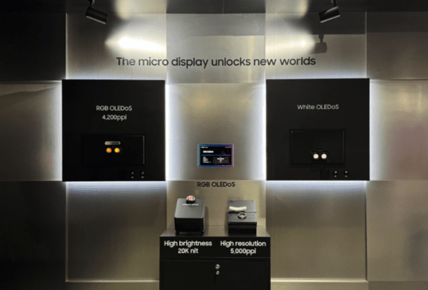
An OLEDoS product displayed by Samsung Display at AWE USA 2025. (Photo: Samsung Display)
An OLEDoS product displayed by Samsung Display at AWE USA 2025. (Photo: Samsung Display)
Samsung Display plans to invest about 300 billion won to mass-produce red, green and blue (RGB) OLED-on-Silicon (OLEDoS) displays. Sunic System will supply the deposition equipment, which accounts for about half of the investment.
According to industry sources on Sept. 15, Samsung Display will hold an investment review committee meeting this month to finalize investment in 12-inch RGB OLEDoS mass production. The line will have capacity to process 3,000 wafers per month, with the investment estimated by the industry at about 300 billion won. The location has not been confirmed, but the line is likely to be built at the A2 plant, which already has a 12-inch white OLEDoS (WOLEDoS) line.
Samsung Display evaluated 12-inch RGB OLEDoS deposition systems from Sunic System and Japan’s Canon Tokki earlier this year. After comparing equipment performance and supply experience, the company selected Sunic System.
The deposition equipment to be supplied by Sunic System is expected to cost about 150 billion won, roughly three times the 40 billion won to 50 billion won price of conventional OLEDoS deposition equipment. The higher cost reflects the need for significantly tighter vibration control and mask-to-wafer alignment precision to form RGB emissive layers on individual subpixels.
The remainder of the capital expenditure will go toward front- and back-end equipment for encapsulation, inspection, cleaning and material handling. Actual spending may vary depending on equipment specifications and the extent to which existing infrastructure can be used.
Equipment orders are expected in the fourth quarter. Following approval of the investment, Samsung Display is expected to finalize detailed equipment specifications, delivery schedules and acceptance conditions before signing purchase contracts.
Samsung Display is considering bringing in equipment in 2027 and starting mass production of RGB OLEDoS in 2028. Equipment manufacturing, installation, commissioning and process stabilization are expected to take more than a year.
OLEDoS is a microdisplay that forms OLED emissive layers on a silicon wafer. It is divided into white OLEDoS and RGB OLEDoS depending on how colors are produced.
WOLEDoS uses color filters over a white organic light-emitting diode (OLED) emissive layer to produce RGB colors. Because organic materials do not need to be separately deposited for each subpixel, the deposition process and mask-alignment requirements are less demanding. Mass-production technology and supply chains are already established, and WOLEDoS is used in commercial extended reality (XR) devices including Apple Vision Pro.
Some light, however, is lost as white light passes through the color filters. Increasing screen brightness requires more power, which can result in disadvantages in heat generation and battery life.
RGB OLEDoS directly deposits red, green and blue emissive layers on individual subpixels. Eliminating color filters reduces light loss and offers advantages in brightness, luminous efficiency and color reproduction.
RGB emissive layers can be formed using either mask-based or maskless methods. Samsung Display is expected to use a mask-based deposition process. Forming emissive layers on subpixels measuring only a few micrometers requires repeated, highly precise alignment of the mask and wafer during deposition.
A tandem structure requires multiple emissive layers to be stacked, increasing the number of deposition chambers and transfer systems. Controlling mask sagging, thermal deformation, positioning errors and deposition-thickness variations across an entire 12-inch wafer also presents technical challenges.
Samsung Display acquired US microdisplay company eMagin in 2023 and has since been developing RGB OLEDoS technology. The yield of eMagin’s 8-inch RGB OLEDoS process is known to be about 20%.
Expanding wafer size from 8 inches to 12 inches makes controlling deposition uniformity and alignment errors more difficult. Samsung Display’s actual mass-production schedule and output will depend on its ability to secure sufficient yields on the 12-inch process.
“RGB OLEDoS has advantages in brightness and efficiency, but mass production on 12-inch wafers has yet to be proven,” an industry official said. “How quickly yields can be stabilized after the equipment is installed will determine the timing of commercialization.”

 Login