❌

Reading view

At 0.8 nanometers, carbon film may replace two layers in future chip wiring

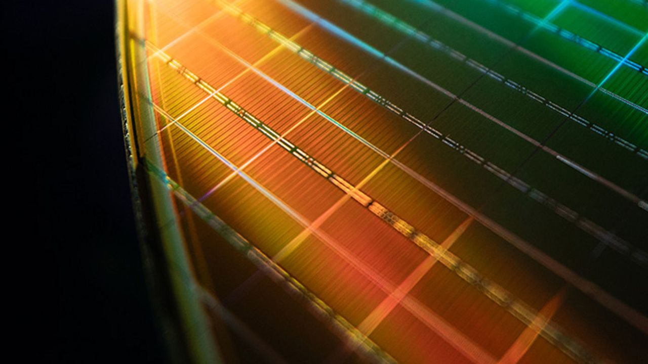
As transistors inside microchips continue to shrink, the metal wiring that connects them is becoming a growing obstacle to faster, more energy-efficient chips. Narrower wires have greater electrical resistance, while smaller gaps between them increase interference between adjacent signals. These effects impede data transfer and raise energy consumption—an issue known as an interconnect bottleneck, which is especially acute in data-hungry artificial intelligence processors.

  •  

Intel raises $19.7 billion to help fund future projects as 14A production looms — share sale attracted $100 billion in demand, report claims

Intel is set to raise $19.7 billion by selling new common stock in a bid to finance the building out of new production capacity, the development of next-generation leading-edge process technologies like 14A and others, and day-to-day operations. While the company does not assign money to a particular project, Intel needs to build capacity to land orders from large external clients, so capacity expansion will likely be a priority. According to Bloomberg, the share sale attracted $100 billion in demand.

Intel will sell 210,526,315 shares for $95 apiece through an underwritten public offering. In addition, participating banks have 30 days to acquire as many as 31,578,947 more shares at the same $95 price, minus applicable underwriting discounts. Should they exercise all their options, Intel could sell approximately 242.1 million shares altogether and increase the proceeds to roughly $23 billion. Without the additional shares, Intel expects net proceeds of approximately $19.7 billion after underwriting discounts, commissions, and estimated expenses. The transaction is scheduled to close on August 12, 2026.

Intel's market capitalization increased from roughly $90 billion last August to $491 billion at press time, so the time is right to sell some shares and raise some much-needed cash, as the company must compete against giants like TSMC and Samsung, which spend tens of billions of dollars every year on new fabs and advanced process technologies. Meanwhile, Intel's capitalization reached its all-time high of $673 billion on June 20, 2026.

Intel has not assigned the money it is going to raise to particular projects and says the capital can be used across the business, including for capital expenditures and working capital. The company is currently ramping up its Fab 52 in Arizona and is on track to start using adjacent Fab 62 when it needs to. In addition, the company still has to build its fab complex in Ohio, which is expected to cost over $100 billion when fully built, so it badly needs money.

In its risk disclosures, the company specifically mentioned Intel 14A — which is due to enter mass production in 2028 — and other advanced process technologies, manufacturing expansion required to support them, and the need to secure design wins and volume commitments from major external foundry customers. While Intel does caution that these long-term investments amounting to tens of billions may not generate adequate returns, it is impossible to land sizeable contracts from external customers without having production capacity readily available.

Interestingly, Intel also mentioned alternative financing arrangements, government grants, and the U.S. government's significant equity position in the company among relevant factors.

  •  

US lawmaker wants gov't to enforce regulation to ensure 'chipmakers conduct adequate due diligence on their customers' — House member calls for Biden-era export control to be enforced

House Select Committee on China Chairman John Moolenaar has written a letter that demands the U.S. government enforce an existing export control measure designed to prevent Chinese companies from getting advanced chips produced by contract chipmakers like TSMC or Samsung Foundry.

When Joe Biden was about to leave the office in early 2025, he signed a law that required chipmakers to determine their end customers in a bid to prevent contract manufacturers from unknowingly fabricating chips using American technologies for companies that served as intermediaries for restricted organizations tied to the Communist Party or the People Liberation Army. The regulation was introduced after it was discovered that chips made by TSMC for China-based Sophgo were actually Huawei's Ascend 910B AI accelerators. However, the Trump administration announced in May 2025 that it would not enforce this semiconductor regulation known as the 'Foundry Due Diligence Rule,' which naturally created uncertainty about whether the foundry-focused requirements would be actively implemented at all.

"The announcement created ambiguity as to whether front-end fabricators like TSMC can export unpackaged advanced dies to non-approved designers located outside of China, without performing the due diligence specified in the Foundry Due Diligence Interim Final Rule (IFR)," the letter reads. "These exports enabled Huawei to obtain millions of controlled Ascend logic dies from TSMC, using its front company, Sophgo in 2023 and 2024."

Before the adoption of the 'Foundry Due Diligence Rule,' Chinese companies and/or their intermediaries could misrepresent chip specifications and end users when placing orders with TSMC or other foundries, which allowed restricted devices to be made despite U.S. export controls. Under the rule, foundries and OSAT providers exporting chips produced on 14/16nm-class process technologies or more advanced nodes must presume those devices qualify as controlled AI processors subject to a global licensing requirement, unless they meet an exemption. According to the letter, foundries have generally complied with these requirements since the rule took effect. As a result, Moolenaar essentially asks the government to enforce the existing controls rather than introduce stricter export controls.

Moolenaar believes that the Commerce Department's Bureau of Industry and Security could clarify its current stance on the Foundry Due Diligence Rule in two ways:

  • By issuing guidance, which confirms that the worldwide Regional Stability (RS) licensing requirement still applies to exports from front-end foundries;
  • By formally annulling the AI Diffusion IFR and amending §744.23 to explicitly restore that requirement for both foundries and OSAT providers.

Either approach would eliminate conflicting interpretations and reinforce enforcement of existing export controls, Moolenaar believes.

  •  

Hyperscalers commit nearly $2 trillion to secure AI hardware and memory — Google leads $811 billion spending surge while Apple trails at $57 billion

Apple used to be among a few companies willing to buy memory and other components worth billions of dollars under long-term supply contracts at fixed prices. But the artificial intelligence era represents a new reality with new purchasing champions, marking a tectonic shift in the high-tech world. Alphabet, Microsoft, Meta, and Amazon have purchase commitments totaling about $2 trillion, and a significant portion of these commitments are for memory, according to estimates by analyst Claus Aasholm. While the commitments are approximate, span many years, and should be generally taken with a grain of salt, they still reflect the direction the industry is moving.

Combined purchasing commitments from the four major hyperscalers shown in the chart —Amazon, Alphabet, Meta, and Microsoft — reached nearly $2 trillion by Q2 2026, with Alphabet and Microsoft accounting for the overwhelming majority of the total.

The rapid expansion suggests several major findings. Firstly, the AI infrastructure race is accelerating, not stabilizing. Secondly, AI infrastructure investments are driven by a handful of hyperscale cloud service providers (CSPs) whose long-term procurement commitments now vastly exceed those of traditional consumer electronics companies such as Apple.

Thirdly, memory has become a strategic asset — perhaps a competition weapon — rather than a commodity. Fourthly, suppliers of memory — both 3D NAND and DRAM — are gaining pricing power. Finally, demand for memory will likely drive major capacity expansion at Micron, Samsung, and SK hynix, even though so far these companies have been exceptionally disciplined about their capacity investments.

Almost $2 trillion commitments

Google shows by far the most aggressive increase in purchasing commitments, rising from roughly $140 – $150 billion in Q3 2025 to around $811 billion by Q2 2026 (though these are total purchase commitments by Alphabet, not specifically memory purchase commitments), while Microsoft follows a similar trajectory and reaches approximately $678 billion in total obligations, which includes, but is not limited to memory.

Meta is also ramping commitments substantially to around $349.3 billion (again, these are total commitments), whereas Amazon increased its commitments more gradually to roughly $130 billion. By contrast, Apple — which makes the world's most popular smartphone, and which was the largest consumer of memory just a couple of years ago — remains almost flat throughout the period at approximately $57 billion (of which $56.2 billion is payable within 12 months). Apple's commitments fall well short of Nvidia's commitments of $119 billion.

Memory suppliers used to buzz around Apple like fruit flies, but now they have discovered larger commitments.Apple's purchasing commitments have not changed, suggesting a reluctance to follow the new market rules.https://t.co/0pRbk8aYVJ pic.twitter.com/t2VNm7uw1dAugust 6, 2026

Again, we are talking about total purchase commitments, which include foundry capacity, 3D NAND, and DRAM memory, but are not limited to them. Alphabet, Amazon, Meta, and Microsoft all build custom silicon and custom servers, so a significant portion of these commitments is to various EMS providers.

While $1.968 trillion of purchase commitments for memory and storage alone would be an absurdly large amount of money, a huge portion of these commitments consists of contract manufacturing obligations as well as memory chips. This suggests that the foundry, 3D NAND, and DRAM markets are entering a new phase in which hyperscalers are willing to make vastly larger forward purchasing commitments than traditional consumer-electronics companies, giving suppliers a strong incentive to prioritize customers prepared to secure future capacity on that scale.

Strategic assets

While Claus Aasholm's chart is explicitly dedicated to memory, it does describe total purchase commitments of tech giants, so the chart can reasonably be read as evidence that memory and capacity at TSMC, Samsung Foundry, and GlobalFoundries are becoming a strategic asset rather than merely another component to procure at the best available price.

AI infrastructure requires enormous quantities of AI accelerators, DRAM (including HBM), and 3D NAND. Meanwhile, the supply of high-end memory (HBM) is constrained by fab capacity at major DRAM makers, whereas the supply of AI accelerators is constrained by both wafer capacity and foundries and packaging capacity at foundries and their OSAT partners. As a result, hyperscaler CSPs have an incentive to lock in supply years ahead, even if doing so requires exceptionally large purchasing commitments.

That also changes the relationship between semiconductor suppliers and their customers. In theory, a company willing to guarantee hundreds of billions of dollars of future purchases can effectively help underwrite expansions of foundry, memory, and advanced packaging capacity and, in return, secure priority access to scarce products and future process technologies. In reality, TSMC can well afford capacity expansion using the money it gets from hyperscalers and give priority to its largest customers. In this environment, access to DDR5, HBM, and 3D NAND memory becomes part of the competitive advantage rather than merely a procurement exercise.

This is also what makes Apple's position in the graph interesting: its purchasing commitments barely move while those of Alphabet, Amazon, Meta, and Microsoft surge. If the trend continues, Apple may remain one of the world's largest semiconductor buyers in absolute terms, but the question is whether it will be among the key customers that foundries, memory makers, and OSATs plan their future capacity expansions.

An inflection point

Perhaps the most interesting takeaway of the findings revealed by long-term purchase commitments is that the industry's center of gravity appears to have shifted.

During the smartphone era, foundries (well, TSMC has won) and memory suppliers often competed aggressively for Apple's business because of its enormous purchasing power. Today, hyperscalers building AI infrastructure are making purchasing commitments that dwarf those of traditional CE companies like Apple, which may well represent a strategic inflection point akin to the one Andy Grove described in his 'Only the Paranoid Survive' book.

Will this tectonic shift result in prioritization of customers capable of enabling future capacity expansions through massive long-term purchase agreements, or will foundries and memory makers remain more or less disciplined with their capacity expansions so as not to lose a lot when demand declines? This is a question that has yet to be asked.

In any case, the AI megatrend has transformed semiconductors — from foundries to advanced packaging and from DDR5 to HBM4 — into strategic assets that can no longer be treated as ordinary components procured on demand. And this is something that will continue in the long run.

  •  

Musk’s Terafab projected to be larger than the Pentagon, Apple Park, Mall of America, and Giga Texas, combined — all-in-one chip manufacturing facility visualized to show the project’s massive footprint

Most megafactories usually take years to go from conceptualization to construction, but a recent drone flyover of the Terafab showed that progress has already started on the ground less than five months after Musk unveiled it. However, the video doesn’t do justice to the true scale of its footprint, so X user Nic Cruz Patane created a visualization to help us understand how large the chip manufacturing facility is.

Terafab approximate size comparison between Giga Texas, the Pentagon, Apple Park, and the Mall of America.There has never been a building this large. Elon Musk says it will be the most valuable building by far. pic.twitter.com/GCmpfeduJnAugust 6, 2026

The site will reportedly have a floor space of at least 100 million square feet, making it larger than Giga Texas (10 million sq. ft), the Pentagon (6.6 million sq. ft), Apple Park (2.82 million sq. ft), and the Mall of America (5.6 million sq. ft), combined. This also makes it significantly larger than New Century Global Center in Chengdu, China, with has an interior space of “just” 18.9 million sq. ft.

While this might seem like an absurd amount of space for chip manufacturing, it appears that the Terafab will need it because it’s going to be more than just a chip fab making AI processors — instead, it will be an all-in-one facility that will produce logic and memory chips, as well as have lithography, packaging, and testing under one roof.

Elon Musk started talking about building his own chip manufacturing facility in late 2025 and officially announced the project in March of this year. The reasoning behind this project is that both SpaceX and Tesla will require at least 1TW of compute, which is more than ten times that current global chip supply.

Nvidia CEO Jensen Huang warned that a project like this will be an “extremely hard” challenge, but it appears that Musk is willing to put his massive resources on the line for this. Intel CEO Lip-Bu Tan even said that he can “think of no better partner than Elon Musk” to explore “unconventional” ways of chip manufacturing.

Musk is no stranger to both leading and funding projects that otherwise seemed impossible. Although he did not found Tesla, his investment and leadership in the company led it to become an industry trailblazer in EVs. He fundamentally changed commercial space travel with SpaceX; something that used to be the purview of NASA and other national governments, and he also broke a record when he set up 100,000 Nvidia H200 GPUs in just 19 days back in 2024 — a process which Huang said usually takes four years.

It seems that Terafab is Musk’s biggest project to date, which is estimated to require up to $119 billion in investments. But even though it seems that this project already has a secure customer base in SpaceX and Tesla, the former acknowledges that there’s a risk that this ambitious megafactory may not be successful.

  •  

Elon Musk's massive Terafab chip-making facility starts to take shape — 100 million square feet of manufacturing space and $16.8B initial capital investment

SpaceX and Tesla on Thursday formally unveiled plans for the initial phase of their Terafab project. The first stage of the plan — which is expected to use Intel's 14A process technology — is expected to require $16.8 billion in investment, while the completed campus is planned to encompass more than 100 million square feet of manufacturing space. The massive semiconductor manufacturing complex will be built in Grimes County, Texas, at a location that belongs to SpaceX.

According to SpaceX and Tesla, their combined demand for semiconductors is projected to exceed 1 terawatt (TW) of compute per year, which significantly exceeds today's global supply. In fact, SpaceX, Tesla, and xAI already consume a significant portion of contract chipmaking services available today, and can potentially justify building a dedicated fab that will exclusively serve Elon Musk's companies. In particular, Terafab is envisioned to exclusively produce AI inference processors for Tesla Optimus humanoid robots and Cybercab autonomous vehicles, as well as 'high-power' processors intended for SpaceX's space-based data centers. Meanwhile, SpaceX and Tesla have not disclosed when their combined demand for compute per year will hit the 1 TW benchmark.

Unlike a conventional semiconductor fab, Terafab is envisioned as a vertically integrated manufacturing campus where advanced logic devices, memory chips, packaging, and testing operations are housed together. Normally, logic and memory are produced at different fabs using different process technologies, whereas packaging and testing services are performed at different facilities. However, the companies believe that consolidating logic, memory, packaging, and testing in one location will not only shorten the production cycle but will also shorten time-to-yield by enabling faster iterative improvements.

Given the description and the goal of the project, this will be a massive facility. Yet, SpaceX and Tesla have said little about its capabilities; The only thing they have disclosed is that the current facility in Grimes County will feature '100 million square feet of manufacturing space.' The 100 million square feet (9.3 million square meters) figure immediately stands out because it is far beyond anything ever announced for a semiconductor manufacturing facility. For example, the total area of Samsung's Pyeongtaek campus is approximately 2.89 million square meters, or 31.1 million square feet. A single Samsung fab occupies about 120,000 square meters, or 1.29 million square feet. However, the key wording is important: '100 million square feet of manufacturing space' does not mean 100 million square feet of cleanroom space.

Based on an image published by SpaceX, the Terafab facility will occupy four massive buildings. It is unclear whether these buildings will be four phases of the project (i.e., logic, memory, and packaging will be made under one roof) or will serve different purposes (i.e., one building makes logic, another produces memory, yet another does testing and packaging). In any case, when fully built, Terafab will be a massive semiconductor production campus that will require significantly more than $16.8 billion.

The announcement claims that the Terafab facility will employ at least 3,000 people, and that between 60% and 80% of them will be Grimes and nearby Brazos County residents.

Terafab is expected to use water from Gibbons Creek Reservoir instead of local groundwater and feature on-site wastewater treatment as well as water recycling and conservation measures.

The announcement follows Tesla's groundbreaking earlier this year on a research semiconductor facility at the North Campus of Tesla's Giga Texas campus, which the companies describe as a precursor to Terafab.

  •  

Tesla, SpaceX confirm ‘Terafab’ chip fab site — $16.8B first phase

Tesla and SpaceX have confirmed where they’ll build Terafab, the semiconductor megafactory Elon Musk first teased in March. It’s going to Grimes County, Texas, about an hour northwest of Houston.

The companies put the initial phase at roughly $16.8 billion and said the finished site will span more than 100 million square feet, which they’re calling the largest chip manufacturing facility on the planet.

  •  

Shedding light on new type of magnetism in quantum materials

Recently, the field of magnetics has seen the proposal of a new class of magnetism called altermagnetism, which could allow advances in miniaturizing and improving RAM architecture in computers. Rice University's Ming Yi, together with collaborators Bharat Jalan of the University of Minnesota and Milan Radovic of the Paul Scherrer Institute, recently published a paper in Science Advances showing that the quantum material ruthenium dioxide potentially displays this new altermagnetism in its ultrathin-film form, in which the material is prepared as a thin slice only a few atomic layers thick.

  •  

Lumentum CEO warns of impending bottleneck on critical material used for silicon photonics — fab and material shortfall already lags 30% below customer needs as co-packaged optics demand skyrockets

Lumentum CEO Michael Hurlston told an audience at the RAISE Summit in Paris earlier this month that indium phosphide, the compound semiconductor behind every laser in an AI data center, is heading into a supply squeeze worse than what we've already seen with DRAM / NAND, and that Nvidia's decision to fund Lumentum and its biggest competitor at the same time was a response to exactly that.

In his remarks, Hurlston said that telecom customers bought lasers in the hundreds, while Nvidia and the hyperscalers are asking for hundreds of millions. While Lumentum runs five indium phosphide fabs, it's still shipping more than 30% below what customers want. Nvidia's answer, in March, was to write $2 billion checks to Lumentum and Coherent, the two suppliers that, between them, make most of the world's high-speed datacom lasers, with purchase commitments and future capacity access attached to both.

"Between the two of us, I don't think we can service the demand that Nvidia and others are now putting on us to solve this resistance problem in the data center," Hurlston added.

Silicon doesn't emit light

Indium phosphide has a direct bandgap of roughly 1.34 eV, which lets it convert electrical current into photons efficiently. Silicon's bandgap is indirect, so it can guide, split, and modulate light but can't generate it. Every silicon photonics platform in production, including those of Nvidia, Broadcom, Marvell, and Cisco, still needs an indium phosphide laser somewhere in the package to supply the light for silicon to manipulate. Moving from pluggable transceivers to co-packaged optics changes where that laser sits and how it's mounted, but it doesn't remove it from the bill of materials.

Nvidia's marketing claims its photonics switches use four times fewer lasers than an equivalent pluggable deployment, alongside 3.5 times better power efficiency and ten times better network resiliency, all of which are vendor figures. Those savings are per port, and it's that port count that's exploding.

The high-end Spectrum-X Photonics configuration runs 512 ports at 800 Gb/s for 400 Tb/s of switching, and Quantum-X Photonics InfiniBand runs 144 ports at 800 Gb/s. Co-packaging also shifts the laser type toward high-power continuous-wave sources and external laser modules that feed multiple channels, which are harder to build than the electro-absorption modulated lasers inside a conventional pluggable. Coherent's Nvidia agreement covers that category of high-power CW lasers, external laser source modules, and fiber array units.

Capacity at Lumentum and Coherent

Lumentum posted record revenue of $808.4 million in its fiscal third quarter, up 90% year over year, with components revenue of $533 million and pump laser shipments up 80%. On the May earnings call, Hurlston told analysts the company expects its supply line to increase 50% measured from one December quarter to the next, and in the same breath said the supply-demand imbalance on EMLs had widened from the 25% to 30% given a quarter earlier to "somewhere greater than 30%," with pump lasers tighter still. A supplier growing output by half a turn per year and losing ground anyway is a clean measure of how steep the demand curve is.

Coherent's 6-inch indium phosphide line yields more than four times as many devices as its 3-inch line at less than half the cost, CEO Jim Anderson told investors on the company's fiscal Q3 call. Anderson said EMLs, CW lasers, and photodiodes are all in production on the 6-inch line with yields above the legacy 3-inch lines, and that internal capacity would double by the end of the June quarter, one quarter ahead of plan, then more than double again by the end of 2027. Coherent's revenue hit a record $1.8 billion, up 21%, with data center and communications now 75% of the total against roughly 41% a year earlier, and backlog stretching into 2028.

Logic and memory moved to 300mm wafers in the early 2000s. Indium phosphide is a brittle, expensive, small-boule material where the industry-wide upgrade currently underway is 3-inch to 6-inch, roughly the transition silicon completed in the 1980s. Lumentum's fifth fab, announced in March, is a converted Qorvo gallium arsenide plant in Greensboro, North Carolina, described as 4-inch and 6-inch compatible and ramping around 2028.

Running through China

Indium is recovered as a byproduct of zinc refining, so its output can't be scaled independently of zinc economics, no matter how much laser demand there is. The USGS Mineral Commodity Summaries 2026 put China at an estimated 760 tonnes of roughly 1,100 tonnes of global primary refined indium in 2025, about 69%, and recorded a 72% year-over-year fall in unwrought indium exports between September 2024 and September 2025 after Beijing placed the metal under export controls in February last year. The U.S. warehouse price averaged about $390 per kilogram in 2025 against $340 in 2024.

AXT's Chinese subsidiary Tongmei had to obtain Ministry of Commerce export permits, granted in June and August 2025, before it could resume shipping indium phosphide substrates out of China. The fabs Nvidia is funding sit downstream of that licensing regime, and the wafers going into them aren't made in the United States in meaningful volume.

DRAM contract prices rose 90% to 95% quarter over quarter in Q1 2026, the largest quarterly increase TrendForce has recorded, and the firm forecast a further 58% to 63% in Q2 with NAND up 70% to 75%. HBM is sold out for 2026. Hurlston is measuring his warning against a genuinely historic crunch, which makes it a strong claim rather than a throwaway one, and he runs a company whose valuation depends on the shortage persisting.

LightCounting's April 2026 market forecast puts current transceiver demand about 30% above supply, matching Lumentum's own figure, but states that the shortages should be gone by the end of 2026 and cuts expected Ethernet transceiver growth to 65% for the year after 82% in 2025 and 93% in 2024. Coherent, hitting its capacity doubling a quarter early, points the same way. The distinction from memory is that the fix here is a wafer-size transition already running in production with yields ahead of the old node, not a new fab that takes three years to build.

  •  

Shanghai Aishengna named as the maker of China's first domestic immersion DUV chipmaking tools — first viable domestic 7nm-capable scanner to be completed by 2038

Reuters has named Shanghai Aishengna Electronic Technology Group as the state-owned company producing China's first domestic immersion deep ultraviolet lithography (DUV) scanners, a day after news of the program broke without identifying the manufacturer. Aishengna was established in August 2023 with RMB 7 billion, around $1 billion, in registered capital and is thought to have absorbed engineering teams from Shanghai Yuliangsheng Technology and Shanghai Micro Electronics Equipment.

Aishengna has been named by a single source who declined to be named, and its shareholders, SMEE and Yuliangsheng, didn’t respond to requests for comment. SMIC has been testing a Yuliangsheng immersion tool since September 2025, and first deliveries are slated for SMIC, Hua Hong Semiconductor, and ChangXin Memory Technologies.

Photoresist, coater tracks, and light sources

Tokyo Electron held an 89% share of the global coater/developer market in 2022, per Shared Research's analysis of the company's own disclosures, with its chief executive putting the figure near 90% and at 100% for EUV production. A scanner only exposes the wafer, however. It’s the track that's responsible for applying the resist film, baking it, and developing the pattern after exposure, and it has to be mechanically and thermally matched to the scanner in a single cluster, which is why the two are bought together. Shenyang Kingsemi has reached 28nm-class track capability and is currently targeting 14nm.

JSR, Tokyo Ohka Kogyo, Shin-Etsu, and Fujifilm hold a combined 72.5% of the ArF photoresist market, while Chinese suppliers hold under 1% of ArF immersion resist specifically. Nata Opto-electronic built a 25-ton ArF line, later expanded to 50 tons, passed customer qualification in December 2020, and completed project acceptance in 2024 with little volume to show for it. Xuzhou B&C says its ArF immersion products cover 45nm to 28nm and can stretch to 14nm, and chairman Fu Zhiwei has put mass production of China's core advanced resists five years out.

Cymer, Gigaphoton, and Coherent hold more than 80% of the ArF excimer laser market between them, and Cymer has been an ASML subsidiary since 2013. Beijing RSLaser shipped China's first high-power domestic excimer laser in 2018 under the national Project 02 program and has a 4 kHz 193nm ArF prototype aimed at 90nm and 65nm-class tools, generations behind what 28nm immersion requires.

Carl Zeiss SMT has been ASML's sole projection optics supplier since 1983, and Zeiss SMT revenue grew from €1.2 billion in 2016 to €4.1 billion in 2024. It’s not currently known what, if any, Japanese tooling is inside the Aishengna machines, but excimer sources and precision optics are areas where Chinese substitution is believed to be lacking.

CXMT

CXMT is projected to reach around 350,000 wafer starts per month by the end of 2026, roughly 25,000 short of Micron, up from 40,000 in 2020. DRAM scaling at 1a and 1b-class nodes runs on immersion multipatterning because CXMT has no EUV access, which makes any potential ramp lithography-gated rather than cleanroom-gated. DRAM contract prices rose 93% to 98% quarter on quarter in Q1 2026, and TrendForce projected a further 58% to 63% in Q2, lifting DRAM industry revenue 81% to $97 billion. A domestic immersion source is therefore worth having to CXMT, even at inferior overlay and throughput.

A DUV-only 7nm flow needs roughly 19 spacer-defined multipatterning masks from the front end through the second metal layer, against about 10 for an EUV-based N7+ process, by one published comparison of SMIC's process. SemiAnalysis has put SMIC's 7nm defect density near 0.14, around double TSMC's N5 and N6. ASML CEO Christophe Fouquet told analysts during the company's July earnings call that rising DRAM lithography intensity partly reflects "the increased replacement of multi-patterning with more cost-effective single-exposure EUV." As such, every exposure China adds to compensate for the missing EUV burns scanner hours a thin domestic fleet doesn't have.

The MATCH Act

China fell to about 14% of ASML's sales in Q2 2026 from 33% across 2025, and installed base management, the service and upgrade business, brought in €2.8 billion of ASML's €9.3 billion in second-quarter revenue. H.R. 8170 would ban both the export and the servicing of immersion DUV systems to any destination in China and designate SMIC, Hua Hong, Huawei, CXMT, and YMTC as restricted entities by statute. Former ASML chief executive Peter Wennink has said the company can service most Chinese tools, but not with spare parts of U.S. origin that fall under export control, which is the mechanism that the MATCH Act would widen.

The bill remains in committee after clearing the House Foreign Affairs Committee in April, with a Senate companion filed as S. 4281, and no floor vote yet scheduled. Its 150-day allied-alignment clause would also reach Nikon, which sold 11 ArF immersion systems in FY2024 and none in the first three quarters of FY2025, and which plans to deliver a new immersion prototype to a major chipmaker by 2027. ASML expects about 130 immersion shipments this year and intends to raise immersion capacity 30% in 2027, with a further 30% under investigation for 2028.

As for Chinese providers, SMEE prototyped its SSA600 ArF tool in 2011 and never reached sustained commercial sales, and a late-2023 shareholder claim that the company had developed a 28nm machine was subsequently retracted. SiCarrier showed etch, CVD, PVD, and ALD tools at SEMICON China 2025 without a lithography system, and a December 2025 government contract reported as a lithography award turned out to cover a KrF tool at 110nm. We’ve previously assessed that China’s toolmakers are more than a decade behind the market leaders.

The AI Futures Project's June forecast puts a commercially viable domestic 7nm-capable immersion scanner between 2032 and 2038, with a median of 2035, and claims ASML holds 98.7% of the immersion market today. Five machines in 2026 would be under 4% of ASML's annual immersion output, and each would still need a coater track, a qualified ArF immersion resist, and an excimer source to print a single wafer; China leads in none of those three.

  •  

Prototype device polarizes light with heat for denser optical signals

Researchers have found a way to speed up components that control light polarization in optical communication and computing. Polarization is a property of light that can carry additional information along with the primary signal, enabling higher data throughput. State-of-the-art components that control polarization in optical circuits have to be physically rotated many times a second, wasting precious time. Instead, this can be achieved by varying the temperature of the material the light passes through.

  •  

Trump admin secures record $265 billion TSMC investment in U.S. semiconductor manufacturing, adding 4 new facilities for total of 12

TSMC

In a major boost to American domestic manufacturing, the Trump Administration today announced that Taiwan Semiconductor Manufacturing Company (TSMC) is committing an additional $100 billion in investments for advanced semiconductor facilities in the United States. This brings TSMC’s total planned investment to $265 billion — one of the largest foreign direct investments in American history.

The announcement, made jointly by the White House and the Department of Commerce, highlights the success of strategic trade and investment partnerships, particularly the historic U.S.-Taiwan deal signed in January 2026. As a direct result, TSMC will build four additional advanced semiconductor manufacturing and packaging facilities, bringing its U.S. footprint to 12 leading-edge facilities, primarily in Arizona.

Building on Momentum

This latest expansion builds on previous commitments. TSMC’s original plans started at around $65 billion, which were later increased. The new infusion underscores sustained momentum under the current administration’s focus on reshoring critical supply chains.

In a statement, U.S. Commerce Secretary Howard Lutnick emphasized the job-creating impact, “President Trump’s leadership is driving companies to invest in American manufacturing. TSMC’s announcement of an additional $100 billion investment following our historic deal on trade and investment with Taiwan will create tens of thousands of American jobs and bring advanced semiconductor manufacturing back to America.”

TSMC Chairman and CEO Dr. C.C. Wei echoed the sentiment, crediting collaboration with the administration and strong U.S. customer demand, “We appreciate the strong collaboration and support of the Trump Administration, Secretary Lutnick and our leading U.S. customers… This is to support the strong multi-year demand from our leading U.S. customers, and we believe this investment will further foster the development of the U.S. semiconductor ecosystem, strengthen the supply chain, and support significant job creation in the United States.”

Economic and Strategic Impact

The investments are expected to generate significant construction and high-tech jobs, along with billions in indirect economic output. Beyond direct facilities, the broader U.S.-Taiwan trade and investment framework is catalyzing an additional $500 billion in Taiwanese investments — $250 billion in direct semiconductor and related enterprises, plus another $250 billion to strengthen the full supply chain in the U.S.

This move addresses long-standing concerns about reliance on overseas production for advanced chips, especially those critical for AI, defense, automotive, and consumer electronics. By expanding domestic capacity with a world-leading foundry like TSMC, the U.S. strengthens its position in the global semiconductor race while creating high-paying opportunities for American workers.

The Trump Administration’s approach, which combines diplomatic deals, incentives for onshoring, and a focus on national security, continues to yield concrete results in rebuilding America’s industrial base.
‎
MacDailyNews Take: With 12 state-of-the-art facilities on track, America is poised to capture a much larger share of advanced chip production. This not only bolsters economic competitiveness, but also enhances supply chain resilience against geopolitical risks.


‎
Please help support MacDailyNews — and enjoy subscriber-only articles, comments, chat, and more — by subscribing to our Substack: macdailynews.substack.com. Thank you!

Support MacDailyNews at no extra cost to you by using this link to shop at Amazon.

The post Trump admin secures record $265 billion TSMC investment in U.S. semiconductor manufacturing, adding 4 new facilities for total of 12 appeared first on MacDailyNews.

  •  

Harnessing Machine Learning to Solve Complex Inverse Problems in Semiconductor Analysis

In a groundbreaking advancement poised to revolutionize semiconductor analysis, a team of researchers from the Institute of Science Tokyo has pioneered a tandem neural network (TNN) architecture that dramatically accelerates the inference of vital material parameters from transistor measurements. This novel machine learning framework addresses one of the most vexing challenges in semiconductor physics—the multivalued inverse problem—achieving unprecedented speed and accuracy that eclipses traditional computational methods.

Semiconductor devices underpin nearly every aspect of modern electronics, from smartphones to sophisticated computing systems. The performance and reliability of these devices hinge on intricate material properties such as defect densities, trap states, and charge carrier mobilities. While engineers can rapidly measure transistor behavior through current-voltage characteristics, deciphering the precise material attributes driving this behavior remains an elusive inverse problem. Conventional approaches rely heavily on iterative simulations and optimization techniques, often consuming hours or even days to converge on plausible solutions.

At the heart of the difficulty lies the phenomenon of multivaluedness: distinct combinations of semiconductor material parameters can yield virtually indistinguishable transistor responses. This ambiguity complicates the task of tracing device performance back to its physical origins. The research team recognized that conventional simulation frameworks are ill-equipped to navigate this degeneracy efficiently. Their insight was to harness the power of tandem neural networks, an innovative deep learning configuration capable of simultaenously enforcing physical consistency and mathematical plausibility in parameter estimation.

The tandem neural network developed by the team couples two interconnected models operating in series. The initial inverse model proposes candidate sets of material parameters based on observed transistor behavior. This output then feeds into a forward model pre-trained to reconstruct transistor characteristics from material parameters. By integrating the forward model’s reconstructions into the training loss function of the inverse network, the system effectively teaches itself to generate solutions that not only fit the measurement data but also align with the physical laws governing transistor operation.

Training this sophisticated architecture required an extensive dataset of over 1,000 simulated transistor measurements, specifically focusing on amorphous indium-gallium-zinc oxide (a-IGZO) transistors—a material of significant interest for flexible and transparent electronics. The dataset spanned a parameter space roughly 1,000 times broader than previous studies, encompassing six key variables: defect density, electron trap states, and carrier mobility among them. Astonishingly, the TNN inferred all six parameters from a single transistor current-voltage curve in less than one millisecond, achieving near-perfect accuracy across the range.

Beyond simulations, real-world validation was paramount. The researchers fabricated a series of a-IGZO transistors under five distinct processing conditions in their laboratories. When subjected to the TNN analysis, the model reproduced the measured device characteristics with exceptional fidelity, requiring no parameter tuning or iterative refinement. This immediate, high-precision performance marks a quantum leap compared to traditional simulation-dependent approaches that demand repetitive calculations, often spanning hours or days.

Assistant Professor Keisuke Ide, one of the principal investigators, highlighted the transformative implications of this speedup: “Our tandem neural network achieves a computational acceleration exceeding six orders of magnitude relative to conventional device simulation methods. This means what once took days can now be done almost instantaneously, radically changing the landscape of semiconductor diagnostics and research.”

The implications of this advancement extend well beyond academic curiosity. In industrial manufacturing, instantaneous and ultra-accurate assessment of transistor material properties can serve as an integral part of quality control, allowing defects and performance variants to be detected and addressed on the production line in real-time. This rapid feedback loop could markedly reduce waste and improve yield in semiconductor fabrication facilities.

Moreover, the TNN framework paves the way for autonomous laboratories where artificial intelligence designs, executes, and interprets experiments with minimal human oversight. By swiftly and reliably unraveling complex material-property relationships, AI-driven research tools can accelerate innovation cycles, optimizing device designs and material formulations in ways previously unattainable due to computational bottlenecks.

Interestingly, the tandem neural network architecture is not conceptually limited to semiconductors alone. The researchers underscore its potential applicability across a broad spectrum of inverse problems characterized by multivaluedness, spanning materials science, chemistry, optics, and possibly even biological systems where multiple underlying parameter sets may produce indistinguishable observational data.

The Institute of Science Tokyo, newly established in 2024 through the merger of Tokyo Medical and Dental University and Tokyo Institute of Technology, serves as a nexus for such cutting-edge interdisciplinary research. This project exemplifies the institute’s mission to advance scientific understanding and technology in ways that create tangible value for society.

As the demands for faster, smaller, and more efficient semiconductor components intensify, novel computational tools that can disentangle the complex interplay of material parameters swiftly and accurately become indispensable. The tandem neural network approach represents a critical milestone on this journey, ushering in a new era where machine learning not only supplements but fundamentally transforms physical sciences research.

This rise of AI-powered physics inference is poised to fuel accelerated material discovery, optimized manufacturing, and ultimately, enhanced electronic devices that power tomorrow’s technological landscape. With this tandem neural network, researchers have cracked open the door to solving multivalued inverse problems at blistering speeds, a feat that was once considered beyond reach.


Subject of Research: Semiconductor material characterization using machine learning

Article Title: Tandem Neural Network Rapidly Solves Multivalued Inverse Problems: Application to Oxide-Semiconductor Characterization

News Publication Date: 27-May-2026

Web References: https://doi.org/10.1002/aisy.70437

Image Credits: Institute of Science Tokyo

Keywords

Artificial intelligence, machine learning, semiconductor analysis, inverse problems, multivaluedness, twin neural networks, material characterization, oxide semiconductors, transistor diagnostics, amorphous indium-gallium-zinc oxide, computational speedup, autonomous laboratories

  •  

Artificial synapse uses light-color programming for brain-like balanced learning

The human brain actively keeps "learning" in balance by holding on to what matters and letting go of what does not. Researchers in Korea have now reproduced this ability in a semiconductor device, using the color of light to strengthen (remember) or weaken (forget) an artificial synapse's memory. Remarkably, the key ingredient is a material "defect" that engineers usually try to eliminate. The study appears in Nature Communications.

  •  

AI model extracts hidden semiconductor properties from simple transistor tests in under 1 millisecond

A tandem neural network capable of inferring key physical parameters of semiconductor materials from simple transistor measurements has been developed, as reported by researchers from the Institute of Science, Tokyo. While conventional approaches for this type of analysis require hours or even days, the proposed system produces results in under 1 millisecond with near-perfect accuracy.

  •  
❌