❌

Reading view

New AI chip mimics the human brain's capacity for split-second motor control β€” it solved problems using 10,000 times fewer calculations

Scientists have developed a new type of artificial intelligence (AI) chip that mimics the human brain's aptitude for instinctive motor responses.

Modeled after the cerebellum, the part of the brain that helps coordinate balance and fine muscle control, the chip is designed to ignore routine information and respond only to unexpected events.

In simulated tests using electrocardiogram (ECG) data, the device flagged irregular heartbeats (arrhythmias) within one-fifth of a heartbeat and with 98% accuracy, according to the researchers β€” and did so twice as fast as conventional AI systems. The team published their findings July 10 in the journal Nature Communications.

The device could pave the way for highly responsive, low-power AI systems capable of spotting and reacting to unusual events without relying on the massive computing resources of data centers β€” from always-on health monitors to self-driving cars and autonomous robots.

A new approach to neuromorphic computing

Computer architecture inspired by the human brain is known as neuromorphic computing. Many researchers consider it key to developing more advanced and efficient AI systems, because it more closely mimics how neurons fire in the human brain.

Rather than processing all incoming information with equal intensity, the brain's biological circuits prioritize important signals and filter out routine background noise, helping it conserve energy.

Most neuromorphic approaches focus on the cerebrum, the largest part of the human brain and the central "thought center." In the new study, the scientists instead focused on the cerebellum, a smaller brain region responsible for coordination and instinctive motor skills β€” things we do without much conscious thought.

Neural circuits in the cerebellum contain competing excitatory and inhibitory signals that normally balance each other out. When something unexpected happens, the balance shifts and alerts the brain that it needs to react.

This makes the cerebellum a prime, untapped candidate for neuromorphic AI systems, said study co-author Mark Hersam, a professor of materials science and engineering at Northwestern University.

"The cerebellum is excellent at ignoring the expected and reserving its resources for reacting to the unexpected," Hersam said in a statement. "That approach ultimately translates into lower energy consumption."

The brain's action planning centers are in the frontal cortex (blue), with reciprocal connections to parietal cortex (yellow) and the cerebellum (gray), among others.

A map of the human brain, including the cerebellum. (Image credit: grayjay/Shutterstock)

Merging memory and compute

While current AI is exceptionally good at recognizing patterns, it spends enormous amounts of computing power continuously analyzing streams of data.

One of the constraints is the hardware itself. Processing information involves shuttling data back and forth between separate memory and processing components, resulting in a delay known as the von Neumann bottleneck.

This new device integrates memory and processing into a single component called a memtransistor (a portmanteau of "memory" and "transistor"), enabling it to move data much more quickly and efficiently.

The memtransistor is made from an atomically thin semiconductor called molybdenum disulfide, which forms a channel between two electrodes. One electrode makes direct contact with the semiconductor, while the other sits partly above it, separated by a thin insulating layer.

This asymmetry changes how electricity flows through the device, allowing it to switch between "excitatory" and "inhibitory" modes when the direction of the voltage is reversed, the researchers explained in the study.

The "output layer" of spiking neural networks

The device is designed to form the core of the output layer of a larger spiking neural network (SSN), Hersam explained in an email to Live Science.

SNNs are a type of neural network that processes information as a series of electrical spikes, mimicking how signals pass between neurons. For the study, the researchers measured how individual memtransistors responded to repeated electrical pulses, then used the results to simulate a network comprising multiple devices that could distinguish normal ECG patterns from arrhythmias.

They then fed the same ECG data into the cerebellum-inspired memtransistor network and a standard transformer model β€” the AI architecture that underpins large language models (LLMs) β€” and compared how quickly and efficiently each detected an arrhythmia. The cerebellum-inspired system was more than twice as fast and required around 10,000 times fewer computer calculations, according to the team.

Hersam said the results should translate into faster, more energy-efficient hardware, though he added that real-world performance would depend on the speed and size of the devices.

"We have not scaled memtransistors to the level of commercial Si [silicon] chips, but in principle, 2D materials and memtransistors can be scaled to comparable sizes and operating speeds," he told Live Science.

More efficient AI at the edge

Hersam said the new device was particularly suited to scenarios where quick inference was needed using minimal power. "One example could be edge computing, or in cases where access to the cloud is not available or is not desired due to the sensitivity of the data," he added.

A huge potential benefit of the technology is that it could slash AI's reliance on data centers. According to the International Energy Agency, global data center electricity demand could reach around 945 terawatt-hours by 2030 β€” slightly more than the entire electricity consumption of Japan β€” largely driven by AI. One terawatt-hour is equal to 1 trillion watt-hours β€” enough electricity to power a 60-watt lightbulb continuously for 1.9 million years.

A hypothetical future memtransistor-based network could enable robots, autonomous vehicles and cybersecurity systems to run continuously at low power by processing data locally and reacting only when they detect an unexpected, potentially hazardous event, the researchers said.

"The current AI deployed in cybersecurity and autonomous vehicles uses the massive computing power of data centers or an in-house facility of GPUs and CPUs," Hersam told Live Science. "In contrast, our approach promises low energy/power consumption by simplifying the net number of operations needed… [This] is not an incremental performance improvement, but a fundamentally different way of detecting anomalies."

The next stage of research will focus on mimicking the cerebellum's ability to adapt to predictability β€ͺ—‬ specifically, how the human brain stops treating events as unique or unexpected when they're encountered multiple times.

See how much you know about the most complex organ in the human body with our brain quiz!

  •  

New 3D silicon chip stacks circuits on top of each other to boost computing power

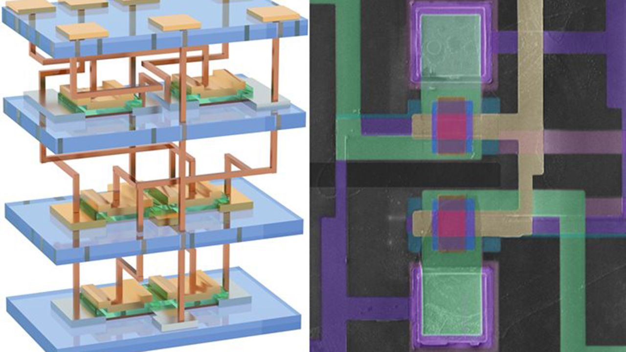
The massive hardware demands of artificial intelligence (AI) applications are stretching the physical and structural limitations of semiconductors. But researchers have engineered a three-dimensional silicon chip that they propose as the solution.

In a new study published May 27 in the journal Nature, scientists found a way to cram more computing power into a chip by stacking silicon circuits in multiple layers in a way that doesn't impact performance.

Stacking chips vertically, known as 3D integration, is more efficient than traditional 2D chips, where silicon circuits are spread across a single surface. This is because stacking shortens the distance that data has to travel and reduces the power required for data transmission.

The researchers' 3D chip uses ultrathin silicon membranes and low-temperature manufacturing techniques to overcome the challenges of current chip architectures.

"Our method is not only easier to implement with lower cost, but it has several advantages over previous approaches to stack silicon wafers," Qing Cao, first author of the study and a materials science and engineering professor at the University of Illinois Urbana-Champaign, said in a statement.

Extending Moore's law

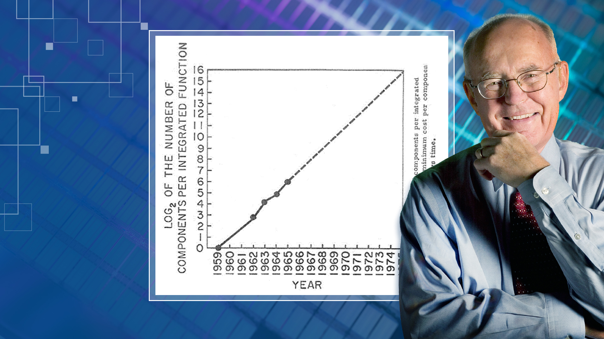
Since the 1960s, ensuring that electronics can handle more demanding applications has meant making transistors smaller so more can be packed onto a single chip. But, as Cao pointed out, doubling the number of transistors every couple of years β€” a principle known as Moore's law β€” is becoming less feasible.

"If you look at the actual size of transistors, they're not getting smaller, especially in terms of their contacted gate pitch," Cao said in the statement β€” defined as the combined width of one transistor gate and the space needed to separate it from the next.

"This is because we're becoming limited by the intrinsic material properties of silicon and the fundamental rules of quantum mechanics. If we're going to keep up the trend of increasing processing power of our microprocessors, we have to start thinking beyond just squeezing more devices on a single surface."

The researchers think vertical integration across multiple layers is the best way to guarantee that engineers can continue to adhere to Moore's law, because this approach creates room for more transistors on a chip.

"Today it takes six microelectronic devices called transistors on a single plane to store one bit of information," Cao explained, suggesting that just like in a densely populated city, the only way to solve overcrowding is to build upward. "You get the same functionality, but the spatial footprint is reduced while making communication between layers faster and more efficient."

Gordon Moore photographed beside a graph representing Moore's Law.

Scientist Gordon Moore seen with a graph representing Moore's Law. (Image credit: Intel)

Getting around the heat problem

Stacking is nothing new, of course, but vertical integration β€” building layers directly on top of one another β€” can create thermally dense packages. In the study, the researchers noted that the fabrication of high-quality silicon chips demands temperatures up to 1,832 degrees Fahrenheit (1,000 degrees Celsius).

However, once the first chip layer has been completed, the metal wiring introduced to connect further layers can be destroyed by such high temperatures. As a result, the "thermal budget" β€” the maximum amount of heat that can be endured before degradation starts to occur β€” for any additional layers is 752 F (400 C), said Cao. This can result in performance and reliability issues.

When creating 3D stacked silicon chips, manufacturers have sought to avoid this problem by using alternatives to single-crystalline silicon for the upper layers, according to the researchers. These materials include amorphous and nanocrystalline metal oxides, carbon nanotubes and polycrystalline silicon, but they can lead to performance and reliability issues, the scientists said in the study.

To overcome this challenge, Cao and his team adopted an approach called "monolithic integration" β€” a process in which all chip components are fabricated on a single piece of substrate, as opposed to making them separately and then bonding them together later.

To build each chip, the researchers created ultrathin silicon nanomembranes that they then transferred, using a roll laminator, onto a substrate containing the bottom layer.

The maximum temperature required to generate a strong bond using this method was just 392 F (200 C) β€” five times less than the heat normally required. The membranes they transferred were also just 10 nanometers thick or less β€” about the size of a protein β€” compared with the approximately 500-to-700-micrometer (500,000 to 700,000 nanometers) thickness of a typical wafer. Because they are thin, these membranes are mechanically flexible to conform to the underlying surface, Cao added.

The result of this process was a 3D chip with three layers, each containing 625 transistors. This pales in comparison to the billions of transistors that can be crammed onto chips already on the market, but the researchers believe their technology boasts power efficiency benefits. The electrical current that can flow through the chip has proved to be at least three to four times greater than that of monolithic chips made from alternative materials.

The big question is whether their 3D silicon chip can make the leap from the laboratory to commercial applications. While the research demonstrates the potential of a chip comprising three stacked layers, the scientists suggested that plenty more layers can be added in future iterations.

Can you match these ancient devices to their pictures? Find out with our computing quiz!

  •  

Scientists figured out how to shrink huge ultrafast lasers so they fit on a tiny chip β€ͺβ€ͺ—‬ the 'holy grail' of the field

A breakthrough in photonic chips could make large, costly, ultrafast lasers dramatically smaller, leading to portable and affordable imaging, diagnostic and information-processing devices, researchers say.

By using a decades-old overlooked laser architecture, scientists managed to fit an ultrafast laser onto a tiny photonic chip β€” a chip that uses light, rather than electricity, for computing operations.

In a new study published June 3 in the journal Nature, the team demonstrated that a tiny laser on the photonic chip could deliver 1.05 nanojoules of energy in 147-femtosecond (147 quadrillionths of a second) bursts β€” thereby competing with the output of laboratory-class ultrafast lasers.

Ultrafast lasers are used in a variety of applications, from precision manufacturing and eye surgery to biological imaging and atomic clocks, but the systems needed to power them tend to take up whole tabletops in labs or factories. Yet the powerful output of these laser pulses made them difficult to miniaturise onto photonic chips.

"For more than twenty years, a high-pulse-energy femtosecond laser on chip was widely regarded as a holy grail of integrated photonics," Tobias Kippenberg, a photonics professor at the Swiss Federal Institute of Technology(EPFL), said in a statement.

"Our result shows that it is not only possible, but that it can be achieved with a surprisingly elegant architecture that the integrated-photonics community had overlooked."

Forward-thinking breakthrough comes from looking back

Photonic chips manipulate light by using microscopic structures called waveguides β€” usually in the form of optical fibers or etched cavities β€” to carry information. They aren't particularly novel, and can be found in fiber-optic communications, medical sensors and lidar systems.

But photonic chips have previously struggled when handling high-powered, ultrafast lasers. That's because they need to contain light to extremely small waveguides, leading the light to interact strongly with itself and destabilizing the laser pulses.

To tackle this problem, the researchers looked at a laser architecture called the Mamyshev oscillator, created in 1998 by Pavel V. Mamyshev, a physicist and engineer at Bell Labs.

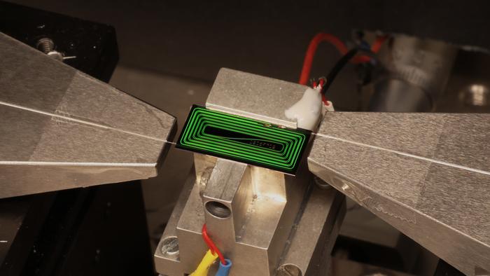
A close up of a chip on a metal platform.

EPFL's chip-based ultrafast laser operates in a testing set up. (Image credit: Zheru Qiu/EPFL)

This oscillator, which has received little attention in the world of photonic chips, works by placing a nonlinear waveguide between two optical filters. This causes a high-intensity laser pulse to expand into a broader range of colors that can then pass through both filters while weaker light, which can cause laser destabilization, is blocked out. This technique essentially means that a high-intensity laser pulse can be maintained.

Because the Mamyshev oscillator doesn't require extra components to manufacture on a chip, it presents an attractive design for use on photonic chips. And although the laser cavity needed to direct an ultrafast laser is 16.5 inches (42 centimeters) long, it can be folded to occupy around the same area as a match head. This can't be done with conventional fiber-optic-based lasers, often used in photonic chips.

That takes care of the size, but the cost of ultrafast laser systems is another challenge. But because photonic chips can be fabricated using silicon wafers in the same fashion as computer chips, more than 1,000 laser cavities could potentially be produced in a single batch, the researchers said. As such, photonic chips with ultrafast laser capabilities could be produced at scale, in turn reducing manufacturing costs and even expanding their use.

Photonic chips capable of handling ultrafast lasers could, in the future, lead to portable tools for tasks like detecting pollutants or performing advanced medical diagnostics in the field, the researchers noted in the study. The technology also opens the door to smaller atomic clocks that can benefit navigation and future communications.

  •  
❌