Researchers unlock high-res view of 2D materials by doing a microscopic twist
One of my favourite books about physics is The Second Kind of Impossible: the Extraordinary Quest for a New Form of Matter by Paul Steinhardt. It chronicles how the physicist and his colleagues established the extra-terrestrial provenance of a mysterious quasicrystal sample and then trekked to its likely place of origin in the Siberian wilderness.
That sample was first identified by the Italian geologist Luca Bindi, who features throughout the book and specializes in the discovery of new minerals. I was delighted to see that Bindi has a new paper out that identifies a hitherto unknown material. That excitement was tempered by the fact that the alloy was created by the catastrophic nuclear explosion over the Japanese city of Hiroshima.
On this day in 1945, an atomic bomb was detonated at 580 m over the city, creating a fireball where temperatures exceeded 7000 °C. As many as 140,000 people were killed by the bomb, which destroyed about 70% of the city’s buildings.
The fireball was a turbulent plasma of vapourized material from the city. This included building materials, metals, soil, water and, we mustn’t forget, some of the city’s residents. The plasma condensed rapidly creating glassy particles of micron–millimetre size that rained down on the Hiroshima area. These “hiroshimaite” particles mostly comprise of calcium, aluminium and silicon and can be found in the sandy beaches of Hiroshima Bay.
“The fireball left behind materials that never existed before,” says Bindi – who is based at the University of Florence. He adds that these hiroshimaites are helping scientists understand how matter behaves under extreme conditions – describing the fireball as a “giant accidental material-science laboratory”.
In this latest study, Bindi and colleagues in Italy, the US and Switzerland have identified a new metal alloy in a piece of hiroshimaite. The metallic grain is about one micron in size and is a homogenous mixture of six metals and silicon. X-ray diffraction shows that the alloy has an unusual crystal structure. This, along with the alloy’s high silicon content, make it a special material that has never been seen before.
According to Bindi, the alloy was formed by the condensation of a complex metallic vapour that was created by a range of materials that were caught up in the nuclear fireball. As the fireball cooled rapidy, a tiny droplet of metals and silicon condensed from the plasma. Then as the temperature dropped at an extraordinary rate, the droplet solidified and its metastable crystal structure was frozen in. This violent quenching prevented the alloy from evolving to a more common crystal structure.
This is not the first time that Bindi has found a new material in the debris of a nuclear explosion. A few years ago his was part of a team that discovered a quasicrystal in a piece of trinitite – glassy material that was created in July 1945 by the Trinity nuclear bomb test in New Mexico.
Bindi and colleagues report their results in Science Advances.
The post New material was created in Hiroshima nuclear explosion appeared first on Physics World.
The speed of laser light is due for a major upgrade after an international collaboration of scientists has developed a breakthrough nanomaterial. The new metasurface can steer and shape light beams at unprecedented speeds of just 74 quadrillionths of a second.
Scientists at UC Berkeley and Tel Aviv University revealed their new optical surface, developed in a Caltech lab, in a recent paper published in Nature Nanotechnology.
According to the team behind the breakthrough, their work will have ramifications for communications, sensing, imaging, and even quantum technologies, providing a new benchmark for “high-speed” light manipulation.
Since the fiber-optic advancements of the 1980s, lasers and light pulses have underpinned some of our most crucial cutting-edge technologies. Advanced computers, communications systems, sensors, and even the elusive quantum systems all rely on controlling light.
While the speed of light is so incredibly fast that physicists consider it a constraint on the maximum speed that matter can travel through the vacuum of space, the speed at which our technology reacts to it is far slower.
The scientists’ breakthrough metasurface contains silicon structures even smaller than the wavelength of light, resulting in an ultra-thin surface. Silicon’s optical properties change upon bombardment with laser pulses, a property that the team strongly enhanced with their nanostructure design. In their design, the properties of the material are modified via light pulses, which alter how the material influences a second beam of light impacting its surface. Notably, their metasurface allows for control of a beam of light without any moving parts, such as mirrors or lenses.
The team conducted laboratory tests in which they manipulated light beams by up to 13 degrees and reshaped them into different patterns.
“The key idea was to create a metasurface whose optical response is not fixed once it is fabricated,” said lead author Dr. Claudio Hail. “By changing the illumination pattern, we can reconfigure how the device steers and shapes light, and do so on an ultrafast timescale.”
“For me, the most exciting aspect is seeing an idea that had been with us for years become an experimental reality,” said co-author Dr. Lior Michaeli. “The ultrafast effect we wanted to use is naturally very weak. We had to design the metasurface so that it would amplify the effect enough not only to measure it, but to use it to steer and shape light.”
While the metasurface produced record-breaking speeds under laboratory observations, exactly how fast it can operate remains uncertain. The researchers note that the switching time and the duration of the laser pulse were extremely close, which indicates that quicker pulses could push the optical surface’s speed even higher.
One of the major potential advances that could come from this new metasurface includes systems that carry information primarily with light, end-to-end. Current communications systems use light to transmit messages, but those messages are converted into electrical signals for processing. By increasing the speed at which light can be manipulated, this would reduce the necessity to convert light signals into electrical ones, removing unnecessary actions in computing.
“This work points to a broader opportunity: using engineered structures to strengthen interactions between light and matter and turn them into tools for control, sensing, and information processing,” Dr. Michaeli said. “This is closely connected to research directions we are now pursuing at Tel Aviv University.”
Despite its promise, the work is still in the fundamental phase. Although not yet ready for practical use, the metasurface offers promise in future ultra-fast computing applications, where it may soon help to cut out the middleman of electronic conversion.
The paper, “Ultrafast, Reconfigurable All-Optical Beam Steering and Spatial Light Modulation,” appeared in Nature Nanotechnology on June 22, 2026.
Ryan Whalen covers science and technology for The Debrief. He holds an MA in History and a Master of Library and Information Science with a certificate in Data Science. He can be contacted at ryan@thedebrief.org.
One of the first schools to shut down after students were found making AI nudes of female classmates is now asking a court to toss a lawsuit filed by victims who claimed that the school stayed silent for months while the emboldened boys targeted many more girls.
In a motion to dismiss this week, Lancaster Country Day School (LCDS)—a private K-12 school in Pennsylvania with fewer than 600 students—argued that it was false to say the school never reported the harm to law enforcement. The tip that the school received came from the Pennsylvania Office of the Attorney General, which is itself a law enforcement agency, the filing said.
It’s also false to say the school knew that girls were being targeted, the school argued, because the tip did not mention any specific student victims.


© uniquepixel | iStock / Getty Images Plus
One of the most striking discoveries in condensed matter physics over the past few years is that simply rotating one atomically thin crystal on top of an identical layer can create entirely new electronic behavior. This idea became famous in 2018, when physicists found that graphene sheets stacked at a very particular “magic angle” could turn into a superconductor, even though a single sheet of graphene is not. That discovery launched an entire field, sometimes called twistronics, built around moiré patterns: the large-scale interference patterns that appear when two crystal lattices are laid on top of each other with a slight mismatch in angle or spacing. In many materials, these patterns reshape how electrons move, sometimes producing superconductivity or other exotic collective states.
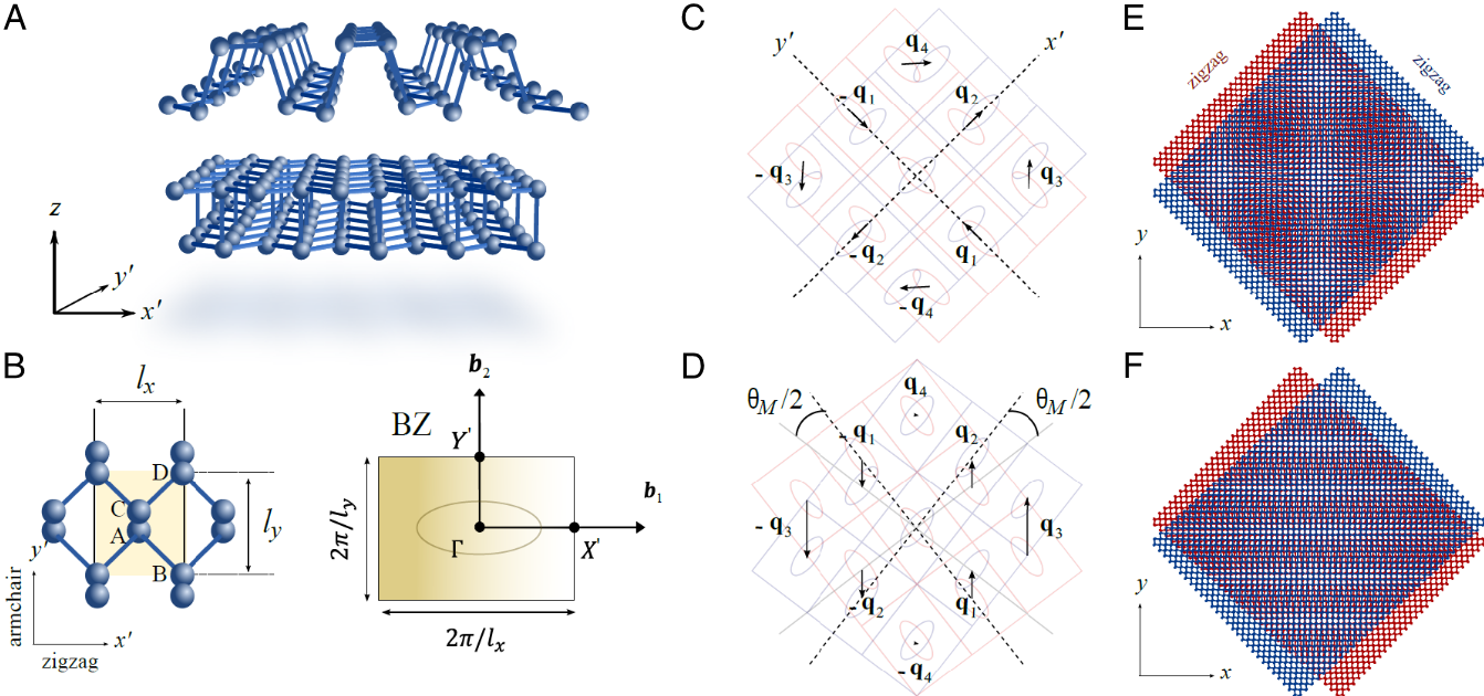
Most of this research has focused on materials whose crystal structure looks roughly the same in every direction, such as graphene, where the interesting physics shows up only at very small twist angles, close to perfect alignment. Now, a team of researchers instead looks at a strongly directional material: bilayer black phosphorus, whose atomic structure behaves very differently along two perpendicular directions in the plane, somewhat like a fabric that stretches easily one way but not the other. That built-in directionality turns out to change the whole logic of moiré physics, producing an effect the authors call moiré collapse. 1

In black phosphorus, the two layers start out rotated 90 degrees relative to each other. As that angle is dialed away from 90 degrees, the moiré pattern does something unusual. Rather than staying a two-dimensional pattern, like a slowly shifting checkerboard, it stretches more and more along one direction until, at a specific angle that depends only on the material’s own geometry, it effectively stops repeating in the other direction altogether. What remains behaves like a one-dimensional crystal, even though the material is still built from ordinary two-dimensional atomic sheets. For twisted bilayer black phosphorus, the calculations place this collapse at a twist of about 71.6 degrees, or equivalently about 18.4 degrees away from the initial 90-degree arrangement.
This transformation has nothing to do with how electrons repel or attract each other; it is pure geometry. The mathematical description of the moiré pattern, expressed in terms of the directions in which its periodicity repeats, is squeezed from two independent directions down to one. In ordinary space, this means the pattern keeps a well-defined repeat distance along one axis while stretching out indefinitely along the other, with no repeating pattern left in that direction at all.
Such a dramatic structural change reshapes the electrons riding on top of it. At the untwisted 90-degree configuration, the anisotropy of one layer happens to cancel out the anisotropy of the other, so electrons move about equally well in every in-plane direction. As the twist angle approaches the collapse point, that cancellation breaks down. The electron energy bands become sharply directional, and electrons increasingly travel along one preferred line rather than spreading across the plane. Their energy spectrum starts to show the telltale fingerprints of one-dimensional systems, including sharp spikes in the density of available electron states known as one-dimensional van Hove singularities.
One-dimensional conductors behave very differently from ordinary metals. In a three-dimensional metal, electrons can mostly be treated as independent particles that only weakly notice one another. Confine them to a single dimension, however, and that picture stops working: electrons cannot slip past each other, so they are forced to move collectively, in a coordinated wave-like fashion. The framework that describes this collective behavior, called Luttinger liquid theory, traces back to work by Sin-Itiro Tomonaga in 1950 and Joaquin Luttinger in 1963, and it has since been confirmed experimentally in systems such as carbon nanotubes. In a Luttinger liquid, the basic excitations are not single electrons at all, but collective ripples of charge and spin, and this leads to electrical transport properties that look qualitatively different from those of a normal metal.
The calculations in this study show that moiré collapse naturally sets up the conditions Luttinger liquid physics requires. As the collapse angle is approached, the one-dimensional electronic channels that form become progressively less coupled to their neighbors, making the correlated, wave-like behavior increasingly favorable. The analysis estimates a Luttinger parameter of about 0.3 for the collapsed black phosphorus system, a value indicating strong electron-electron interactions, and it predicts distinctive collective charge oscillations and unusual, non-metallic patterns in electrical conduction that could, in principle, be measured in the laboratory.
A notable feature of this mechanism is that the electron bands stay quite dispersive even at collapse, with electron speeds exceeding 100 kilometers per second. This sets it apart from most previously studied moiré systems, including twisted graphene, where strong correlations usually arise because the electronic bands become extremely flat and electrons effectively slow to a crawl. Here, the correlated behavior instead comes from the geometric collapse of the moiré lattice itself, with fast-moving electrons confined to one dimension rather than slow ones spread over two.
To test these ideas, the researchers combined simplified mathematical models with detailed first-principles calculations of the atomic and electronic structure. Beyond black phosphorus, they found the same collapse in twisted bilayer tin selenide, another layered material with strongly directional bonding. The details of the electronic structure differ somewhat because of the specific atomic orbitals involved, but the same geometric collapse into quasi-one-dimensional channels appears, suggesting the phenomenon is not a peculiarity of one material but a general consequence of twisting any sufficiently anisotropic crystal.
Taken together, the findings outline a different strategy for engineering exotic quantum matter. Instead of hunting for a special magic angle that flattens electronic bands, as in twisted graphene, this approach relies on a purely geometric collapse angle at which a two-dimensional moiré material naturally turns one-dimensional. If confirmed in experiments, it would offer a new and versatile platform for studying Luttinger liquids and other correlated electronic phases that only emerge when electrons are squeezed into moving along a single line.
Author: César Tomé López is a science writer and the editor of Mapping Ignorance
Disclaimer: Parts of this article may have been copied verbatim or almost verbatim from the referenced research paper/s.
The post Moiré collapse, when a twisted crystal becomes one-dimensional appeared first on Mapping Ignorance.

Many of today’s electronic devices — from the semiconductors in your cell phone to the photovoltaic cells in your solar panels — are built on thin-film substrates. The thin film is an electronically conductive material while the substrate is an inert material. Or is it?
Physicists and materials scientists have long assumed substrates do not react to electrical stimulus, but new research from the University of California San Diego Alex Frañó’s lab and a team of collaborators has shown that substrates are not inert after all. The discovery 1 has the potential to help engineers build the dense, three-dimensional, brain-inspired computer chips needed for more energy-efficient computing.

In a human brain, a vast network of neurons works across different regions, enabling every thought and action we take. Yet thoughts that are quick and simple for humans — recognizing faces, differentiating a cat from a dog or solving a captcha — can be devilishly hard and energy-intensive for computers. Quantum materials may provide a solution.
It was this quest to develop new materials that led Frañó’s lab to study vanadium dioxide thin-film devices. When a voltage is applied to the thin film, an electric filament forms — something similar happens when the Earth and atmosphere create a voltage strong enough to result in lightning. The filament in the thin film drives the device’s electrical spiking, much like the signals in our neurons.
This reaction has been studied countless times in labs around the world, but Frañó’s lab was implementing a new technique, developed by graduate student Elliot Kisiel, called dark-field X-ray microscopy. Kisiel, who spent most of his graduate studies at Argonne National Laboratory and is now a Mayer Postdoctoral Fellow there, developed the tool to combine the best of two worlds: electron microscopy and X-ray diffraction.
“Dark-field X-ray microscopy gives us the ability to look at an entire device in one image, which not only greatly improves how fast we can perform these measurements, but also allows us to study the areas surrounding the devices with high fidelity,” he stated.
Since the lenses for X-rays are often thick and, therefore, absorb most of the X-rays that pass through them, the team needed to look at something that provided more signal, which is why they decided to look at the substrate during some of their preliminary testing with this new technique.
What they saw was completely unexpected: not only was there a change in the thin film, but there was also a change in the substrate, showing for the first time that the two parts were sharing energy or “coupled.” This discovery went against everything scientists had assumed about substrates for decades.
Thin films are so called because they are vanishingly thin — around 100 nanometers — while the substrates they sit on can be 10,000 times thicker. Despite their lopsided sizes, in this experiment, the thin film was able to push and pull on the substrate. Frañó likened the discovery to a tree on a mountaintop being able to move the entire mountain. Furthermore, the substrate also acted on the thin film, each pushing and pulling on the other.
They spent the next four years making sure what they saw wasn’t a fluke. They not only reproduced the results doing the research exactly as they had done it the first time, but they also reproduced the results when they changed certain aspects of the sample, such as the thickness and material of the substrate. They also tested their results using different instrumentation. Much of that work was done at Argonne, which has a synchrotron facility that produces high brilliance X-rays, and at Brookhaven National Laboratory, home to the world’s only all-electric ultrafast electron microscope, which is able to capture exactly how a working device behaves under realistic operating conditions.
It wasn’t a fluke.
“The assumption that substrates are inert needs to be rethought,” Frañó stated. “Going forward, we have to assume that the substrate is undergoing changes when the film is. This is a transformational notion that counters decades of previous supposition.”
This paper is a companion to a paper that was published last year in ACS Nano 2. In that paper, they used dark-field X-ray microscopy to study the thin film, while this paper focuses on the substrate. Together they illustrate how one research result leads to the next research inquiry.
In Frañó’s case, the question he now asks himself is, “What can we do with this new substrate discovery? If a tree is moving the whole mountain, let’s find a way to capitalize on that.”
One idea is that the substrate can act as a medium that can couple materials on either end of the substrate. Currently, thin film devices are connected two-dimensionally, but if researchers could build on both sides of a substrate, it would allow for three-dimensionality, opening up the possibility of denser, more interconnected computer chips, and bringing us one step closer to the next generation of computing.
The post Substrate dynamics could power brain-inspired chips appeared first on Mapping Ignorance.

Breathing clean air depends on filters that do more than trap particles—they must hold them. In many conventional systems, captured dust can loosen under airflow and mechanical disturbances, which lowers filtration efficiency, shortens service life, and forces more frequent replacement. The bottleneck is not capture alone, but durable retention of what the filter catches.
A research team led by Professor Sanghyuk Wooh and Professor Chae Bin Kim has introduced a dynamic imine bond adhesive (DIBA) designed to keep airborne particles embedded. The concept is to marry solid-like stability with liquid-like adhesion, so the filter surface can “refresh” itself while working.
The coating is built by crosslinking polydimethylsiloxane (PDMS) via dynamic Schiff base chemistry. This chemistry enables bond exchange at the interface, allowing adhesive sites to reorganize over time rather than degrade into inert residue. The result is a coating that is both mechanically robust and chemically active.
When sprayed onto commercially available filter media, the DIBA layer behaves like an internal reservoir of stickiness. As particles are collected, they are drawn into the adhesive film rather than remaining only on the exterior fibers. Capillary-driven wetting then forms adhesive bridges around individual particulates, increasing the real contact area that governs holding strength.
Performance tests combined chemical, mechanical, and interfacial characterization—rheology, FTIR, atomic force microscopy, and microscopy—with filtration trials. The coating boosted particle adhesion dramatically, approaching a nearly seventy-fold improvement compared with typical behavior. Importantly, the adhesive renewal process helps counteract the gradual loss of attachment that plagues standard filters.
Filtration efficiency improved by roughly 10–30% across multiple commercial materials, without raising pressure drop. The upgrade is significant in practical terms: one reported shift is from MERV 6 toward MERV 11, indicating better capture at the same airflow penalty.
The coated filters also sustained operation under high-speed airflow (up to 20 m/s) and delayed pore clogging. By maintaining effective particulate capture for longer intervals, the DIBA approach extended filter lifespan by nearly a factor of two relative to conventional designs.
Because DIBA is applied through simple spray-coating, it is compatible with existing manufacturing and retrofit workflows. The researchers highlight applications ranging from HVAC and air purifiers to cleanrooms, industrial dust collectors, automotive cabin filters, and personal protective equipment.
More broadly, the work suggests a platform for next-generation filtration where energy use and replacement schedules improve simultaneously. The dynamic adhesive strategy could be adapted to other separations, including water purification and environmental remediation, wherever particles need to be captured and kept immobilized.
Subject of Research: Not applicable
Article Title: A Super-Adhesive Air Filter With Capillarity-Mediated Spontaneous Particle Absorption via Dynamic Bond Exchange
News Publication Date: 22-Apr-2026
Web References: https://doi.org/10.1002/adma.202600006
References: DOI: 10.1002/adma.202600006
Image Credits: Professor Sanghyuk Wooh from Chung-Ang University, Republic of Korea and Professor Chae Bin Kim from Pusan National University, Republic of Korea
Air filtration, dynamic adhesive chemistry, Schiff base, PDMS, particle retention, capillarity, MERV, particulate matter, surface engineering, polymers
Specially engineered materials known as metamaterials can boost heat transfer over nanoscale distances compared with conventional materials, thanks to the coupling of quasiparticles known as surface phonon polaritons. This new result, from researchers at Carnegie Mellon University, Stanford University and Purdue University, all in the US, could help improve technologies such as on-chip cooling and thermophotovoltaic systems.
The maximum radiative heat transfer between two macroscopic-sized objects at different temperatures can be estimated by assuming that the objects are “black bodies”. These are ideal entities that absorb all the radiation falling on them and emit thermal radiation according to Planck’s law. This approximation breaks down, however, when the objects are placed within a few hundred nanometres of each other. In this case, they begin to exchange heat much more strongly thanks to a phenomenon known as near-field enhancement, which can exceed the far-field black body limit by several orders of magnitude. This effect is already put to good use in technologies such as heat extraction and thermophotovoltaic systems.
Until now, near-field enhancement had only been observed and studied in naturally occurring materials, such as polar dielectrics, doped semiconductors and metals, explain the study leaders, mechanical engineer Sheng Shen at Carnegie Mellon and electrical engineer Shanhui Fan from Stanford. Although theoretical studies have predicted that metamaterials could surpass the performance limits of naturally occurring materials, there had not previously been any experimental demonstration of metamaterial-enhanced near-field radiative heat transfer. Identifying such metamaterials would be of great use as it would allow the effect to be exploited more widely.
Shen, Fan and colleagues observed enhanced near-field radiative heat transfer in a nanodevice platform comprising metamaterials based on arrays of gold split-ring resonators patterned on silicon nitride membranes. The researchers positioned the metamaterials so that they faced each other across a nanoscale gap, observing that heat transfer between them increased by as much as four times compared with similar setups using ordinary materials.
As well as confirming that radiative heat transfer is enhanced over short distances for these metamaterials, the results suggest that the interaction between metamaterials and surface phonon polaritons is responsible for the increase. These quasiparticles are produced by phonons, which are vibrations of the crystalline lattice, as they interact with oscillating electromagnetic fields at the material surface – in this case, those at the surface of the gold metamaterial structures. This coupling allows heat to tunnel across the gap between them and the silicon nitride membranes more efficiently – something that increases the energy flow between the two, explains Shen.
According to the researchers, the effect could help enhance and manipulate heat exchange at the nanoscale and could find applications in next-generation cooling for high-performance microelectronics, thermophotovoltaic systems for waste-heat harvesting and high-sensitivity infrared detection.
There are still a number of challenges to overcome before such applications see the light of day, however. On the theoretical side, notes Fan, the complex interactions between the metamaterial units and their supporting substrate make numerical calculations and analyses exceptionally difficult. “To address this difficulty, we have developed a numerical tool based on fluctuational electrodynamics to design the structures, alongside a coupled-mode theory model to fully elucidate the underlying physics,” he says.
Experimentally, measuring nanowatt-level radiative heat exchange across a sub-micron gap also demands extreme precision. The researchers tackled this challenge by designing an on-chip device using a “suspended thermal bridge” method that transforms the minute heat exchange into a measurable temperature rise. Indeed, they succeeded in detecting heat flow of less than 1 nW in these nanodevices.
They report their work in Nature.
The post Metamaterial boosts heat transfer on the nanoscale appeared first on Physics World.
Frost can spread not only along surfaces but also via suspended “ice bridges” that form above them. The discovery of this previously unknown frost-propagation pathway could lead to new ways of making surfaces that resist frost growth, thereby improving the performance of devices that operate in cold, humid environments.
Frost accumulation is a major problem in refrigerators, aeroplanes and heat pumps, to name just a few. On the microscale, it primarily spreads from one individual freezing water droplet to the next via two-dimensional bridges, or causeways, that temporarily form on the surface of an object. Although the wettability of the surface is known to affect the spreading process, the mechanism behind this effect was poorly understood.
To learn more, a team led by physicist Nenad Miljkovic at the University of Illinois Urbana-Champaign, US imaged the channel-forming process using high-speed high-resolution optical microscopy combined with a profilometry technique called focal plane shift imaging (FPSI). They found that frost can spread in two distinct ways. On hydrophilic surfaces, causeways form along the substrate, in line with current theoretical models. On superhydrophobic surfaces, however, the situation is quite different. Here, frost spreads via ice bridges that are suspended above the surface in three-dimensional space.
This suspended or “out-of-plane” growth mode represents a fundamentally different pathway for frost propagation, says team member Siyan Yang, the first author of a Nature Physics paper about the work. Previous studies likely overlooked this mechanism, Yang adds, because of limitations in experimental observations.
The researchers also studied the growth rate of the different bridge types. They found that suspended bridges grew slower than bridges on the surface due to the reduced thermal coupling between the bridges and the cold substrate. This reduced coupling correspondingly reduces the vapour pressure difference between ice and water droplets (which depends on surface droplet geometry, itself controlled by wettability) and drives down ice growth. Indeed, the team found that the speed at which frost spreads fell more than 80% in this mode.
To test the practical relevance of their findings, the researchers applied superhydrophobic coatings to metre-sized structures such as the finned-tube aluminium heat exchangers commonly found in air conditioners, refrigerators and automotive systems. Condensation frosting on such systems poses a major efficiency challenge because frost has an inherently low thermal conductivity. When it accumulates on heat exchangers, it therefore severely impedes heat being exchanged with the surrounding air.
On uncoated commercial heat exchangers that are inherently hydrophilic, the team found that frost rapidly forms and spreads across the fins. “In the superhydrophobic counterparts, however, the onset of frost formation is delayed, and it propagates much more slowly,” Yang says. In the two kinds of commercial systems they tested, she adds, applying superhydrophobic coatings nearly doubled the frost propagation time.
The results suggest that designers of anti-frost surfaces could benefit from trying this new strategy, Yang says. “Rather than focusing solely on delaying initial ice nucleation, surfaces could be engineered to control the geometry of ice-bridge growth and interrupt frost spreading, thereby improving the performance and energy efficiency of a host of equipment operating in cold and humid environments,” she tells Physics World.
The team is now investigating how surface chemistry and surface structures influence suspended ice-bridge formation and frost propagation. “We are also exploring ways to translate the fundamental mechanism into scalable anti-frost coatings and heat-exchanger technologies,” Yang reveals. “Ultimately, our goal is to establish predictive design rules that connect microscale ice-bridge dynamics with real-world frost management performance.”
The post Frost spreads across surfaces via suspended ‘ice bridges’ appeared first on Physics World.
A new glass screen containing nanoclusters of copper iodide could create higher-resolution X-ray images using a much lower dose of radiation. The scintillating screen, which also works underwater, can be moulded into curved shapes, overcoming key limitations of the conventional rigid, flat-panel detectors used for many medical imaging applications. These include mammography, say the researchers at King Abdullah University of Science and Technology (KAUST), Saudi Arabia, and the University of Hamburg, Germany, who developed it.
X-ray scintillators capture X-rays passing through an object and convert them into flashes of visible light to form a digital image, explains physicist Mehmet Bayindir of KAUST and the University of Hamburg. The more efficient the scintillator is at this conversion, the clearer the final image and the lower dose of radiation required to generate it.
He and his colleagues’ detailed analyses of a scintillator containing nanoclusters of copper, iodine and an organic ligand revealed a fascinating phenomenon: its photoluminescence and radioluminescence pathways appear to have distinct physical origins. This implies that the scintillating light yield – that is, how much visible light a material emits when struck by high-energy X-rays – can be separated from its standard photoluminescence quantum yield (how efficiently the material converts absorbed ultraviolet or visible light into a different wavelength of light).
Until now, Bayindir explains, it was assumed that a material must have high photoluminescence efficiency to perform well when excited by X-rays. “Breaking this assumption directly challenges conventional wisdom and opens up a promising new design space for making high-performance scintillators – provided that materials highly responsive to radiation can be engineered of course.”
In recent years, researchers have been looking into cubane-type [Cu4I4L4, L: organic ligand] nanocluster glasses (NCGs) for use in this context. These belong to a family of hybrid transparent luminescent amorphous materials that show much promise for X-ray scintillation applications.
In their latest work, detailed in ACS Energy Letters, Bayindir and colleagues studied several stable alkyl-phosphine ligand-based NCGs. In these amorphous zero-dimensional quantum systems, ionizing radiation is mostly absorbed by the heavy iodine and copper elements at the cluster cores. The researchers used these NCGs to make large-area, free-standing scintillating screens – both planar and conformal – with ultrasmooth surfaces, using a fabrication methodology that they developed in their lab.
The screens are robust and can image samples – both electronic and biological – with sub-3 µm spatial resolution. They also work underwater, something that is difficult for conventional screens. The researchers demonstrated this by capturing a very clear scan of a fish’s tail in water that was indistinguishable from an image taken in air.
Such a glass scintillator represents a significant milestone, says team leader Osman Bakr. “Indeed, the level of precision we obtained allows us to capture highly detailed, high-contrast X-ray images of complex internal microstructures, such as the delicate anatomy of a microscopic insect and an electronic memory card, to cite but two examples,” he says.
“Combined with the fact that this new nanocluster glass becomes almost rubbery when heated to 42 °C, we can mould it into any three-dimensional shape at low temperatures,” study lead author Bashir Hasanov adds. “This could allow for X-ray imaging systems that curve to fit a person’s body and overcomes the limitations of conventional rigid, flat-panel detectors.”
One possible application is in mammography, he notes. Today, a major drawback of current mammography machines is that breast tissue must be firmly compressed between flat panels so that it can be imaged. This is very uncomfortable – and even painful – and deters many women from going for a scan.
“One in 20 women around the world will be diagnosed with breast cancer in their lifetime, with annual cases projected to reach 3.2 million and related deaths climbing to 1.1 million by 2050,” says Bayindir. “Many of these fatalities stem from late-stage diagnosis.
Nearly one-third of women miss their initial mammogram appointments, something that significantly increases their risk of succumbing to the disease. “While the reasons for this vary, the medical literature frequently cites the physical discomfort of tissue compression,” says Bakr. “What is more, because current guidelines recommend starting routine mammography screenings at age 40, cumulative lifetime exposure to X-ray radiation remains a clinical concern for many. Our long-term objective is to completely redefine this clinical experience.”
Indeed, the researchers say they would now like to bring this quantum glass out of the lab and into real-world applications. Bakr tells Physics World that his team’s immediate next step is to scale up the geometric dimensions of its mouldable screens while maintaining perfect thickness and clarity. “This would move us closer to full-scale clinical prototyping for 3D conformal medical imaging.”
“We are also designing a novel detector architecture capable of high-resolution imaging on curved surfaces using an array of specialized optical sensors,” he reveals.
The post Mouldable glass screen could make mammograms clearer and much more comfortable appeared first on Physics World.

Thanks to a novel encapsulation technique, researchers at Fudan University in Shanghai, China, have succeeded in imaging the surface structure of the atomically thin topological quantum material MnBi2Te4 (MBT) for the first time. The work could help advance our understanding of the intrinsic properties of this technologically important class of materials and enable their use in novel devices.
The electronic, magnetic and topological properties of materials thinned down to atomic-scale thicknesses are very different to those of their bulk counterparts. They can, for example, be employed to study exotic quantum states that could prove useful for a host of advanced applications, such as next-generation spintronics and dissipationless electronics.
Before such devices see the light of day, however, we need to understand these emergent properties, which means accurately determining the surface atomic structure of these materials. This is no easy task because these surface structures are extremely sensitive to their environment. What is more, the most common technique used to study them, transmission electron microscopy (TEM), requires samples to be prepared as lamellae, which degrades them, changing their structure. The high-energy electron irradiation beam in the microscope does them no good either.
In the new work, a team led by Yuanbo Zhang of the State Key Laboratory of Surface Physics and department of physics at Fudan University, studied the topological quantum material MBT. This is the only intrinsic magnetic topological insulator made in the laboratory so far and can be used to study novel topological states – such as the quantum anomalous Hall effect and axion-insulator physics – many of which are fundamentally governed by surface states.
Like other sensitive 2D materials, explains study co-author Jingjing Gao, MBT’s surface is exceptionally vulnerable to external perturbations, such as ambient air exposure, heat or standard electron microscopy preparation. These degrade the surface layer and irreversibly alter its structure. Indeed, a previous TEM study also revealed that the septuple-layer structure of an MBT flake transforms into a Bi2Te3-like quintuple layer configuration under ambient conditions.
To overcome this problem, Gao and colleagues developed a protective encapsulation technique that successfully shields the delicate surface structure of MBT from its environment and protects it during TEM sample preparation.
The researchers examined two types of encapsulating materials. The first was hexagonal boron nitride (hBN), which is chemically inert and already routinely employed to protect 2D materials. The second was a thin flake of MBT itself, which provides a “homomaterial” capping layer. They encapsulated the MBT in one of these two materials immediately after they had exfoliated (or shaved off) flakes of MBT from a bulk sample. They did this inside an inert argon-filled glovebox.
The protective layer acts like an atomic-scale barrier that isolates the MBT surface from oxygen, moisture, ion-beam damage and other environmental disturbances produced during the focused-ion beam processing used to prepare the samples for TEM. It also protects the MBT from the high-energy electron irradiation in the imaging microscope.
The researchers found that the homomaterial encapsulation is especially protective because the atomically similar layers can intimately contact with a minimal interfacial gap.
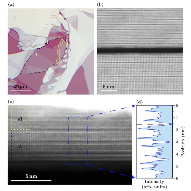
The technique strongly reduces defect formation, so the original lattice structure remains stable throughout the entire TEM workflow, explains Gao. “We therefore succeeded in safeguarding the ‘true’ surface throughout, allowing us to visualize the intrinsic septuple-layer structure at atomic resolution for the first time.”
The work will be important for both understanding intrinsic magnetic topological insulators and for developing quantum devices from these materials in the future, she tells Physics World. “Making such devices will demand exceptionally stringent requirements for sample surface and interface quality. This is because the MBT’s unique topological and magnetic properties are hosted by its surface states and even minor atomic reconstruction can distort its intrinsic quantum behaviour.”
Looking ahead, the researchers, who detail their work in Chinese Physics Letters, say they will now be looking to construct heterostructure devices with high-quality intrinsic surfaces and interfaces based on MBT. They will also make use of their encapsulation strategy to fabricate and study magnetic topological heterostructures.
“We will also explore topological superconductivity by interfacing MBT with superconductors, thereby advancing the development of topological quantum computing platforms,” reveals Gao.
The post Encapsulation enhances surface structure imaging of 2D quantum material appeared first on Physics World.
Altermagnets can transfer their unusual magnetic properties to nonmagnetic materials placed next to them, say theorists in China and the US. This so-called “proximity effect” had already been observed in ferromagnets and superconductors, but it is new for altermagnets, which were only recognized as a distinct class of magnetic materials in 2024. If confirmed experimentally, the team says the effect could aid the development of advanced quantum materials with applications in fields such as spintronics, valleytronics and fault-tolerant quantum computing.
In ferromagnets, proximity effects make it possible to tune properties such as magnetic anisotropy, coercivity and exchange bias in nonmagnetic materials that have acquired magnetic polarization from a neighbouring ferromagnet. Similarly, ordinary materials that have picked up superconducting correlations from a nearby superconductor are a mainstay of experiments on topological superconductivity and topological quantum computing.
In the latest research, physicists led by Tong Zhou of the Eastern Institute of Technology in Ningbo sought to understand whether altermagnets could likewise transfer their behaviour to a neighbouring material. To do this, they created a model of a van der Waals bilayer heterostructure in which the bottom layer is a two-dimensional (2D) altermagnet, V2Se2O, while the top layer is a non-magnetic semiconductor, PbO.
Zhou explains that the vanadium atoms in V2Se2O form two opposite-spin sublattices that are connected by rotational symmetry rather than by simple translation or inversion. This complex structure is what gives V2Se2O its characteristic altermagnetic spin splitting, with a band structure in which spin-up and spin-down electrons have different energies that vary in periodic patterns. V2Se2O also has a so-called spin texture, which is a pattern of spin polarization that produces a net zero magnetization in the material.
Using first-principles calculations, the researchers found that the distinctive symmetry-patterned magnetism of V₂Se₂O can indeed transfer into the PbO layer across the interface between them. As a result, Zhou says the originally spin-degenerate bands of PbO develop a clear momentum-dependent spin splitting.
Importantly, this pattern is not arbitrary. Instead, it follows the symmetry expected from the altermagnetic order of V2Se2O. What is more, the real-space spin density of the PbO mirrors the symmetry of the V2Se2O, showing that it has inherited altermagnetism rather than simply becoming generically spin polarized.
When the researchers rearranged the V2Se2O into a conventional antiferromagnetic configuration with no alternating spin splitting, they found that the induced splitting in PbO disappeared. They also observed that the degree of induced splitting decreases when the PbO is placed further away from the V2Se2O, confirming the proximity effect.
As a final piece of evidence, the researchers searched for similar proximity effects in other altermagnetic systems, ranging from insulators to metals and covering material platforms with 3D architectures as well as 2D ones. “Even graphene, one of the most common 2D materials, can acquire altermagnetic characteristics when interfaced with CrSb, which is an experimentally well-established altermagnet,” Zhou notes.
One of the work’s main implications is that altermagnets could be used to generate spin patterns in many otherwise non-magnetic materials, Zhou tells Physics World. “This means that instead of searching only for intrinsic altermagnets, we can now design ‘proximitized’ altermagnetic systems by combining an altermagnet with a semiconductor, metal or superconductor,” he says.
In semiconductors, Zhou notes, the altermagnetic proximity effect can induce controllable spin and valley splitting, which are promising for spintronics and valleytronics devices, respectively. In superconductors, meanwhile, the effect can generate momentum-dependent spin splitting without the need to apply an external magnetic field or introduce net magnetization – something that Zhou says offers a new route toward topological superconductivity and the Majorana modes that could revolutionize fault-tolerant quantum computing. “More generally, this effect provides a versatile platform for designing field-free spin devices, topological quantum devices and multifunctional van der Waals heterostructures,” he says.
Looking ahead, Zhou and colleagues say they would now like to observe the altermagnetic proximity effect in heterostructures fabricated in the laboratory. They also want to find out how to control the strength of the effect – for example, by changing interlayer spacing, stacking, strain, gating and possibly even layer twisting.
“More fundamentally, an important question is how fast and how reversibly altermagnetic order, and therefore the altermagnetic proximity effect, can be reconfigured dynamically,” Zhou says. “That would be especially interesting for controlling spin-dependent transport and topological phases in real time.”
The research is described in Physical Review Letters.
The post Altermagnets can turn neighbouring materials altermagnetic, too appeared first on Physics World.
Confine a liquid to a region a millimetre or less in size, and you’re in the weird world of “microfluidics” – where surface tension and capillary action dominate in ways we easily overlook from our macro-scale vantage point. Despite being a term that was coined only in 1992, the underlying phenomena have been with us for millennia, as Albert Folch argues in How the World Flows: Microfluidics From Raindrops to COVID Tests.
Folch, who is a professor of bioengineering at the University of Washington in the US, has spent his career developing microfluidic devices that exploit the peculiar properties of flows at this scale. In this book, he now steps back to admire the full scope and impact of microfluidics, revelling in droplets that form rainbows, deliver inhalable asthma medications, make up salad dressings and cosmetics, and print scaffolds of living tissue to aid patients’ healing.
I particularly enjoyed Folch’s ode to the Olmec – Indigenous people who lived in Central America from about 1200 BCE to 400 BCE. They would harvest latex from Panama rubber trees by tapping the bark and collecting the liquid drop by drop before the day’s heat caused the latex to coagulate and seal the cut. The Olmec even had their own version of vulcanization – the process that makes rubber elastic – using the juice of morning glory vines to process the sap into bouncy elastic balls, stretchy bands, shoe soles and raingear.
The Olmec spread their knowledge to neighbours as well. In fact, the name “Olmec” comes from the Aztec language and literally means “the rubber people”. Like the maple sugar industry – which gets its own historical treatment from Folch – the Olmec latex harvest relied on a tree’s vascular system, made up of narrow 25 µm capillaries that carry liquids like water, sap, resin and latex to nourish and defend the tree. Although the Olmec civilization eventually declined, their technology and ingenuity lived on, impacting the entire world.
Folch walks readers not just through the physics and biology of these systems – capillary rise, photosynthesis, transpiration – but through their human impact, too. He includes wonders, such as natural rubber powering a Victorian-era craze that brought us tyres, inflatable boats, children’s dummies (pacifiers) and other objects. Folch also covers darker stuff, such as the British businessman Henry Wickham (1846–1928) who smuggled thousands of rubber tree seeds out of the Brazilian Amazon to establish plantations in Africa and Asia, where he could exploit cheaper labourers.
Another chapter begins in the mountains near Granada, Spain, where villagers are rebuilding acequias – open-air waterways originally built by the Moors in medieval times. For nearly 1000 years, acequias turned the arid slopes into terraced fruit gardens by diverting snowmelt toward agriculture and recharging the groundwater. Water seeps downward through the acequia’s dirt bottom, protecting it from evaporating in the hot Sun and feeding aquifers.
As Folch notes, aquifers contain nearly 30% of Earth’s freshwater – far more than is found in rivers and lakes, which make up less than 1% of the total. But in the US alone, industrial agriculture has been draining aquifers at rates as high as 60 cm per year, far exceeding the slow percolation of rainfall into these underground reservoirs.
In fact, aquifers take hundreds or thousands of years to recharge, which, Folch notes, means a depleted aquifer effectively ceases to exist for those of us living now. Without acequias and other dedicated efforts to replenish aquifer levels through microfluidic flow, today’s corn fields will soon turn to dust.
How the World Flows charts the history of other unexpectedly microfluidic technologies too. Candles, for example, carry their fuel to the flame by capillary action along the wick. Then there’s paper, which soaks up ink through capillary action. Among more recent microfluidic inventions, Folch offers special laurels to the ballpoint pen, of which BIC alone has sold over 100 billion units since 1950.
Folch also takes care to introduce readers to many microfluidic medical devices, which might not be as widespread as ballpoint pens, but are perhaps more important. They range from dialysis machines that clean blood for failing kidneys, to COVID tests and continuous glucose monitors that let diabetics manage their blood glucose levels – a microfluidic technology that’s critical in my own home.
Folch describes the microfluidic devices that enable the Human Genome Project, as well as prototype instruments that could one day catch cancer cells through a simple blood screening. He also covers devices that could pick the perfect personalized drug cocktail for treating a patient’s tumour by studying their biopsied cells.
The most stunning microfluidic device Folch describes may be us
But the most stunning microfluidic device Folch describes may be us. As he argues, we ourselves are microfluidic. From our lungs to our cardiovascular system, from our lymphatic system to our sweat glands, our bodies rely on flow through tiny vessels.
Our bodies make up for diffusion’s slow pace by operating in parallel. Like the many co-operating central-processing units in a supercomputer, our bodies absorb oxygen through 500 million micro-sized alveoli in our lungs. We hear through ears equipped by microfluidics to act as both microphones and accelerometers. Our kidneys clean some 200 litres of blood a day – sending two litres of urine to our bladders as they do – through massively parallelized filtration.
Throughout How the World Flows, Folch’s enthusiasm for his subject shines. His approach is that of a storyteller, rather than a scientist, and the book is all the better for it. Whether readers are microfluidics experts or not, they will walk away with new stories to tell. (Don’t skip the footnotes…)
Although Folch’s stories are wide-ranging and entertaining, he stumbles at times with the overarching narrative. Some transitions are rough, and it’s not always clear why he’s chosen to order the stories in the way they’re presented. Nevertheless, his book is a fun and highly readable introduction to microfluidics that’s sure to entertain lay readers and excite a new generation of microfluidic engineers.
The post The wonderful world of microfluidics appeared first on Physics World.

Photonic glasses containing gold-cored, silica-shelled nanoparticles can produce high-purity colours across the visible spectrum. Crucially, the colours are independent of viewing angle. Developed by researchers in Korea, their design avoids the short-wavelength scattering that has prevented the attainment of a true red – and blurred other colours – in previous photonic glasses.
Synthetic materials are usually coloured using pigments, such as those found in dyes or paints. A pigment has a chemical composition that causes it to reflect light at certain wavelengths and absorb light at other wavelengths. Nature, however, makes widespread use of structural colour, whereby the physical structure of a material dictates which wavelengths are reflected and which are absorbed. A familiar example is iridescence, which is responsible for rainbow-like colours on some plants and animals.
Creating colour using structure rather than chemistry has several advantages. One is that there are no chemical chromophores to be bleached by sunlight, so the colour tends to be more durable. Another benefit is that there is no dye to leach if the material comes into contact with water or another solvent.
While structural colour can be created using traditional photonic crystals, these can be tricky to produce controllably. Moreover, a surface that relies on interference effects is inevitably iridescent – which means that its colour changes with the viewing angle.
One solution is colloidal photonic glasses, which are not physically textured but have particles such as silica or polymers dispersed throughout them with short-range order. These can be produced simply by solution processing, and their colour does not vary with viewing angle. The principal problem with these glasses is the attainment of colour purity – especially in the red. The challenge is that the glasses scatter light more effectively at shorter (bluer) wavelengths owing to Rayleigh scattering. This effect makes the sky appear blue and adds unwanted blue light to structural colour.
In the new work, nanophotonics expert Seungwoo Lee of Korea University in Seoul and colleagues synthesized 230 nm core–shell nanoparticles in which silica surrounds a 20 nm gold cluster. This has a plasmonic resonance that absorbs shorter wavelengths. The researchers then dispersed the nanoparticles in ethoxylated trimethylolpropane triacrylate. This is a photocurable resin that has a very similar refractive index as the nanoparticles. The resin was applied to surfaces by painting or solution deposition and then cured under ultraviolet light.
The resulting photonic glass scatters red light randomly, while absorbing shorter wavelengths. Lee stresses that this is different from a traditional paint. “The reflected colour is determined by particle size, spacing, refractive-index contrast, and the degree of structural order, rather than by a molecular chromophore alone,” he says. When the researchers reduced the size of the nanoparticle shells, first to 180 nm and then to 160 nm, they found that they packed more closely together, producing first green and then deep blue colours.
The explanation for the blue scattering is more subtle than for the red: “The gold core is not needed to ‘make’ blue in the same way that a blue dye would,” explains Lee. “However, the gold core can still improve perceived colour purity by reducing broadband diffuse scattering and nonresonant background light.” explains Lee “Without this suppression, silica-only photonic glasses tend to look milky or whitish because many wavelengths are scattered together.”
The researchers are now exploring several possible extensions of their research. They believe that the work could provide easily applied coatings that are durable as the light scattering comes from within the material structure rather from than a surface pigment.
They also believe it could have anti-counterfeiting properties: “In a normal ink or paint, its colour mainly originates from chemical pigments or dyes,” says Lee; “Our material produces a nanoscale structural signature: a specific reflectance spectrum, bandwidth, angular response, and microstructural arrangement determined by the particle diameter, core–shell geometry, refractive-index matching, volume fraction, and assembly pathway. This gives several possible authentication handles.”
Lee believes that it should be possible to reduce the cost of the material using a metal that is cheaper than gold. However, the precious metal is only 0.022% of the film by weight, so the technology may already be economically viable.
The film is described in Proceedings of the National Academy of Sciences.
“I think it’s really neat,” says materials scientist Aaswath Raman of the University of California, Los Angeles. “The concept of structural colour has been around for a really long time but to me it’s, like, the last steps before we see it out it the real world.”
He says the largest problems he foresees are the simple economics of competing with industrially-optimized paint industry – even if the technology is, in principle, superior. Nevertheless, he says, “of the technologies we see in research this is likely quite a good candidate for commercialization”. The next step, he says, is to actually find a “first use” application – he suspects the aerospace industry, which values ultralight, durable coatings, could be a candidate.
The post Photonic glasses deliver angle-independent structural colour, including reds appeared first on Physics World.
In today’s technologies, mechanical mechanisms generally provide the brawn while electronics supplies the brains. This is partly because it is challenging to write information into mechanical memories without resetting each bit individually. However, that could change as researchers led by Pedro Reis at École Polytechnique Fédérale de Lausanne in Switzerland and Martin van Hecke at AMOLF in the Netherlands have now found a practical means of writing mechanical bits. Their technique, which they describe in Science Advances, uses structures that resemble children’s slap bracelets placed on a rotating turntable. While they acknowledge it is unlikely to replace electronic memories, they argue that it could have specialist applications and might produce insights that translate into electronic innovations.
“The framework we propose could be very useful, for example, in the domain of physical intelligence, where you provide hardware with capabilities that don’t require essentially a brain or an electronic control system to do individual tasks,” Reis says.
Reis and van Hecke’s interest in mechanical memory stems from their research on metamaterials, which are materials that are defined not just by their composition, but also by the structures within them. Mechanical systems offer a tangible means of getting to grips with the complex behaviour of these metamaterials. “Often, all sorts of things that we do rely on nonlinear responses,” van Hecke notes, adding that such responses are much easier to study in mechanical systems than in optical devices.
A metamaterial made up of an array of switchable mechanical elements could function as a form of mechanical memory. However, to be practical, it needs to be possible to flip the states of individual mechanical bits using global controls, as opposed to addressing them individually. Otherwise, writing data will be very fiddly.
A solution emerged from Reis’ interest in rotating platforms, which he describes as “a very versatile way of loading mechanical systems”. While the pair had been friends for more than two decades, they had been working independently until, during a visit, the penny dropped and they realized that placing the metamaterial array on a rotating platform could provide the control they needed.
Because the angular velocity of the platform sends its momentum outwards, each mechanical object experiences a force in the radial direction, known as the centrifugal force. If this angular velocity is not constant, the object will experience an additional force in the orthogonal azimuthal direction, known as the Euler force. “So you have a complex force and bi-directional field that is highly tuneable,” says Reis. “And this tuneability is what we realized is very powerful.”
To construct their array, the researchers used clamped beams with two stable mechanical states – a little like a slap bracelet can be coiled up or flat, except these beams could either curve to the right or to the left. To individually address different beams, they ensured that each beam was unique in its width, the angle it was clamped at, and so on, all of which affect how much force is needed for a beam to ping into the opposite state. By tuning the parameters of each clamped beam and the angular acceleration of the rotating platform, they could engineer the applied force to switch (or not switch) specific beams, thereby writing data into the array purely by rotating the platform.
Doing this accurately requires a level of precision in acceleration control that surpasses what standard lab motors can achieve. However, the researchers say they were able to team up with a local company that had designed high-spec rotating platforms for its high throughput silicon chip production process. By programming platforms with five tailored clamped beams and the right rotation functions, they showed they could write the letters of the alphabet in ASCII script.
“This is a significant advance because it points toward future smart devices and robots that can be reprogrammed remotely without complex wiring or electronics, using only carefully designed motion‑based signals driven by a sole dynamic driving strategy,” explains Damiano Pasini of McGill University, Canada, who studies systems for mechanical computing but was not involved with this work directly.
Reis says he is excited about the scalability of the approach and its potential in high throughput experiments. Meanwhile, van Hecke is looking into how the idea might transfer to other systems, such as applying engineered force functions to crumpling sheets of complex glasses. “It just opens up possibilities for both studies, really fundamental studies of complex systems, but also real applications where you use this dynamic idea,” he tells Physics World.
The post Physicists create mechanical memory device from slap-bracelet-like structures appeared first on Physics World.
Quantum materials could transform technologies ranging from powerful computers and highly secure communications to advanced energy systems, but one major obstacle has long stood in the way. Most quantum materials reveal their unusual properties only when chilled to temperatures near absolute zero. At room temperature, continual atomic vibrations caused by heat can overpower the fragile [...]