❌

Reading view

Quantum Photons Survive a 24-Kilometer Journey Through Chicago’s Busy Internet

Data Security Quantum Internet InformationResearchers achieved the first real-world demonstration of quantum entanglement over a busy telecommunications fiber network. A single photon carrying quantum information had to travel more than 24 kilometers through an optical fiber already crowded with powerful internet signals. Despite the noise, it reached downtown Chicago still entangled with its partner at Northwestern University’s Evanston campus. [...]
  •  

The Bayeux Tapestry: how optical techniques have let this artwork come home

The Bayeux Tapestry
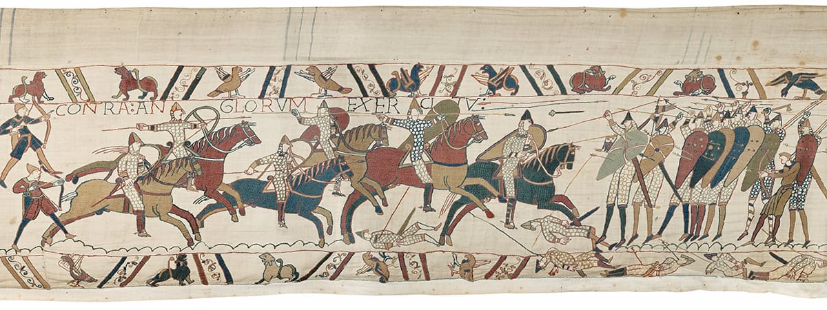
History in the making The Bayeux Tapestry is on display at the British Museum in London until July 2027 but you can view it for free online thanks to advanced optical imaging techniques. (Courtesy: © La Fabrique de patrimoines en Normandie, Antoine Cazin)

A few years ago, I was lucky enough to see the Bayeux Tapestry – the famous embroidered cloth depicting the Norman invasion of England in 1066. More than 900 years old, this historic piece of art is only 50 cm wide but more than 68 m long. It’s also extremely fragile, which why I was astonished when I heard that the Bayeux Tapestry was going to leave its home in Normandy and be transported across the English Channel to the UK.

The loan of the artwork, which was agreed between former British prime minister Keir Starmer and French president Emmanuel Macron last year, has now taken place. The tapestry arrived under police escort on 10 July and will be on display at the British Museum in London from September 2026 until July 2027. It is the first time the tapestry has been back in England, the country where this linen cloth was originally made.

I’m fascinated by how non-invasive optical techniques have been crucial in advancing our understanding of the tapestry

So what’s all this got to with physics? Well, I’m fascinated by how physics – and specifically, non-invasive optical techniques – have been crucial in advancing our understanding of the tapestry and its historical significance. Thanks to physics-based equipment developed by hi-tech manufacturers, we’ve learned about how the Bayeux Tapestry was initially made, what damage it subsequently suffered, how it was repaired, and the nature of its current condition.

Such information is vital not only for increasing our historical awareness, but also for current conservators who want to understand the tapestry’s underlying condition and find out how to preserve it for future generations. And before the pedants write in, yes I know that while it’s known as the Bayeux Tapestry, technically it’s an embroidery. That means it was created by stitching woollen threads onto a linen backing, which is helpful to know when reviewing the physics involved.

Optical sleuthing

The beauty of using optical methods to study the Bayeux Tapestry is that they are non-destructive and non-intrusive – and so can typically be applied in situ. In 2017 a three-year project was started, in which conservationists used high-resolution 2D imaging, photogrammetry, multimodal scanning and advanced image reconstruction techniques to determine the tapestry’s condition and conservation needs. The project revealed considerable information about how this artwork was created and modified over time.

Thanks to these high-resolution images, we now have a single digital map of the entire tapestry, making it possible to zoom in and look at individual threads. It’s yielded information such as the width of stitches and the positions where the wool threads cross the original linen background. As a result, historians now believe the tapestry was made by a single group of embroiderers, who – knowing the skills that existed at the time – were probably based in Canterbury, UK.

Techniques such as infrared spectroscopy and fluorescent and reflection ultraviolet imaging have revealed information about what’s underneath the surface of the tapestry

From the size and direction of the stitches, we also think the outlines of the figures were stitched first, with the shapes filled in afterwards using coloured wools in a strict, specific order. Meanwhile, techniques such as infrared spectroscopy and fluorescent and reflection ultraviolet imaging have revealed information about what’s underneath the surface of the tapestry. In particular, they’ve located the presence of stains such as glue, wax (dripped from candles that lit the tapestry) and even oil from the hands of people who touched it.

Infrared light passing through the dark-coloured wools have also revealed original sketch lines that were drawn on the linen base before the wool stitching started. It reveals the original artist’s draft, likely to be someone familiar with manuscript drawing – perhaps an illuminator of religious books.

The Bayeux Tapestry arriving in London via lorry
Successful trip The Bayeux Tapestry was transported from Normandy to London in a climate-controlled crate – the journey having been sanctioned only because conservationists had pain-stakingly imaged, protected and studied the embroidered cloth. (Courtesy: © Trustees of the British Museum)

3D imaging with photogrammetry

Researchers in France, led by Stéphane Le Mouélic from Nantes University, who originally did a PhD in astrophysics, have also used computer software to combine more than 440 overlapping 2D photos taken from multiple angles to create a detailed 3D model of the Bayeux Tapestry (J. Cult. Heritage 71 211).

It digitally “irons out” all the sags and wrinkles in the line fabric, recreating the original, “flat” tapestry and allowing the original physical shape of the artwork to be revealed for the first time. The 3D model can be viewed for free at the Bayeux Museum website, allowing historians, researchers and members of the public to study it without having to handle the delicate material.

Physics-based techniques have also allowed us to deal with the fact that parts of the fabric have been repaired over the last 900 plus years. Some of those repairs used non-authentic dyes and colours, while others covered up the original stitching. But using computer vision and image processing, threads that were added later can be subtracted digitally, providing a clearer, corrected view of what the original tapestry looked like.

Finally, optical tools can help keep the tapestry safe for future generations. Museum curators need to know if the cloth is sagging, tearing, or changing shape over time. Instead of putting heavy tools on the cloth, lasers can scan the cloth to accurately map of the contours of its surface. By repeating this exercise every few years, conservationists can spot if any part of the cloth has stretched or sagged, enabling minor problems to be rectified before they end up causing significant damage.

Without the huge amount of investigative and restorative work carried out, the Bayeux Tapestry would never have been allowed to make the journey to London

In 2025 Le Monde newspaper reported that experts had, over the previous five years, meticulously documented 24,204 stains, 9646 holes and 30 tears in the artwork. Without the huge amount of investigative and restorative work carried out, the Bayeux Tapestry would never have been allowed to make this year’s journey to London. Advanced and detailed optical measurement has “de-risked” the tapestry’s trip.

Tickets to the British Museum exhibition are reportedly being snapped up faster than those for Glastonbury. So if you don’t get to see the tapestry in person, feel free to marvel at this wonderful historical artwork by checking out the interactive online digital copy. It really is physics and history in the making.

The post The Bayeux Tapestry: how optical techniques have let this artwork come home appeared first on Physics World.

  •  

‘Photonic multi-lane highway’ enjoys insulator-free topological protection

A new type of “photonic multi-lane highway” that can carry multiple topologically-protected optical signals at once – without the need for a bulky insulator  – has been demonstrated by researchers in China. The technology, which relies on a new type of material called a photonic valley half-semimetal to achieve topological protection, is currently at the prototype stage. However, the researchers believe that, if fabrication challenges can be addressed, the combination of spatial efficiency and topological robustness could be promising for future photonic technologies.

In the past 20 years, photonic topological insulators have become widespread for connections in devices such as on-chip photonic circuits because their edge modes can only conduct light in one direction and are therefore are inherently immune from scattering off imperfections. However, the protected edge mode of a topological insulator comes at a cost: the bulk must have an optical band gap, which means it must be opaque to the relevant frequency. Meanwhile, the photonic analogue of another concept from electronics has also become popular in optical waveguides. Gapless photonic semimetals – analogous to graphene –  can be placed between topologically distinct optical insulators to broaden the guided modes, but non-guiding insulating claddings are still required.

To address the fundamental trade-off between spatial efficiency and topological protection in conventional topological waveguides, researchers in the group of Che Ting Chan at the Hong Kong University of Science and Technology in China and their collaborators introduced a novel photonic structure called a photonic valley half-semimetal. Here, the valley degree of freedom refers to inequivalent local energy extrema in momentum space, which can be used as independent degrees of freedom for transport. Crucially, a single photonic valley half-semimetal plays a dual role via its two valley channels: one valley acts as a gapless semimetal that enables waveguiding, while the other functions as a topological insulator that provides a topological barrier for the corresponding valley mode in adjacent regions.

Four stacked layers

The researchers designed a waveguide comprising four stacked layers of a honeycomb structure made from interconnected rods of the magnetic material yttrium iron garnet, which interfered with the propagating photons. By altering the diameters of the rods or the magnetic field, the researchers  constructed four inequivalent photonic valley half-semimetal domains and arranged them in a specific periodic sequence. This creates adjacent domains that mutually insulate each other.

Xiaohan Cui is lead author on a paper in Nature that describes the research. She explains that the underlying topological physics is similar to that in a traditional photonic topological insulator.

“The important difference lies in how the mode is spatially implemented,” she says, “In a conventional photonic topological-insulator waveguide, two gapped bulk domains meet at an interface, and the propagating mode is tightly localized to that interface. Most of the surrounding insulating material remains inert, serving only as cladding.”

In the present configuration, however, the researchers were able to use the blocked valley as topological protection for unidirectional propagation in the neighbouring domain, and utilize this to create a four-lane highway, with two lanes in each direction, that could guide signals around sharp bends and through constrictions without backscattering or inter-lane crosstalk:

No wasted space

“The architecture transforms the usual narrow interface state into a set of directly adjacent, large-area waveguiding lanes. Consequently, no region of the device is ‘wasted’ as inert cladding,” explains Cui.

The team’s current device works for microwave radiation but the team says that the design could be adapted and extended to operate at higher frequencies.

“The present experiment is a proof of principle demonstration at microwave frequencies, so one clear next step is to move the concept towards higher-frequency, chip-scale integrated photonics platforms, thereby paving the way toward ultra-compact topological photonic circuitry,” says Cui.

The researchers believe application in the terahertz regime should be possible using magnetized semiconductors such as indium antimonide. However, non-reciprocal applications at higher frequencies could be challenging owing to the weakness of magnetic effects.

“The major experimental challenges will be to realize these higher-frequency designs while managing geometric complexity, fabrication tolerances, and propagation loss, and ensuring efficient coupling with practical sources, detectors and other photonic components,” she explains.

Quantum optician Mahmoud Jalali Mehrabad of Massachusetts Institute of Technology believes the work brings an important issue into focus. “A paper doesn’t always have to have the perfect solution as long as it highlights and really streamlines a key problem…To me this paper does that,” he says. “Spatial efficiency has been a problem in topological physics and the question is why? Is there any other way to destroy this trade-off? It shouldn’t be a side problem in the supplementary material of a paper – this is a big problem.” Whether or not the researchers can make their own solution viable, he says, “time will tell”.

The post ‘Photonic multi-lane highway’ enjoys insulator-free topological protection appeared first on Physics World.

  •  

From ideas to industry: a theoretical physicist’s journey into Silicon Valley

When Ryan Hamerly was a 15-year-old at Boulder High School in Colorado, he spent his summer building a Tesla coil after seeing a classroom demonstration. “I thought that was really, really cool,” he recalls. “I wanted to make one myself, and as a result I ended up studying the theory of electricity and magnetism over one summer.”

In hindsight, Hamerly realizes he didn’t use much theory to construct the coil, which became part of a school physics project. “Most of the design was based on things I had read on the Internet,” he explains, “but I did try to teach myself electricity and magnetism – and it did work in the end.”

In 2006 Hamerly’s interest in physics took him to the California Institute of Technology (Caltech) for his undergraduate studies. Keen to do graduate research, Hamerly was most fascinated by fundamental theoretical problems in quantum field theory, such as dark matter and quantum gravity. But as he started toying between different options, he had a chance encounter with Hideo Mabuchi, an applied physicist at Stanford University.

“One thing that Hideo told me that I thought was particularly fascinating,” says Hamerly, “is that quantum field theory is just a generic tool that applies in many other fields.” He therefore ended up doing a PhD in optical and quantum computing under Mabuchi’s supervision, which he completed in 2016.

Hamerly then moved to Japan, where he studied at the National Institute of Informatics in Tokyo – a time he characterizes as “sort of a postdoc, but more an excuse to travel for a year”. He did, though, get a paper out of it “so it wasn’t wasted”. In Tokyo, Hamerly worked with Mabuchi’s longtime friend Yoshihisa Yamamoto – a quantum optics researcher who had previously led a group at Japanese telecoms giant NTT for over two decades.

Step into industry

When Hamerly returned to the US in 2017, he did a formal postdoc under quantum photonics engineer Dirk Englund at the Massachusetts Institute of Technology (MIT). And in a fortuitous turn of events, Yamamoto also came to the US to establish the Silicon Valley start-up NTT Research, with the intention of forming collaborations with US universities.

“[Yamamoto] just called me up and said they had a position at NTT to work in optical computing,” he says. “At the time it made most sense to stay at MIT working as a collaborator [rather than relocate to the NTT campus] because that was where a lot of our experiments were being done.”

Today, Hamerly is a senior research scientist at NTT Research’s Physics and Informatics (PHI) Lab in Sunnyvale, California. He divides his time between MIT – where his collaboration with Englund continues – and the PHI laboratory, about 15 km from Stanford. He works at the intersection of optics, deep learning and quantum computation. For example, one of Hamerly’s projects looks into ways to reduce the energy consumption of AI data centres using optical interconnects in place of electronic ones.

Researchers hope it might one day be possible to design processors that perform calculations using optical logic that are either impossible, or at least energetically unfeasible, using electronic logic. To this end, in January 2026 Hamerly co-founded Opticore – a company producing photonic integrated circuits for energy-efficient, high-speed AI – with UC Berkeley professors Mengjie Yu and Zaijun Chen, who was previously a postdoc in Englund’s MIT group.

Different setting, same science

Hamerly does not view his place at NTT Research as purely an industry position. “The mission at NTT Research is about generating ideas that will ultimately have some use in industry,” he explains, “but the fundamental focus is on those ideas and on the research.”

The mission at NTT Research is about generating ideas that will ultimately have some use in industry

His experience at NTT Research has shown him that an industrial lab can be smaller and more focused than one at a university – but that can be a double-edged sword. “[At a university] it’s nice to be able to go into seminar rooms and see a talk from a travelling world expert in a different field,” he says, “but on the other hand, the average person [at NTT] tends to be a lot more experienced and productive than say a graduate student in academia who is still learning.”

Ryan Hamerly writing on a whiteboard
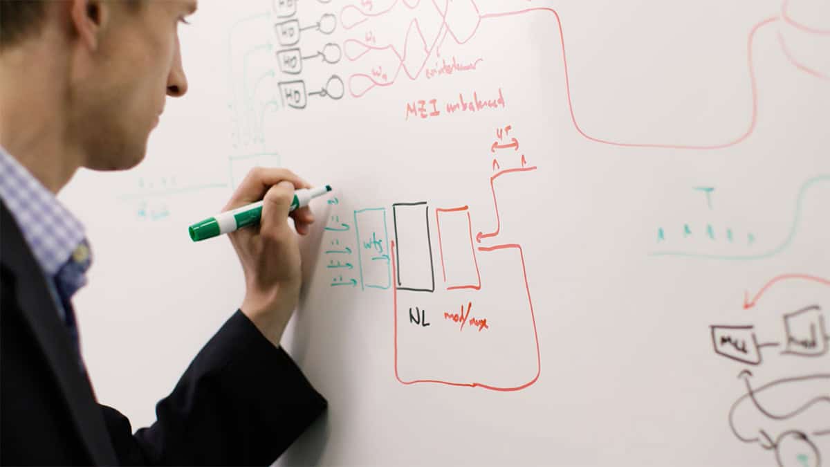
Starting out Ryan Hamerly recently helped launch photonic processor start-up Opticore alongside his academic collaborators. (Courtesy: NTT Research, Inc)

However, the chance to meet and interact with scientists from different areas is still the same. “Science is science, regardless of what institution you’re affiliated with,” he says. “We’re still doing the same things: we do research in a lab, we write up the results, submit them and publish them in journals, and we go to conferences and present our work.”

Hamerly still sees himself as principally a theorist. He spends much of his time writing computer code – occasionally for models that run on a supercomputer but usually for models that can run on his laptop. The rest of his time is focused on writing papers, travelling to present work, responding to reviews or in meetings.

Looking to the future, Hamerly believes that technology will impact research, but that the core elements of a researcher’s role are likely to remain similar for the foreseeable future. “The job of a researcher before the Internet, for example, is not too different from a post-Internet researcher,” he says, pointing to how you still have to communicate research via papers and conferences, and understand the field by reading others’ publications.

“There will definitely be changes in the way you do every one of these things in the next 10 years, especially with AI, but I don’t see any of them becoming optional.”

For young researchers entering the field, Hamerly advises keeping your options open. He did not envisage himself leaving full-time academia and work in an industrial lab, but switched because it offered a better opportunity to pursue the research he wanted to do. “They are both good routes to do research,” he concludes, “but you might find – based on which offers you get – that one is better than another.”

The post From ideas to industry: a theoretical physicist’s journey into Silicon Valley appeared first on Physics World.

  •  

Photonic glasses deliver angle-independent structural colour, including reds

Photonic glasses containing gold-cored, silica-shelled nanoparticles can produce high-purity colours across the visible spectrum. Crucially, the colours are independent of viewing angle. Developed by researchers in Korea, their design avoids the short-wavelength scattering that has prevented the attainment of a true red – and blurred other colours – in previous photonic glasses.

Synthetic materials are usually coloured using pigments, such as those found in dyes or paints. A pigment has a chemical composition that causes it to reflect light at certain wavelengths and absorb light at other wavelengths. Nature, however, makes widespread use of structural colour, whereby the physical structure of a material dictates which wavelengths are reflected and which are absorbed. A familiar example is iridescence, which is responsible for rainbow-like colours on some plants and animals.

Creating colour using structure rather than chemistry has several advantages. One is that there are no chemical chromophores to be bleached by sunlight, so the colour tends to be more durable. Another benefit is that there is no dye to leach if the material comes into contact with water or another solvent.

While structural colour can be created using traditional photonic crystals, these can be tricky to produce controllably. Moreover, a surface that relies on interference effects is inevitably iridescent – which means that its colour changes with the viewing angle.

Short-range order

One solution is colloidal photonic glasses, which are not physically textured but have particles such as silica or polymers dispersed throughout them with short-range order. These can be produced simply by solution processing, and their colour does not vary with viewing angle. The principal problem with these glasses is the attainment of colour purity – especially in the red. The challenge is that the glasses scatter light more effectively at shorter (bluer) wavelengths owing to Rayleigh scattering. This effect makes the sky appear blue and adds unwanted blue light to structural colour.

In the new work, nanophotonics expert Seungwoo Lee of Korea University in Seoul and colleagues synthesized 230 nm core–shell nanoparticles in which silica surrounds a 20 nm gold cluster. This has a plasmonic resonance that absorbs shorter wavelengths. The researchers then dispersed the nanoparticles in ethoxylated trimethylolpropane triacrylate. This is a photocurable resin that has a very similar refractive index as the nanoparticles. The resin was applied to surfaces by painting or solution deposition and then cured under ultraviolet light.

The resulting photonic glass scatters red light randomly, while absorbing shorter wavelengths. Lee stresses that this is different from a traditional paint. “The reflected colour is determined by particle size, spacing, refractive-index contrast, and the degree of structural order, rather than by a molecular chromophore alone,” he says. When the researchers reduced the size of the nanoparticle shells, first to 180 nm and then to 160 nm, they found that they packed more closely together, producing first green and then deep blue colours.

The explanation for the blue scattering is more subtle than for the red: “The gold core is not needed to ‘make’ blue in the same way that a blue dye would,” explains Lee. “However, the gold core can still improve perceived colour purity by reducing broadband diffuse scattering and nonresonant background light.” explains Lee “Without this suppression, silica-only photonic glasses tend to look milky or whitish because many wavelengths are scattered together.”

Durable coatings

The researchers are now exploring several possible extensions of their research. They believe that the work could provide easily applied coatings that are durable as the light scattering comes from within the material structure rather from than a surface pigment.

They also believe it could have anti-counterfeiting properties: “In a normal ink or paint, its colour mainly originates from chemical pigments or dyes,” says Lee; “Our material produces a nanoscale structural signature: a specific reflectance spectrum, bandwidth, angular response, and microstructural arrangement determined by the particle diameter, core–shell geometry, refractive-index matching, volume fraction, and assembly pathway. This gives several possible authentication handles.”

Lee believes that it should be possible to reduce the cost of the material using a metal that is cheaper than gold. However, the precious metal is only 0.022% of the film by weight, so the technology may already be economically viable.

The film is described in Proceedings of the National Academy of Sciences.

“I think it’s really neat,” says materials scientist Aaswath Raman of the University of California, Los Angeles. “The concept of structural colour has been around for a really long time but to me it’s, like, the last steps before we see it out it the real world.”

He says the largest problems he foresees are the simple economics of competing with industrially-optimized paint industry – even if the technology is, in principle, superior. Nevertheless, he says, “of the technologies we see in research this is likely quite a good candidate for commercialization”. The next step, he says, is to actually find a “first use” application – he suspects the aerospace industry, which values ultralight, durable coatings, could be a candidate.

The post Photonic glasses deliver angle-independent structural colour, including reds appeared first on Physics World.

  •  

World’s First Room-Temperature Quantum Material Sorts Light in an Unprecedented Way

Quantum Materials Engineering Concept IllustrationQuantum materials could transform technologies ranging from powerful computers and highly secure communications to advanced energy systems, but one major obstacle has long stood in the way. Most quantum materials reveal their unusual properties only when chilled to temperatures near absolute zero. At room temperature, continual atomic vibrations caused by heat can overpower the fragile [...]
  •  

Topological Jackiw-Rebbi States in Photonic Van der Waals Heterostructures

A new study is turning an elegant quantum idea into a practical platform for light. In research published in Light: Science & Applications, physicists report “topological Jackiw–Rebbi” states engineered inside photonic van der Waals heterostructures—systems built by stacking atomically thin materials with precisely tailored interfaces. The result is a photonic phenomenon that echoes how particles can be trapped at boundaries where the rules of their governing equations change.

The work builds on the classic Jackiw–Rebbi mechanism, originally proposed for relativistic particles. In those models, a localized mode appears when a mass term flips sign, effectively creating a domain wall. The authors translate this concept into optics by designing photonic structures where an effective “mass” characterizing light propagation changes across an interface.

What makes the platform especially compelling is the van der Waals architecture. Unlike conventional fabrication routes that can introduce disorder, the layered nature of these materials enables sharp, controllable boundaries and tunable photonic band structures. By adjusting the stacking and interlayer optical responses, the researchers create conditions in which topological modes become robust against typical imperfections.

The study emphasizes that these states are not merely conventional guided resonances. Instead, they are tied to topology: the light modes are associated with an invariant property of the band structure. As a consequence, the Jackiw–Rebbi-like photonic states are expected to persist even when the system’s details vary, so long as the relevant symmetry and band configuration remain intact.

Topological protection is more than a slogan. In photonics, it can translate into reduced sensitivity to fabrication tolerances and a pathway toward devices that rely on stable boundary transport. The paper therefore positions these localized states as building blocks for future optical components that route signals along designed interfaces.

The authors demonstrate the concept theoretically and connect it to experimental observables by focusing on how the interface should host modes localized near the domain wall region. Such localization is a hallmark of the Jackiw–Rebbi scenario, now realized in a controllable, designer photonic environment.

Beyond fundamental interest, the approach could influence the design of reconfigurable photonic circuits. Because van der Waals stacks can be combined and adjusted, the same topology-driven logic may be extended to new material systems, wavelengths, and device geometries.

Overall, the report signals a broader trend: using topological field-theory ideas to engineer light–matter behavior in atomically precise platforms, potentially enabling the next generation of robust, interface-based photonic technologies.

Subject of Research: Topological photonic states (Jackiw–Rebbi) in van der Waals heterostructures.

Article Title: Topological Jackiw-Rebbi states in photonic Van der Waals heterostructures.

Article References: Randerson, S.A., Bouteyre, P., Hu, X. et al. Light Sci Appl 15, 323 (2026). https://doi.org/10.1038/s41377-026-02392-5

Image Credits: AI Generated

DOI: 10.1038/s41377-026-02392-5

Keywords:

  •  

New optical chip design controls light speed in real time, simulations suggest

Seoul National University College of Engineering announced that a joint research team led by Professor Namkyoo Park and Professor Sunkyu Yu of the Department of Electrical and Computer Engineering at SNU, in collaboration with Professor Xianji Piao of the School of Electrical and Computer Engineering at the University of Seoul, has developed a photonic integrated circuit that can slow light on demand.

  •  

Quantum teleportation could reduce photon loss in long-distance communications

Quantum technologies, which leverage the principles of quantum mechanics, have been found to outperform their classical counterparts on specific tasks. Among other things, past studies have highlighted the potential of quantum systems that can enable long-distance communication, using photons (i.e., particles of light) to carry quantum information.

  •  

Turning Quantum Potential into Reality

In a groundbreaking stride toward the future of quantum technology, researchers have unlocked a new mechanism to control quantum emitters embedded in hexagonal boron nitride (hBN), a layered two-dimensional material. This breakthrough could serve as a critical leap forward in integrating quantum emitters into practical devices, bringing quantum computing, secure quantum communications, and ultra-sensitive quantum sensors closer to reality. This promising development emerged from meticulous experimental studies demonstrating the ability to reversibly tune the color and wavelength of light emitted by quantum defects in hBN simply by twisting its atomic layers.

Quantum emitters are nanoscopic sources of light that emit photons with quantum characteristics, pivotal for next-generation technologies reliant on quantum information processing. However, a formidable challenge in utilizing these emitters has been the difficulty in precisely controlling their optical properties post-fabrication. Dr. Angus Gale, the lead scientist behind this research, elucidated how their work provides an innovative “lever” by exploiting the intrinsic layered nature of hBN to adjust the quantum emission properties dynamically. Unlike traditional solid-state hosts such as diamond or silicon carbide, whose structures are rigid and three-dimensional, hBN’s atomically thin layers can be mechanically manipulated, lending itself to an unprecedented degree of tunability.

The team’s experiments demonstrated that by picking up, stacking, twisting, and restacking these ultra-thin hBN slices at varied angles, they could modulate the quantum emitters’ light emission dramatically. These shifts in wavelength were not minor perturbations but substantial changes far exceeding what has been typically achievable in similar solid-state quantum systems. This finding challenges the traditional paradigm which often seeks to stabilize quantum defect behavior within rigid host materials. Instead, the researchers embraced the inherent flexibility and twistability of hBN to realize a new class of quantum control.

Professor Igor Aharonovich, the supervising author, emphasized the broader implications of this twist-controlled modulation approach. He noted that coupling two-dimensional materials at specific twist angles opens up an entirely fresh set of physical phenomena that were previously inaccessible. By assembling layers with precision angular misalignment, new quantum states can emerge, potentially transforming the landscape of material engineering for quantum applications. This strategic layering and twisting, known as “twistronics,” has already inspired revolutionary advances in graphene-based systems, yet this study extends the concept into the realm of quantum emitters embedded in hBN.

One key advantage of using hBN is that its layered crystal structure allows researchers to systematically alter the interaction between layers, effectively tuning the electronic environment surrounding the defects responsible for quantum light emission. As Dr. Gale metaphorically illustrated, far from being a solid block, hBN behaves more like a stack of cheese slices. Just as peeling and recombining slices of cheese can change how flavors intermingle, twisting hBN slices changes the interaction between atomic planes, which in turn alters quantum emitter characteristics. This mechanical engineering at the nanoscale provides a versatile platform for on-demand tuning of quantum light sources.

This technology breakthrough is fundamentally experimental but holds widespread implications. Adjustable quantum emitters could accelerate the development of quantum computing hardware, where precise photon control is essential for encoding and manipulating qubits. Similarly, secure quantum communication protocols rely on tailored quantum light sources to guarantee the generation and distribution of entangled photons immune to interception. Moreover, quantum sensing that exploits the extreme sensitivity of quantum states to environmental changes stands to benefit significantly from tunable quantum emitters, pushing the boundaries of detection limits in fields ranging from medicine to navigation.

Another remarkable facet of the research is the ability to repeatedly pick up, twist, and restack hBN layers without degrading the quantum emitter properties. This reversibility enables iterative fine-tuning of device characteristics and might yield adaptable quantum systems reconfigurable post-production, a feature highly desirable from a technological deployment perspective. This contrasts sharply with permanent structural modifications used in conventional quantum emitter fabrication, which restrict adjustable control and device flexibility.

The team’s methodology involved sophisticated nanofabrication techniques and high-resolution optical spectroscopy to probe the quantum emitters’ response to twist-induced modifications. By correlating the angular misalignment with spectral shifts in emitted light, they constructed a detailed understanding of the underlying physics governing emission control. These insights provide a blueprint for engineering tailored quantum emitters with bespoke characteristics suitable for specific applications.

The research findings have been detailed in a paper published in the eminent journal Science Advances, signaling the scientific community’s enthusiasm for the potential unlocked by twistable quantum systems. Importantly, the authors have declared no competing interests, affirming the independent and foundational nature of this inquiry. Funded by the Australian Research Council and the Air Force Office of Scientific Research, the work highlights the vibrant collaboration between academic institutions and funding bodies committed to propelling quantum technologies.

This discovery heralds a new era in quantum material science, where layered two-dimensional crystals are no longer passive hosts but active tunable platforms. By harnessing the mechanical and electronic versatility of materials like hBN, researchers are gradually unlocking complex quantum phenomena with precision control previously deemed unachievable. The implications extend well beyond fundamental research, marking exciting progress toward quantum devices that could redefine computational power, information security, and sensory precision globally.

In summary, the twist-controlled modulation of quantum emitters in hexagonal boron nitride exemplifies the convergence of cutting-edge experimental physics and materials science innovation. By capitalizing on the unique layered architecture of hBN and the emerging discipline of twistronics, this research pioneers functional tunability in quantum light sources. As the scientific community continues to develop and refine these approaches, we edge closer to the practical implementation of quantum technologies that promise profound societal and technological transformation.


Subject of Research: Not applicable

Article Title: Twist-controlled modulation of quantum emitters in hexagonal boron nitride

News Publication Date: 19-Jun-2026

Web References: 10.1126/sciadv.aec0101

References:

  • Gale, A., Aharonovich, I., et al. Twist-controlled modulation of quantum emitters in hexagonal boron nitride. Science Advances. 19 June 2026.

Keywords:
Quantum mechanics, Hexagonal boron nitride, Two-dimensional materials, Quantum emitters, Twistronics, Quantum light sources, Quantum computing, Quantum communication, Quantum sensing, Layered materials, Nanofabrication, Photonic modulation

  •  

Emerging Frontiers in Photonic Computing: Revolutionizing Medical Diagnosis with Photonic AI

A groundbreaking advancement in photonic technology promises to redefine the landscape of medical artificial intelligence (AI) diagnostics, as a research consortium led by Professor Han Zhang at Shenzhen University has unveiled a novel all-fiber photonic AI platform utilizing black phosphorus (BP)-based tunable modulators. This innovative approach, which hinges on photon-based computing, surmounts the intrinsic constraints posed by traditional electronic processors, delivering unprecedented energy efficiency and ultrafast performance crucial for real-time clinical decision-making.

The prevailing paradigm in medical AI, deeply reliant on electronic architectures such as GPUs, faces severe limitations related to energy consumption, heat dissipation, and processing latency. These factors collectively impede the integration of AI into time-sensitive diagnostic workflows and exacerbate systemic carbon footprints. Photonic computing, with its reliance on photons rather than electrons, offers dramatically accelerated data transmission speeds and parallelism through wavelength multiplexing, alongside near-zero heat generation. Until now, however, the practical implementation of photonic AI had been hampered by the bulkiness, inefficiency, and fabrication challenges synonymous with conventional optical modulators.

Professor Zhang’s team has ingeniously engineered an atomically thin van der Waals heterostructure by stacking black phosphorus and molybdenum disulfide (MoS2), leveraging the extraordinary optoelectronic properties of these 2D materials. This heterostructure is meticulously integrated onto a microfiber knot resonator (MKR), an ultra-fine looped optical fiber with a diameter narrower than a human hair. This configuration significantly intensifies the interaction between light and material, enabling modulation of the refractive index with minimal applied voltage, which shifts the light’s wavelength to encode computational information with remarkable precision and energy economy.

The fabrication process commences with mechanical exfoliation to obtain pristine BP/MoS2 bilayers, followed by a dry transfer technique to position these heterostructures onto the MKR. The MKR’s torsional geometry enhances evanescent field coupling, ensuring that the optical mode overlaps maximally with the active layered materials. To broaden the modulator’s linear response and suppress nonlinear distortions, the researchers incorporated a Ring-Assisted Mach–Zehnder Interferometer (RAMZI) design. This integration extends the operational voltage range, ensuring fidelity and robustness essential for medical-grade AI computations.

The team transcended single-device innovation by architecting a full all-fiber photonic neural network (PNN). By deploying two RAMZI modulators in tandem with a highly sensitive photoreceiver within a sophisticated time-division multiplexing schema, they realized a closed-loop, coherent computing unit capable of executing neural network operations entirely in the optical domain. This milestone substantiates the transition of photonic neural networks from theoretical constructs to viable, deployable platforms for clinical diagnostics.

Clinical performance validation was conducted in collaboration with esteemed hospitals. The PNN demonstrated expert-level diagnostic accuracy in two stringent medical tasks: detecting retinal detachment from B-scan ultrasound imagery and diagnosing hepatocellular carcinoma (HCC) using multiphase liver computed tomography (CT) scans. Diagnostic accuracy and specificity metrics paralleled those of seasoned radiologists, underscoring the system’s potential for integration into frontline healthcare.

Beyond accuracy, the photonic system showcased transformative efficiency advantages. While a conventional NVIDIA A100 GPU requires approximately 85 milliseconds to process a liver CT study, the photonic platform accomplished the same in a mere 0.8 milliseconds. Additionally, the energy expenditure per operation plummeted to an astonishing 0.608 femtojoules, a staggering 246-fold decrease compared to electronic counterparts consuming 150 femtojoules. This synergy of speed and efficiency paves the way for deploying AI diagnostics in resource-constrained or mobile medical environments like rural clinics and ambulances, dramatically expanding access to critical health services.

The system’s environmental implications cannot be overstated. Conventional AI’s sizable energy footprint contributes appreciably to healthcare’s carbon emissions. The BP/MoS2-based photonic platform fundamentally disrupts this model by combining ultrafast processing with near-negligible thermal dissipation, forging a sustainable pathway for green AI implementations in medicine. This breakthrough aligns with expanding global commitments to environmentally responsible technologies without sacrificing computational power.

Acknowledging the infancy of current implementations, the authors outline avenues for scaling. Presently limited to a single processing layer realized through two modulators, the system’s complexity and image resolution capacity necessitate expansion. A promising strategy involves wavelength-division multiplexing (WDM), exploiting the device’s ∼30 nm bandwidth resonances to channel up to 40 distinct wavelengths. This parallelism would amplify computational density approximately 40-fold while maintaining the existing clock rate, facilitating thousands of multiplications per network layer—an enhancement critical to tackling high-dimensional medical image data.

Device longevity and stability pose additional challenges, given the sensitivity of BP to environmental degradation. While the MoS2 layer affords interim encapsulation, the team plans industrial collaboration to pioneer large-scale protective coatings via atomic layer deposition of Al2O3 and scalable chemical vapor deposition processes. These advancements will bolster device durability, uniformity, and manufacturability, accelerating clinical adoption and commercial viability.

The study also signifies the maturation of fiber-based photonic neural networks into practical diagnostic platforms rather than experimental novelties. Optical fibers’ inherently low transmission loss (<0.2 dB/km), synergized with the modulator’s efficient 0.25 V·cm electro-optic response and expanded linear range, addresses critical bottlenecks impeding prior photonic computing endeavors. Consequently, the technology promises to empower future applications in drug discovery, genomics, and real-time clinical imaging with unmatched energy footprints.

The pioneering work led by Professor Han Zhang not only foregrounds interdisciplinary collaboration across physics, materials science, and biomedicine but also sets a precedent for industry-academia partnerships catalyzing the commercialization of ultrafast photonic devices poised to transform healthcare AI. As research progresses towards integrated multi-layer architectures and industrial encapsulation, the healthcare sector stands on the cusp of embracing a new generation of diagnostic tools that are faster, greener, and broadly accessible.

This heralds a paradigm shift where medical AI transcends the limitations inherent to electronic systems, embracing photon-driven computing as a sustainable, high-performance alternative that aligns with the twin imperatives of clinical excellence and environmental stewardship.


Subject of Research: People

Article Title: Tunable phosphorene modulators – accelerating medical diagnosis with ultra-efficient photonic platforms

News Publication Date: 28-May-2026

References:
Zhang, H., Liu, Y., Wang, H., Zhu, H., et al. (2026). Tunable phosphorene modulators – accelerating medical diagnosis with ultra-efficient photonic platforms. Opto-Electronic Advances. DOI: 10.29026/oea.2026.250332

Image Credits: Professor Han Zhang of Shenzhen University

Keywords: photonic computing, black phosphorus, molybdenum disulfide, van der Waals heterostructure, microfiber knot resonator, electro-optic modulator, photonic neural network, medical imaging AI, energy efficiency, wavelength-division multiplexing, ultrafast diagnostics, sustainable healthcare

  •  

This AI Learned the Laws of Physics and Could Accelerate Quantum Computing Breakthroughs

Physics Inspired AI Super BrainResearchers in Sweden have developed a machine-learning approach that embeds the laws of physics directly into neural networks. A new study from Chalmers University of Technology in Sweden shows that machine learning can become far more efficient when it starts with a built-in understanding of the laws of physics. Researchers found that giving an AI [...]
  •  

This Strange Crystal Bends Light Like Nothing Else in Nature

Guiding Light MoOCl2This record-breaking crystal can transform from mirror-like to glass-like, opening the door to tiny optical chips, AR displays, and smart contact lenses. Creating truly “invisible” wearable technology such as smart contact lenses and ultrathin augmented reality glasses will require a radical rethink of how optical devices are built. Instead of relying on conventional bulky components, [...]
  •  

This Quantum Detector Boosts Terahertz Sensitivity by 20 Times

Quantum Metasurface Based Photoelectric Tunable Step Terahertz DetectorA quantum metasurface breakthrough boosts terahertz detection by 20 times, bringing practical THz technology a step closer. Detecting light and radiation is essential across the electromagnetic spectrum, but some regions remain difficult to work with. One of the biggest challenges involves terahertz (THz) radiation, which sits between microwaves and infrared light. Existing detectors for these [...]
  •  

The Laser That Once Filled a Lab Now Fits on a Tiny Chip

Chip Based Ultrafast LaserScientists have finally packed a laboratory-class ultrafast laser onto a tiny photonic chip. Ultrafast lasers generate bursts of light that last only a few hundred femtoseconds, each one just a quadrillionth of a second long. These extremely short pulses are used in a wide range of technologies, including precision manufacturing, eye surgery, and optical frequency [...]
  •  

MIT Engineers Solve a Major Lidar Problem That Has Stumped Researchers for Years

Array of Integrated Antennas Minimizing Unwanted CrosstalkA new MIT-designed lidar chip uses specially engineered antennas to reduce interference and widen the sensor’s field of view. From self-driving cars navigating busy streets to drones surveying disaster zones, lidar has become one of the most important technologies for helping machines perceive the world in three dimensions. By sending out rapid pulses of infrared [...]
  •  
❌