Coway employees and Gyeongil Elementary School students plant vegetation in the third Coway Ecological Forest. (Photo: Coway)
Coway employees and Gyeongil Elementary School students plant vegetation in the third Coway Ecological Forest. (Photo: Coway)
Coway has created an ecological forest featuring endangered and rare plants at Gyeongil Elementary School in Seongdong District, Seoul. The site will serve as an ecological learning space where students can observe plants and other living organisms.
Coway said on Sept. 16 that it created the third Coway Ecological Forest, covering about 365 square meters, on the school's grounds.
Coway planted 1,195 plants from 25 species, including endangered and nationally protected species such as Pseudolysimachion pusanensis, Hosta yingeri and Aster koraiensis. Coway employee volunteers and Gyeongil Elementary School students participated in the planting.
Environmental social enterprise Tree Planet and the Landscape Architecture Design Lab at the University of Seoul were responsible for the forest's design and construction. The ecological forest incorporates results from research collaboration between the two organizations.
Environmental education for students was also conducted after the forest was completed. Students observed the forest and completed ecological forest checklists. Coway selected 13 students as ecological forest gardeners and provided them with garden maintenance kits.
Coway operates an ecological forest program that plants endangered and rare species in South Korea designated by the International Union for Conservation of Nature (IUCN) and the Korea Forest Service, as well as plants endemic to the Korean Peninsula. The company created its first ecological forest in an outdoor space at its headquarters in 2024 and its second at Banghwa Elementary School in Seoul last year.
Coway also operates environmental social contribution programs including Clean School Classroom Forest, which provides air-purifying plants to elementary schools; river plogging to collect waste along waterways; and the throwing of effective microorganism (EM) mud balls to improve water quality.
Novathermo CEO Kim Hyung-chul. (Photo: Novathermo)
Novathermo CEO Kim Hyung-chul. (Photo: Novathermo)
Novathermo, a thermal management materials startup, is focusing its resources on thermal materials for artificial intelligence (AI) semiconductors and automotive electronics. Following the commercialization of a high-thermal-conductivity material for printed circuit boards (PCBs), the company has added silicone thermal pads to its product lineup. It aims to reach 36 billion won in sales by 2030.
Kim Hyung-chul, CEO of Novathermo, said on Sept. 16 that PCB thermal materials require significant time for final validation because they undergo multiple processes while still in a semi-finished state, while thermal interface material (TIM) silicone pads can be evaluated by customers in a form close to the finished product after production and before shipment.
"It is significant because this is our first commercial product line that expands our thermal management technology into the TIM market, where demand is substantial," Kim said.
Novathermo develops and produces new polymer-based thermal materials using carbon nanotubes (CNTs). Its main products are designed to rapidly transfer heat generated by semiconductors and automotive electronic components while maintaining electrical insulation. The company is developing thermal materials for PCBs, semiconductor packaging and power electronics.
Its core technology involves uniformly dispersing highly thermally conductive materials such as CNTs and alumina within polymers. Novathermo uses a high-shear mixing process to reduce material agglomeration and create pathways for heat transfer. The technology is designed to improve thermal performance while maintaining electrical insulation and mechanical strength.
Its flagship product is Aqua, a high-thermal-conductivity material for PCBs. PCBs are substrates that connect semiconductors and other electronic components. Aqua enables the PCB material itself to conduct heat efficiently, allowing heat generated by chips to dissipate through the substrate as well.
Heat generated by semiconductors is typically removed through heat sinks or cooling systems positioned above the chip. Aqua adds another heat-transfer path through the underside of the substrate. In Novathermo's own tests, replacing only the material with Aqua while keeping the substrate thickness and component configuration unchanged reduced chip temperatures by as much as 30% and substrate temperatures by 20%. The product was commercialized in November last year.
The material achieves thermal conductivity of about 2 watts per meter-kelvin (W/m·K) on mass-production equipment. Novathermo has achieved up to 3.3 W/m·K at the laboratory stage. Thermal conductivity measures how effectively a material transfers heat, with higher values indicating faster heat transfer.
Novathermo has also completed customer validation for automotive components. In a comparison of identical circuits using different PCB materials in an automotive lidar module, Aqua lowered the temperature of the transmitter (Tx) chip by more than 10 degrees Celsius compared with the conventional material. The company said that exceeded the customer's initial target of a 4-degree reduction.
The company is also conducting proof-of-concept (PoC) projects with global companies. PoC involves applying the material directly to a customer's product to determine whether it meets required performance specifications. Successful validation could lead to additional reliability testing and discussions on mass-production supply.
Novathermo has also introduced FLEXURE, a silicone thermal pad brand. It has established mass-production capabilities for products with thermal conductivity ratings of 3, 5 and 8 W/m·K. The company has also completed prototype design for a high-performance 12 W/m·K product line.
FLEXURE is placed between a semiconductor chip and a heat sink. Microscopic gaps form between the surfaces of the chip and heat sink, and air trapped in those spaces can impede heat transfer. The silicone pad fills the gaps, transferring heat generated by the chip to the heat sink.
A key challenge in product development is achieving both thermal performance and suitable physical properties. Adding more filler to increase thermal conductivity can make a pad harder or more prone to tearing while reducing its ability to conform to component surfaces. Novathermo adjusted the filler composition, silicone structure, cross-linking and molding processes to improve thermal conductivity, dimensional stability and surface conformity.
Novathermo plans to expand its customer base in semiconductor packaging, power electronics and automotive electronics, centered on its high-thermal-conductivity PCB materials and silicone TIM pads. Its current mass-production yield is about 70%.
The company also plans to expand production capacity. Monthly output is targeted to rise from 10,000 panels this year to 1.2 million panels in 2030. Over the same period, the number of key customers is expected to increase from three to 25, while exports are targeted to rise from 10% to 55% of sales. Novathermo aims for 36 billion won in revenue by 2030.
"Customers requesting samples are focusing not only on thermal performance but also on the pads' ability to resist tearing and maintain surface conformity even under high-hardness conditions," Kim said. "We will improve product quality and mass-production reliability to help localize high-performance thermal materials that are heavily dependent on overseas suppliers and stabilize the supply chain."
An OLEDoS product displayed by Samsung Display at AWE USA 2025. (Photo: Samsung Display)
An OLEDoS product displayed by Samsung Display at AWE USA 2025. (Photo: Samsung Display)
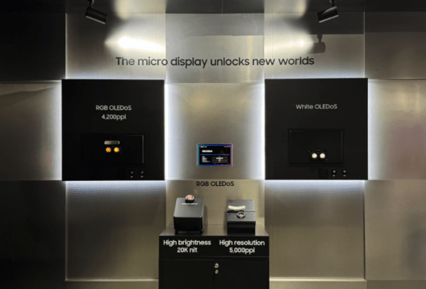
Samsung Display plans to invest about 300 billion won to mass-produce red, green and blue (RGB) OLED-on-Silicon (OLEDoS) displays. Sunic System will supply the deposition equipment, which accounts for about half of the investment.
According to industry sources on Sept. 15, Samsung Display will hold an investment review committee meeting this month to finalize investment in 12-inch RGB OLEDoS mass production. The line will have capacity to process 3,000 wafers per month, with the investment estimated by the industry at about 300 billion won. The location has not been confirmed, but the line is likely to be built at the A2 plant, which already has a 12-inch white OLEDoS (WOLEDoS) line.
Samsung Display evaluated 12-inch RGB OLEDoS deposition systems from Sunic System and Japan’s Canon Tokki earlier this year. After comparing equipment performance and supply experience, the company selected Sunic System.
The deposition equipment to be supplied by Sunic System is expected to cost about 150 billion won, roughly three times the 40 billion won to 50 billion won price of conventional OLEDoS deposition equipment. The higher cost reflects the need for significantly tighter vibration control and mask-to-wafer alignment precision to form RGB emissive layers on individual subpixels.
The remainder of the capital expenditure will go toward front- and back-end equipment for encapsulation, inspection, cleaning and material handling. Actual spending may vary depending on equipment specifications and the extent to which existing infrastructure can be used.
Equipment orders are expected in the fourth quarter. Following approval of the investment, Samsung Display is expected to finalize detailed equipment specifications, delivery schedules and acceptance conditions before signing purchase contracts.
Samsung Display is considering bringing in equipment in 2027 and starting mass production of RGB OLEDoS in 2028. Equipment manufacturing, installation, commissioning and process stabilization are expected to take more than a year.
OLEDoS is a microdisplay that forms OLED emissive layers on a silicon wafer. It is divided into white OLEDoS and RGB OLEDoS depending on how colors are produced.
WOLEDoS uses color filters over a white organic light-emitting diode (OLED) emissive layer to produce RGB colors. Because organic materials do not need to be separately deposited for each subpixel, the deposition process and mask-alignment requirements are less demanding. Mass-production technology and supply chains are already established, and WOLEDoS is used in commercial extended reality (XR) devices including Apple Vision Pro.
Some light, however, is lost as white light passes through the color filters. Increasing screen brightness requires more power, which can result in disadvantages in heat generation and battery life.
RGB OLEDoS directly deposits red, green and blue emissive layers on individual subpixels. Eliminating color filters reduces light loss and offers advantages in brightness, luminous efficiency and color reproduction.
RGB emissive layers can be formed using either mask-based or maskless methods. Samsung Display is expected to use a mask-based deposition process. Forming emissive layers on subpixels measuring only a few micrometers requires repeated, highly precise alignment of the mask and wafer during deposition.
A tandem structure requires multiple emissive layers to be stacked, increasing the number of deposition chambers and transfer systems. Controlling mask sagging, thermal deformation, positioning errors and deposition-thickness variations across an entire 12-inch wafer also presents technical challenges.
Samsung Display acquired US microdisplay company eMagin in 2023 and has since been developing RGB OLEDoS technology. The yield of eMagin’s 8-inch RGB OLEDoS process is known to be about 20%.
Expanding wafer size from 8 inches to 12 inches makes controlling deposition uniformity and alignment errors more difficult. Samsung Display’s actual mass-production schedule and output will depend on its ability to secure sufficient yields on the 12-inch process.
“RGB OLEDoS has advantages in brightness and efficiency, but mass production on 12-inch wafers has yet to be proven,” an industry official said. “How quickly yields can be stabilized after the equipment is installed will determine the timing of commercialization.”
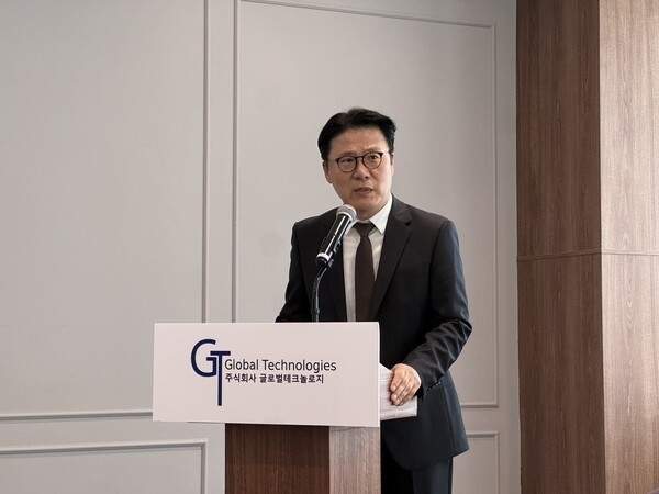
Kim Min-sun, CEO of Global Technologies, speaks about the company at a press briefing at the CCMM Building in Yeouido, Seoul, on Sept. 10. (Photo: THE ELEC)
Kim Min-sun, CEO of Global Technologies, speaks about the company at a press briefing at the CCMM Building in Yeouido, Seoul, on Sept. 10. (Photo: THE ELEC)
Global Technologies aims to generate 169.5 billion won in revenue by 2029 by expanding its light-emitting diode (LED) driver IC, transparent display, micro LED and automotive system semiconductor businesses.
Kim Min-sun, chief executive officer of Global Technologies, said at a press briefing at the CCMM Building in Yeouido, Seoul, on Sept. 10 that the company plans to expand its LED driver IC technology from TVs to monitors and automobiles, while developing micro LED and automotive system semiconductors as new growth engines.
Global Technologies is a fabless chipmaker that designs LED driver ICs (LDIs) controlling the current and brightness of backlight LEDs. The TV market currently accounts for about 70% of its revenue. The company secured a purchase order from a Taiwanese display customer in July. It plans to begin mass production of monitor LDIs in December and is developing automotive products with a target of mass production in the second half of next year.
The company is also developing a red-green-blue (RGB) backlight module combining driver ICs, LED packages and lenses. The key technology is time-division driving, which alternately controls three light sources through a single output channel. Conventional designs use a separate channel for each light source. By sharing the control circuitry, the technology can reduce the number of driver ICs required to as little as one-third of the conventional level.
Global Technologies plans to use the reduced chip count to counter price competition from Chinese suppliers. TV makers can lower overall component costs without cutting the price of individual chips. The company aims to improve profitability by charging higher prices for chips incorporating the technology while increasing shipment volumes as customers expand their adoption of RGB LED models. A TV-set customer will evaluate the technology this month, with mass production targeted for early next year.
In transparent LED displays, the company is targeting commercial signage and automotive glass. The products combine driver ICs with ultra-small LED packages, allowing users to see through the display. Global Technologies has supplied commercial products to customers including Yangju City Hall in Gyeonggi Province and is developing products for vehicle rear windows and roofs.
In micro LEDs, the company is jointly developing pixel driver ICs, packages and modules. A 24-pixel driver IC for TVs is targeted for mass production early next year. The company is also developing modules for automotive center information displays (CIDs). It invested 5 billion won to establish a pilot line in Pyeongtaek for prototype production and process validation.
Global Technologies is developing lighting and communications products for its automotive system semiconductor business. It operates a joint research center with an automotive parts supplier and is developing about 10 products. Its smart ambient lighting (SAL) IC, which controls vehicle interior lighting, has secured an initial order for 3 million units, with deliveries scheduled to begin early next year. The company also plans to commercialize controller area network (CAN) communication chips used to exchange data among vehicle electronic systems.
The company posted first-half revenue of 28.8 billion won and operating profit of 1.155 billion won this year. It generated revenue equivalent to 97% of last year's full-year total in the first half and returned to an operating profit. Global Technologies plans to increase revenue from mass-produced products and raise its operating margin from a target of 7.7% this year to 21.8% in 2029.
Global Technologies is scheduled to list on the KOSDAQ on Sept. 29. It is offering 4 million shares at an indicative price range of 13,000 won to 15,000 won each, for an offering size of 52 billion won to 60 billion won. The company is conducting bookbuilding for institutional investors through Sept. 11 and will accept retail subscriptions on Sept. 16 and 17. Korea Investment & Securities is the lead underwriter.
The company plans to invest a combined 78.7 billion won through 2029 using IPO proceeds, operating cash flow and government funding. Of the total, 23.5 billion won will be allocated to research and development, 7.7 billion won to facility expansion and 47.5 billion won to working capital, including securing foundry capacity.
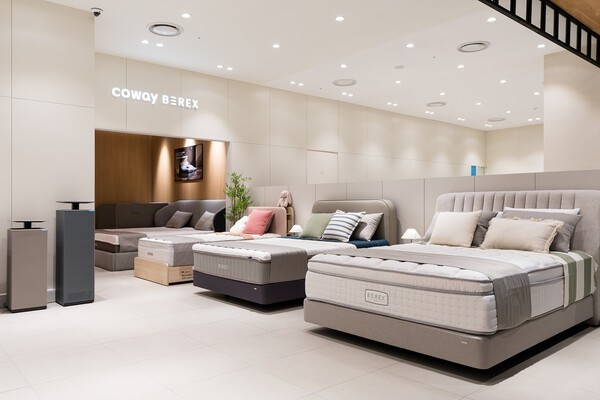
Coway has opened its first directly operated Coway Gallery store in Ansan, Gyeonggi Province.
The company said it opened the Coway Gallery Lotte Ansan store on Sept. 10 on the third floor of the new building at Lotte Department Store’s Ansan branch. The store serves as a showroom and retail space where customers can experience Coway products.
Located in the department store’s living section alongside premium mattress and home-living brands, the store allows customers to try major Coway products, including those from its BEREX sleep and healing care brand.
The store includes a private experience zone where customers can try major sleep-tech products such as the BEREX R7 Stretching Motion Bed and reclining massage set.
Specialist managers are available to provide product demonstrations and consultations. Staff certified as sleep environment consultants offer personalized sleep-care advice based on customers’ sleep patterns, body types and home environments.
Customers can visit the Coway Gallery Lotte Ansan store without advance reservations. Reservations can also be made through Coway.com.
Coway opened 10 new Coway Gallery stores in the first half of this year, including directly operated locations in Suncheon and Pohang. The company plans to expand its offline retail network based on regional commercial conditions and customer demand.
Apple CEO John Ternus introduces the company’s new products. (Photo: Apple)
Apple CEO John Ternus introduces the company’s new products. (Photo: Apple)
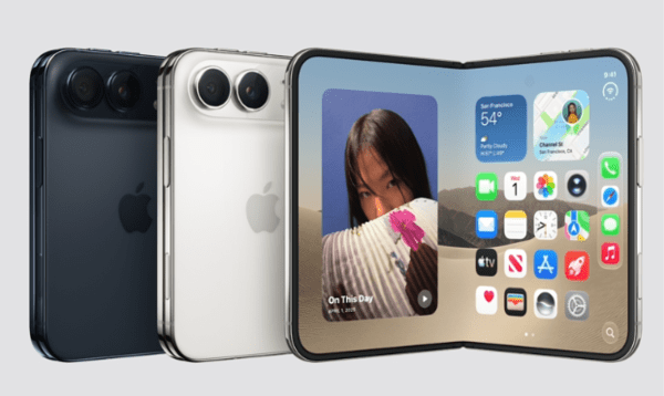
Apple unveiled its first foldable smartphone, the iPhone Duo. The company also introduced a variable aperture for the first time on the iPhone 18 Pro and Pro Max, while improving computing performance and thermal management.
Apple unveiled the iPhone 18 Pro, Pro Max and iPhone Duo at a product event on Sept. 10. The Pro models will go on sale Sept. 18, followed by the Duo on Oct. 23. Prices start at $1,199 for the iPhone 18 Pro, $1,299 for the Pro Max and $1,999 for the iPhone Duo.
Apple did not announce the countries where the iPhone Duo will initially be available.
“The iPhone Duo, iPhone 18 Pro and Pro Max are designed to serve as intelligent personal hubs for users,” Apple Chief Executive Officer John Ternus said. “We put powerful performance and features at the center of the experiences users value most.”
Apple’s first foldable smartphone, the iPhone Duo. (Photo: Apple)
The biggest change is the introduction of a foldable form factor. The iPhone Duo has a 7.6-inch inner display and a 5.4-inch outer display. The inner screen offers 50% more display area than the iPhone 18 Pro Max and 80% more than the Pro. Users can operate the device with one hand when folded and use the larger screen for multiple tasks when unfolded.
Apple also changed how iOS 27 works to take advantage of the larger display. Users can run two apps side by side or open two windows of the same app simultaneously, such as reading an email while viewing a document or comparing two webpages. An app running on the outer display continues on the inner screen when the device is unfolded, while content and controls adjust depending on the folding angle.
The iPhone also supports Apple Pencil for the first time. Starting later this year, the USB-C Apple Pencil can be used on both the inner and outer displays, bringing handwriting, drawing and document annotation features previously centered on the iPad to the iPhone.
Apple also detailed measures to improve crease visibility and surface durability. High-strength glass is placed above and below the organic light-emitting diode (OLED) panel, while a viscoelastic adhesive allows individual layers to move when folded to reduce deformation. A nano-texture surface treatment reduces reflections and glare, making the crease less visible.
The hinge consists of more than 100 precision components. A lower titanium plate and carbon-fiber support plate reinforce the display. During manufacturing, Apple uses a confocal laser to measure the surface profile of each device and applies thin photopolymer layers to correct residual unevenness.
The inner display uses an under-display camera for the first time on an iPhone, reducing the area that obstructs content. The device uses Touch ID integrated into the side button for unlocking. Its exterior is made from Grade 5 titanium and supports IP68 water and dust resistance.
The two displays can also be used for photography. Users can take selfies with the 48-megapixel rear camera while framing shots on the outer display. A preview feature lets subjects see themselves on the outer screen while being photographed.
The iPhone Duo is powered by the A20 Pro and Apple’s C2 modem. A vapor chamber boosts sustained performance by as much as 35% compared with the iPhone 17 Pro. The device manages two battery cells as a single system and provides up to 31 hours of video playback using the inner display and 44 hours using the outer display.
Storage ranges from 256 gigabytes to 2 terabytes. The device will be available in Star White and Night Sky, with preorders beginning Oct. 16.
The iPhone 18 Pro. (Photo: Apple)
The iPhone 18 Pro and Pro Max focus on improvements to photography and sustained performance. The key camera change is a variable aperture introduced for the first time on the 48-megapixel main camera. Unlike a fixed aperture, six polymer-composite blades move to control the amount of light entering the lens.
The variable aperture adjusts both light intake and depth of field depending on shooting conditions. It opens wider in dark environments to capture more light and narrows when users want multiple subjects in focus. Apple said it captures as much as 50% more light in dark conditions. Users can also manually select from four aperture settings.
Apple also added the ability to apply cinematic effects to standard video after recording. For photos, Apple Reference Image signs sensor data at capture and stores an unalterable image alongside the edited version to strengthen original-image verification.
The Pro models use the A20 Pro processor built on a 2-nanometer process. It includes a six-core central processing unit (CPU), seven-core graphics processing unit (GPU) and dual Neural Engines with a combined 32 cores. High-performance CPU core performance improves by as much as 20%, while GPU performance increases by as much as 40%.
Apple also redesigned thermal management. The chip and memory are positioned side by side to transfer heat directly from the chip to the vapor chamber, which is three times larger than the one in the iPhone 17 Pro. The design is intended to reduce performance degradation during prolonged gaming and artificial intelligence workloads. Sustained performance improves by as much as 40% from the previous generation.
Video playback reaches as much as 36 hours on the Pro and 45 hours on the Pro Max for eSIM-only models. The Pro now provides battery life comparable to the previous Pro Max. The battery can be charged to 50% in about 15 minutes.
The Pro models will be available in Deep Black, Silver, Glacier and Burgundy, with preorders starting Sept. 12.
Apple is also bringing Siri AI that uses personal context to all three models. It can respond to requests and perform tasks in apps using information from emails, messages, the screen and camera. Korean-language support is scheduled to be added in October.
“The iPhone Duo demonstrates the creativity, ingenuity and dedication of teams across Apple,” Ternus said. “It shows what is possible when we bring together the capabilities of our teams to create products that are meaningful to customers.”
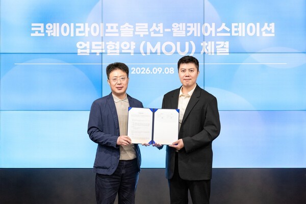
Coway Life Solution CEO Kim Myung-gon, left, and Wellcare Station CEO Kook Kyung-min pose for a photo at a memorandum of understanding signing ceremony at G-Tower in Guro, Seoul, on Sept. 8. (Photo: Coway)
Coway Life Solution CEO Kim Myung-gon, left, and Wellcare Station CEO Kook Kyung-min pose for a photo at a memorandum of understanding signing ceremony at G-Tower in Guro, Seoul, on Sept. 8. (Photo: Coway)
Coway Life Solution is partnering with integrated home care provider Wellcare Station to expand care services for customers with dementia and long-term care needs.
Coway Life Solution said Sept. 9 it signed a memorandum of understanding with Wellcare Station to support home care services for senior customers who need care and their families.
Wellcare Station is an integrated home care provider where doctors, nurses and care workers collaborate to provide home nursing and home care services. It also offers in-home care services including hospital accompaniment and support for using South Korea’s long-term care family leave program.
Under the agreement, Coway Life Solution customers with family members who require continuous care due to dementia or other conditions can receive support for long-term care services.
The service covers checking eligibility for the long-term care family leave program, connecting customers with care workers and coordinating schedules. For customers without a long-term care grade, it also handles related administrative procedures, including preparing documents needed to apply for a grade and filing applications with the National Health Insurance Service.
Wellcare Station will operate a dedicated service channel for Coway Life Solution customers. Customers using home care services will also receive priority assignment of care workers on their preferred dates.
Coway Life Solution is also expanding dementia care and caregiving support for senior customers. In partnership with digital healthcare company Silvia Health, it provides cognitive function assessments and personalized cognitive training. It also has partnerships with caregiving and long-term care providers Caring and Caredoc.
“We will help Coway Life Solution customers access long-term care-related services more conveniently,” Wellcare Station CEO Kook Kyung-min said.
AI glasses jointly developed by Samsung Electronics and Google. (Photo: Samsung Electronics)
AI glasses jointly developed by Samsung Electronics and Google. (Photo: Samsung Electronics)
Samsung Electronics has begun developing its first artificial intelligence glasses equipped with a display. The device is designed to show color visual information across the front of the lens.
Samsung Electronics asked Samsung Display last month to develop a microdisplay for AI glasses, according to industry sources on Sept. 9. It provided requirements covering the product form factor, information display area, color and price.
Samsung is expected to evaluate the performance and cost of panels that meet its requirements, including OLED-on-Silicon (OLEDoS) and LED-on-Silicon (LEDoS). Industry officials expect the product to launch in the second half of next year or the first half of 2028, with the timing depending on panel development and product validation.
Samsung has considered an ultra-small panel measuring 0.2 inch or less that can fit inside an eyeglass frame. An optical system would magnify the panel image and deliver it to the user’s eye. The device is intended primarily to display simple information such as text, notifications, icons and navigation arrows. Samsung has yet to decide whether to use a binocular design with displays for both eyes or a monocular design for one eye.
Rather than a high-resolution display capable of finely reproducing colors and contrast, Samsung is pursuing limited gradation of about 4 bits. Gradation refers to the number of brightness levels. Four bits per color channel provides 16 levels, compared with 256 levels for 8 bits. The approach is expected to prioritize easy recognition of text and symbols rather than rich colors for photos and video.
Industry officials consider white OLEDoS a practical option in terms of cost and production yield. OLEDoS is an ultra-small display that forms organic light-emitting diodes (OLEDs) on a silicon substrate. The white approach combines white OLEDs with color filters to produce colors. RGB OLEDoS does not require color filters but is more difficult to manufacture at high yields and carries higher production costs.
LEDoS combines microscopic light-emitting diodes (LEDs) with a silicon substrate. Its strength is high brightness, but color reproduction and mass-production yields remain challenges. It also requires technologies such as integrating red, green and blue (RGB) elements or converting light from blue LEDs into red and green.
Another technical challenge is securing a wide field of view (FOV), which determines the angular range over which users can see the virtual display. Because Samsung wants information displayed across the front of the lens, the viewing angle must also be wide. The product must achieve this while meeting color and cost requirements.
Samsung is planning the AI glasses as a smartphone companion accessory, keeping the smartphone as the primary device while allowing users to view necessary information through the glasses.
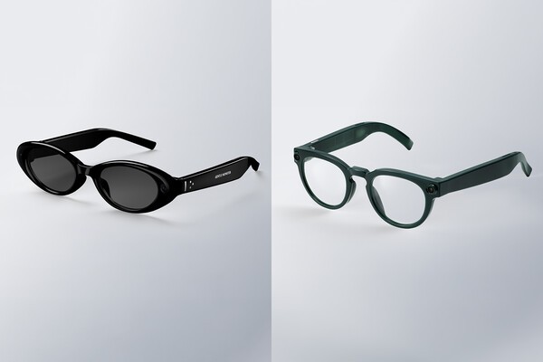
Samsung’s first AI glasses, scheduled for release this year, operate without a display and focus on camera and voice functions. They were jointly developed with Google, Gentle Monster and Warby Parker, combining Samsung’s hardware engineering, Google’s AI technology and designs from the two eyewear brands.
Meta commercialized color-display AI glasses in September last year. Meta Ray-Ban Display uses a monocular design with a screen only in the right lens. The display has a resolution of 600×600 pixels and a 20-degree FOV. Its full-color screen can display messages, photos, maps and translated subtitles, with the display positioned to the side of the user’s field of vision to avoid obstructing the forward view. Samsung, by contrast, plans to display text and symbols across the front of the lens using limited gradation.
“Samsung plans to evaluate OLEDoS, LEDoS and other panels that meet its requirements before commercializing the product,” an industry official said. “Samsung has not specified a particular panel technology, but RGB OLEDoS presents significant cost and production-yield challenges. Realistically, white OLEDoS is the more likely option.”
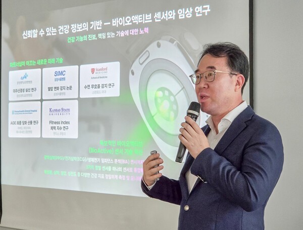
Choi Jong-min, executive vice president of the Digital Health Team at Samsung Electronics’ MX Business, introduces heart health management technologies for Galaxy Watch and the Samsung Health app. (Photo: Samsung Electronics)
Choi Jong-min, executive vice president of the Digital Health Team at Samsung Electronics’ MX Business, introduces heart health management technologies for Galaxy Watch and the Samsung Health app. (Photo: Samsung Electronics)
Samsung Electronics has expanded heart health management features based on its Galaxy Watch devices and Samsung Health app.
Samsung introduced features including blood pressure and electrocardiogram (ECG) measurement, a heart health score, vital signs monitoring and health data sharing among family members at a media briefing held Sept. 9 at the Taepyeong-ro Building near Seoul City Hall.
Samsung introduced an optical photoplethysmography (PPG) sensor with the Galaxy S5, Gear 2 and Gear Fit in 2014 and has since continued to expand its health management technologies. In 2020, its Samsung Health Monitor app for blood pressure and ECG measurement received medical device approval from South Korea’s Ministry of Food and Drug Safety.
In 2021, Samsung introduced the BioActive Sensor on the Galaxy Watch4, combining optical heart rate, ECG and bioelectrical impedance analysis (BIA) sensors. In 2023, its Irregular Heart Rhythm Notification feature, which alerts users to signs of possible atrial fibrillation, received clearance from the U.S. Food and Drug Administration (FDA) and South Korea’s Ministry of Food and Drug Safety.
The Galaxy Watch Ultra2 and Watch9 support a heart health score feature. It analyzes health data including sleep, activity levels, vascular stress and body composition to provide a score and health management guidance.
The devices also support a vital signs feature that tracks physical conditions during sleep. It measures five indicators — heart rate, heart rate variability, respiratory rate, skin temperature and blood oxygen saturation — and alerts users when changes differ from their usual baseline.
Samsung Health also includes health data sharing. With user consent, data including steps, exercise, sleep, weight, body composition, food intake, heart rate, stress, blood pressure, blood glucose, medication and vital signs can be selectively shared with family members or acquaintances.
Linking family profiles with Samsung accounts allows family members to view one another’s health records.
Samsung also disclosed real-world examples of the features in use. In Jordan last year, a user discovered atherosclerosis and underwent a procedure after receiving an irregular heart rhythm notification. In Brazil, a user who repeatedly received inconclusive ECG readings sought medical attention and addressed the risk of myocardial infarction, Samsung said.
“We are combining Galaxy Watch sensor technology with Samsung Health’s analytical capabilities to help users manage heart health risk factors,” said Choi Jong-min, executive vice president of the Digital Health Team at Samsung Electronics’ Mobile eXperience (MX) Business. “We will introduce smart healthcare services focused on prevention.”
A second-generation production line at the Display Innovation Process Center. (Photo: THE ELEC)
A second-generation production line at the Display Innovation Process Center. (Photo: THE ELEC)
The Display Innovation Process Center at Chungnam Techno Park is starting revenue-generating operations. The center aims to secure operating funds following completion of its infrastructure project by attracting demand for process development, prototype production support and materials evaluation.
According to Chungnam Techno Park on Sept. 8, the center is developing an operating model under which three to five companies would continuously use its fab. It plans to provide various processes according to each company’s development schedule while supporting individual process evaluations for other companies between equipment-use periods. The goal is to maintain a steady equipment utilization rate.
The center plans to cover operating expenses through equipment-use fees and follow-up research and development projects. Electricity alone costs about 1.3 billion to 1.5 billion won annually. Equipment must remain powered even when not in use to maintain its condition, while air conditioning, cooling and wastewater treatment also add costs.
Passing all fixed costs on through usage fees would impose a heavy burden on companies that require only small samples. The individual publicly funded projects currently underway are also too small to cover operating expenses. The center plans to pursue corporate development projects alongside large-scale follow-up projects.
The center opened in April last year and completed setup of individual processes around October. It began full-scale support for materials, components and equipment companies this year. The center is currently preparing the final report for its infrastructure project and coordinating schedules for internal performance reviews with relevant organizations.
CLAP, a tenant company, is using the center’s fab and office space to develop prototypes with the goal of supplying a South Korean automaker. It has also relocated its chemical synthesis laboratory to the center. CLAP is responsible for product development, while the center provides facilities and process support. Several other companies have also expressed interest in using the production line, and the center is discussing equipment and process support tailored to their development needs.
The center is addressing demand from both companies that need only individual processes and those seeking to relocate their development operations. Its model combines individual equipment-use fees with revenue from projects that provide long-term process development and prototype production support.
The center has also secured evaluation projects linked to Samsung Display. Samsung Display used laser equipment at the center to evaluate a crystallization process and confirmed favorable results. It has also advised suppliers of polyimide (PI) materials for flexible organic light-emitting diode (OLED) substrates to provide evaluation data generated at the center.
The center provides process equipment and analytical facilities to materials, components and equipment companies that have difficulty securing opportunities for customer evaluations. Companies can verify the process characteristics of products under development without building their own fabs. Equipment utilization has increased as a result. From last year through April this year, 85 companies used the facilities, excluding duplicates. Process equipment utilization rose to a cumulative 65.8% as of April this year from 59.7% last year, while utilization of testing and evaluation equipment increased to 73.3% from 64.0%.
The center is also carrying out eight projects, including government-funded programs, to prepare for emerging technologies. In a project to develop 2,500-pixels-per-inch (PPI) glass-based displays, researchers are evaluating the characteristics of technologies originally developed on wafers when applied to second-generation rectangular substrates.
Researchers aim to improve the cost and productivity of displays for extended reality (XR) applications through ultra-high-resolution glass-based processes. The center is also supporting a project to develop immersive spherical free-form displays by implementing foundational technologies on second-generation substrates.
The center also operates professional training programs. It trained 122 people through its Display Academy last year and aims to train 150 this year. Courses cover OLED process equipment, oxide processes and materials analysis. Current three- and five-day programs provide explanations of the entire process and opportunities to observe equipment inside the fab. To expand the scope of corporate support, the center is establishing process conditions required to produce complete panels. It has evaluated red, green and blue (RGB) illumination using its own test substrates and produced prototypes for exhibition.
Corporate support currently focuses on individual processes and multilayer structure evaluations. The center has yet to establish a track record of supporting companies through an integrated end-to-end process. Engineers are repeatedly conducting deposition and patterning while adjusting film quality, alignment and etching conditions.
The central government, local governments and the private sector have invested a total of 528.1 billion won since 2019 in the Display Innovation Process Platform project, including 377 billion won in central government funding. The project includes R&D for core OLED technologies and construction of the center’s infrastructure. The center is equipped with 65 units across 63 types of process, testing, evaluation and utility equipment.
“The center’s role is to evaluate products developed by materials, components and equipment companies so they can secure preliminary data to present to Samsung Display and LG Display,” said Jung Byung-hwa, head of the Display Innovation Process Center. “Our engineers can also enhance their technical capabilities by responding to requests from various companies and evaluating process results.”
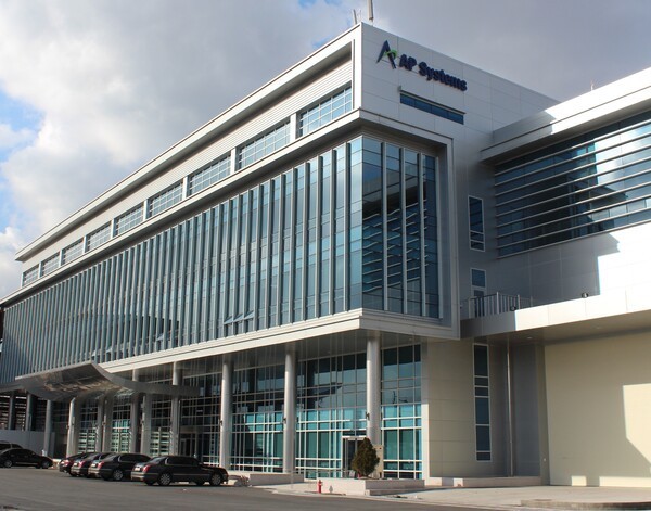
AP Systems has formed an open innovation fund to identify companies in deep technology and the materials, components and equipment sectors.
AP Systems said Sept. 8 that it formed the Gravity-AP Systems Open Innovation Investment Partnership No. 1 with venture capital firm Gravity Ventures.
The fund will combine AP Systems’ technology and commercialization capabilities with Gravity Ventures’ expertise in identifying and investing in deep-tech startups. Gravity Ventures will handle company sourcing, investment screening and execution, and post-investment management, while AP Systems will support technology reviews and business cooperation.
Investment targets will include deep-tech and materials, components and equipment companies that can be linked to AP Systems’ existing and new businesses. The two companies will also pursue business cooperation from the investment review stage, including proof-of-concept (PoC) testing, joint development and supply-chain integration.
Key areas under consideration include advanced laser and optical application technologies, advanced semiconductor packaging and back-end process solutions, artificial intelligence (AI)-based smart manufacturing and process intelligence, AI-based automated optical and visual inspection (AOI and AVI), physical AI and robotics-based factory automation, and technologies for advanced materials, defense and medical applications.
Portfolio companies will be given opportunities to use AP Systems’ manufacturing infrastructure and industry network for technology validation and field deployment, as well as cooperation in commercialization and mass production. AP Systems aims to secure technologies applicable to industrial sites at an early stage and expand links between its existing and new businesses.
Gravity Ventures has invested in early-stage companies in deep tech, semiconductor materials, components and equipment, and physical AI. In the first half of this year, it operated “Gravity Pulls,” a program to identify and foster startups in those fields.
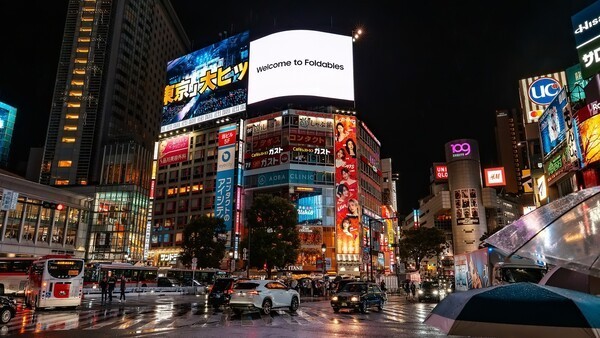
Samsung Electronics’ “Welcome to Foldables” outdoor advertisement featuring the Galaxy Z Fold8 series in Shibuya, Tokyo. (Photo: Samsung Electronics)
Samsung Electronics’ “Welcome to Foldables” outdoor advertisement featuring the Galaxy Z Fold8 series in Shibuya, Tokyo. (Photo: Samsung Electronics)
Samsung Electronics is running a “Welcome to Foldables” outdoor advertising campaign featuring its Galaxy Z Fold8 series in major cities around the world.
Samsung Electronics said Sept. 8 that it has been rolling out digital outdoor advertisements since Sept. 2 at six major landmarks, starting with KT Square in Gwanghwamun, Seoul, followed by K-POP LIVE at COEX, Shibuya Station in Tokyo, and Piccadilly Circus and Outernet in London.
The advertisements feature three messages: “Ultra Thin,” “The world’s lightest fold” and “Built to outlast.”
Samsung Electronics has developed its foldable products over eight generations since launching its first Fold model in 2019. The Galaxy Z Fold series has evolved with software optimized for the foldable form factor, artificial intelligence (AI) and connectivity across Galaxy devices.
The latest Galaxy Z Fold8 series set a record for Galaxy smartphone pre-orders in South Korea. The series is currently sold in 106 markets worldwide.
KAIST Professor Kim Sang Kyu (left) and Gyeongsang National University Professor Kim Yun Hee. (Photo: Toray Advanced Materials Korea)
KAIST Professor Kim Sang Kyu (left) and Gyeongsang National University Professor Kim Yun Hee. (Photo: Toray Advanced Materials Korea)
The Korea Toray Science Foundation has selected the winners of the 9th Korea Toray Science and Technology Award.
The foundation said Sept. 8 that it selected KAIST Professor Kim Sang Kyu in the basic research category for chemistry and materials and Gyeongsang National University Professor Kim Yun Hee in the applied research category. Each will receive 100 million won in prize money.
Kim Sang Kyu developed experimental techniques to observe changes in chemical reactivity depending on molecular structure. He was recognized for elucidating the structural dynamics of transition states and conical intersections that determine chemical reaction rates. He has also conducted research into electron-nuclear correlations by controlling electrons in anions.
Kim Yun Hee has conducted research on the synthesis of organic semiconductor materials. She secured core technology for high-efficiency deep-blue organic light-emitting diode (OLED) materials and was recognized for contributing to the localization of materials and the development of related technologies and human resources through industry collaboration.
The foundation also selected five early-career scientists for the Korea Toray Fellowship. Each researcher will receive a total of 150 million won in research funding over three years.
In the basic research category, DGIST Department of Chemistry and Physics Professor Song In Taek and Seoul National University Department of Chemistry Professor Hong Seung Youn were selected. In the applied research category, Sogang University Department of Chemical and Biomolecular Engineering Professor Kim Hyung Jun, POSTECH Department of Materials Science and Engineering Professor Chun Dong Won and Hanyang University Department of Chemical Engineering Professor Ham Dong Hyo were selected.
The foundation selected the recipients after soliciting nominations from April through June and evaluating candidates based on their academic achievements, originality and potential contributions to future advances in science and technology. The awards ceremony will be held in October.
The Korea Toray Science Foundation was established in 2018. Including this year's recipients, it has selected 18 winners of the Korea Toray Science and Technology Award and 40 fellowship researchers. The foundation also provides scholarships to 30 science and engineering students each year and has supported a cumulative 255 students through the second semester of 2026.
Coway’s Zero Food Waste Processor Microbial Type. (Photo: Coway)
Coway’s Zero Food Waste Processor Microbial Type. (Photo: Coway)
Coway is expanding its food waste processor lineup from grinding-type models to microbial systems.
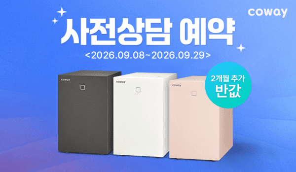
Coway said Sept. 8 that it will accept advance consultation reservations through Sept. 29 for its Zero Food Waste Processor Microbial Type, scheduled for launch later this month.
The new product uses microorganisms inside the unit to continuously break down and reduce food waste. Users can add waste whenever it is generated, while the remaining byproducts need to be removed once every one to three months.
The product is designed for immediate use after installation without a separate microorganism cultivation period. It uses a high-capacity activated carbon filter and patent-pending microorganisms extracted from traditional Korean fermented sauces. The system removes 99% of eight types of odors and harmful gases generated during food waste processing.
The unit is 24 centimeters wide and can process up to 0.7 kilograms of food waste per day. It is available in three colors: Porcelain White, Dark Gray and Mild Pink.
Customers can choose between in-home maintenance visits by Coway’s Cody service staff or self-maintenance. Rental customers will receive one additional supply of the microbial agent during the rental period.
Customers who make an advance consultation reservation and sign up for a new rental will receive an additional 50% discount on rental fees for two months.
The Zero Food Waste Processor Microbial Type is eligible for government subsidies for food waste reduction equipment. Customers purchasing the product outright may receive partial reimbursement of the purchase cost, depending on the criteria set by their local government.
Chinese display maker BOE is seeking to supply organic light-emitting diode (OLED) panels for Apple's iPad Air, following Samsung Display's lead into the product lineup.
According to industry sources on Aug. 11, BOE is developing OLED panels for the next-generation iPad Air, which is expected to be unveiled in the first half of next year. Development is taking place at the company's B12 production facility in Chongqing, China, where its sixth-generation OLED production line is located.
Apple has selected Samsung Display as the primary supplier of OLED panels for the iPad Air and is expected to begin mass production around the end of this year or early next year. BOE is aiming to secure a secondary supplier position alongside Samsung Display. The company has not yet reached the mass production qualification stage and is expected to submit samples for evaluation before undergoing Apple's qualification process. A final decision on commercial supply is expected around the end of this year. Initial shipments could be limited to models for the Chinese market or refurbished devices.
Industry sources expect BOE's mass production qualification to be determined in November or December. Apple typically grants production approval one to two months before mass production begins. If BOE fails to qualify, Samsung Display is expected to become the sole supplier for the initial production run.
BOE has previously supplied OLED panels for Apple's iPhone lineup. In the IT OLED segment, including iPads, however, South Korean manufacturers such as Samsung Display and LG Display have maintained the leading positions.
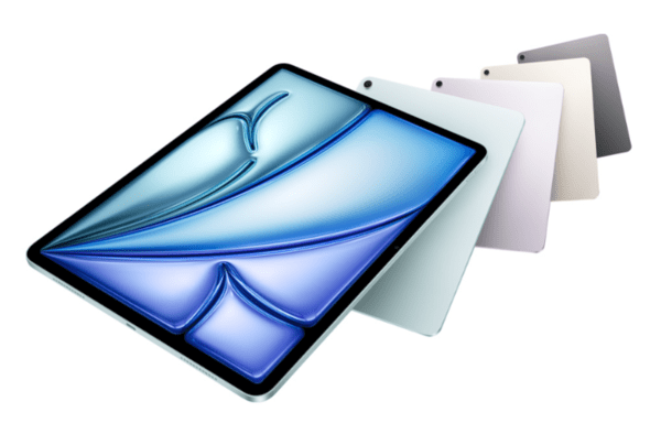
The new iPad Air is being developed in 11-inch and 13-inch versions. It is expected to adopt a hybrid OLED panel combining a glass substrate with thin-film encapsulation (TFE). The display will likely use a single-stack red-green-blue (RGB) emitting structure, while the thin-film transistor (TFT) backplane will be based on low-temperature polycrystalline silicon (LTPS). The panel is also expected to support a 60-hertz refresh rate.
Apple has differentiated the iPad Air from the iPad Pro by adopting a single-stack OLED architecture and LTPS technology, reducing panel costs while maintaining OLED display quality. As Apple expands OLED adoption from the iPad Pro to the iPad Air, the tablet OLED market is expected to continue growing.
According to market research firm Omdia, shipments of OLED panels for tablets are projected to increase 39% to 15 million units this year from 10.9 million units last year. By contrast, liquid crystal display (LCD) panel shipments are expected to remain largely flat, with OLED driving overall growth in the tablet display market.
"BOE is developing OLED panels with the goal of entering the iPad Air supply chain," an industry source said. "Whether it ultimately secures supply orders, and in what volume, will depend on Apple's evaluation and mass production qualification results."
Separately, BOE is also seeking to supply OLED panels for Apple's MacBook Pro from its B16 8.6-generation OLED production line in Chengdu. However, the company is reportedly still facing challenges in stabilizing manufacturing yields, making commercial shipments to Apple unlikely in the near term. Industry sources expect BOE to enter Apple's MacBook Pro OLED supply chain after 2028.
Samsung Electronics has opened a permanent exhibition highlighting the technological and design evolution of its Galaxy foldable smartphones over the past seven years.
The company said on Aug. 11 that it began operating the Foldable Heritage exhibition on Aug. 10 on the third floor of Samsung Gangnam. Permanent exhibition spaces have also opened on the first floors of Samsung Store Hongdae and Samsung Store Cheongdam.
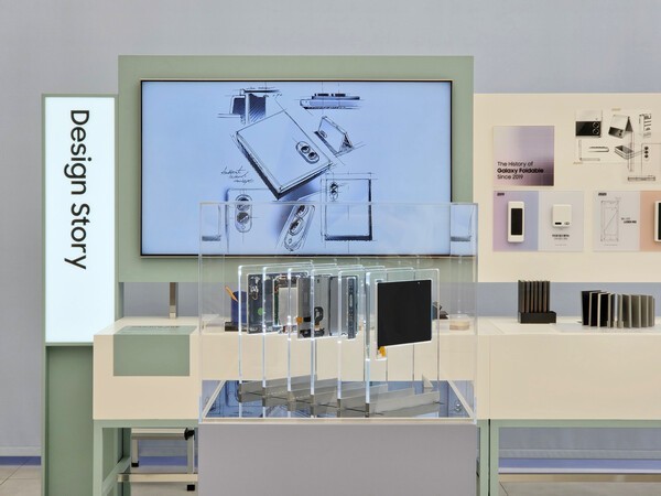
The exhibition is divided into three sections: Galaxy Fold & Flip Story, Design Story and Tech Story.
The Galaxy Fold & Flip Story section showcases the evolution of Samsung's foldable devices and technologies, beginning with the original inward-folding Galaxy Fold, introduced in 2019, through the Galaxy Z Trifold and the recently launched Galaxy Z Fold8. The exhibition also highlights the development of Galaxy AI and other software technologies.
The Design Story section reveals the development process behind the Galaxy Z Fold8 Ultra, Galaxy Z Fold8 and Galaxy Z Flip8, featuring early design sketches, mock-up testing, aspect ratio studies and the decision-making process behind the products' final designs. The Tech Story section focuses on advances in foldable display and hinge technologies, including Samsung's Flex Titanium technology used in the Galaxy Z Fold8 Ultra and Galaxy Z Fold8, presented through product displays and video demonstrations.
Visitors can also watch videos of durability tests conducted during product development, including folding, water-resistance and impact testing. In addition, Samsung is displaying disassembled Galaxy Z Fold8 Ultra and Galaxy Z Fold8 devices to showcase their internal components and structural design.
Park Jung-mi, Executive Vice President and Head of Samsung Electronics Korea, said the exhibition was designed to allow visitors to experience the company's accumulated foldable technologies and development process over the past seven years.
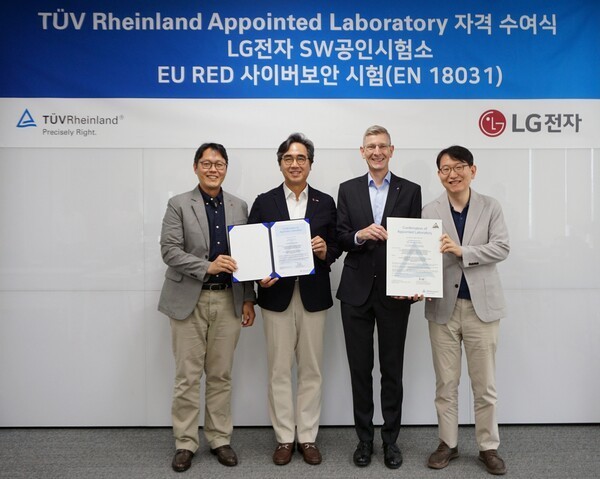
From left, Shim Woo-gon, head of LG Electronics' SW Engineering Research Center; Kim Dong-wook, head of LG Electronics' SW Center; Frank Juettner, chief executive officer of TÜV Rheinland Korea; and Lim Hyo-jun, head of LG Electronics' Next-Generation Computing Research Center, pose at a qualification award ceremony held at TÜV Rheinland Korea headquarters on Aug. 10. (Photo: LG Electronics)
From left, Shim Woo-gon, head of LG Electronics' SW Engineering Research Center; Kim Dong-wook, head of LG Electronics' SW Center; Frank Juettner, chief executive officer of TÜV Rheinland Korea; and Lim Hyo-jun, head of LG Electronics' Next-Generation Computing Research Center, pose at a qualification award ceremony held at TÜV Rheinland Korea headquarters on Aug. 10. (Photo: LG Electronics)
LG Electronics has secured an in-house testing qualification for cybersecurity requirements under European wireless device regulations, allowing it to proceed with certification based on its own test results without sending products to overseas testing organizations.
LG Electronics said on Aug. 11 that its Software Testing Center under the chief technology officer (CTO) organization has been designated by TÜV Rheinland as a testing laboratory for cybersecurity requirements under the European Union's Radio Equipment Directive (RED).
The RED requires wireless communication products sold in Europe to meet security and safety requirements. Cybersecurity provisions related to network protection, personal data protection and financial fraud prevention were strengthened in 2025.
With the new qualification, LG Electronics' Software Testing Center can conduct the relevant certification tests internally. TÜV Rheinland will review the company's submitted test results and data and can issue certification without conducting a separate test.
The process allows LG Electronics to reduce the time and cost required from product development through certification and launch because prototypes no longer need to be sent to overseas certification bodies. It also limits the amount of product information that must leave the company. For business-to-business (B2B) operations such as automotive components and HVAC systems, the company expects to shorten certification procedures for products customized to client requirements.
LG Electronics has continued to expand its software regulatory compliance capabilities. In 2019, it obtained international accredited testing laboratory status in the software field from the Korea Laboratory Accreditation Scheme (KOLAS) and subsequently broadened its testing scope to home appliances, automotive functional safety and cybersecurity.
The company is also seeking accredited testing laboratory status for the European Union's Cyber Resilience Act (CRA), which is scheduled to take effect in 2027. The CRA establishes cybersecurity requirements for products containing digital elements regardless of whether they support wireless communications.
LG Electronics is also strengthening its product security framework. Through LG Shield, the company manages product security from the development stage through post-launch operation. It provides patches for vulnerabilities discovered after release and is applying post-quantum cryptography technologies designed to address future threats from quantum computers.
LG SIGNATURE OLED W displayed in a ground-floor storefront window at Harrods in London. (Photo: LG Electronics)
LG SIGNATURE OLED W displayed in a ground-floor storefront window at Harrods in London. (Photo: LG Electronics)
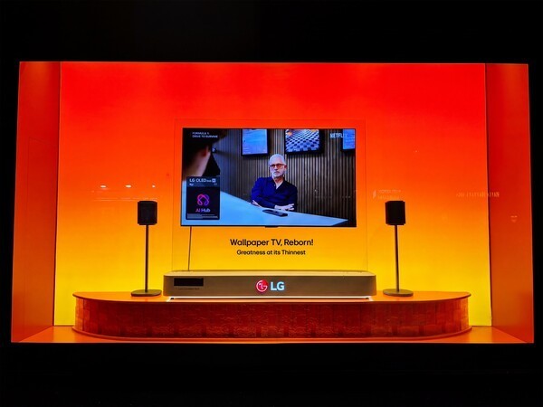
LG Electronics said on Aug. 10 that it is holding a special exhibition for its next-generation wireless wallpaper TV, the LG SIGNATURE OLED W, at the Brompton Road display windows on the ground floor of Harrods through Aug. 26.
The exhibition is being held in the department store's Brompton Road storefront windows, which attract approximately 1.1 million visitors per month. LG Electronics designed the exhibition route so that visitors who view the product in the display windows can continue to experience it inside the company's retail space within the department store.
The LG SIGNATURE OLED W achieves a thickness in the 0.9-centimeter range by minimizing the size of key components, including the display panel, power board and speakers. Video signals are transmitted wirelessly through LG's Zero Connect Box, which connects to peripheral devices. The company said the Zero Connect Box is 35% smaller than those used with its previous wireless TV models.
The television can wirelessly transmit content at up to a 165 Hz refresh rate in 4K resolution. It is powered by LG Electronics' third-generation Alpha 11 AI processor for image and sound processing. According to the company, the processor delivers 5.6 times greater neural processing unit (NPU) performance and a 70% improvement in graphics processing performance compared with the previous generation.
The LG SIGNATURE OLED W has received Intertek's Reflection Free Premium certification and TÜV Rheinland's True Wireless Low Latency Vision certification.
Coway's 8-pyeong wall-mounted air conditioner. (Photo: Coway)
Coway's 8-pyeong wall-mounted air conditioner. (Photo: Coway)
Coway said on Aug. 10 that it will offer rental fee discounts for new customers of selected products, including wall-mounted air conditioners, Zero Food Waste Disposers and Therasol U, through Aug. 26.
New customers renting Coway's wall-mounted air conditioner can receive a 50% discount on rental fees for up to 18 months. The product features four-way airflow control, power cooling, dehumidification, fan and sleep modes, as well as automatic drying and self-cleaning functions.
Customers who rent the 2-liter or 3-liter versions of the Zero Food Waste Disposer with grinder technology can receive a 50% rental fee discount for up to four months. The product includes a 150-degree heating system, four-blade grinding mechanism, activated carbon filter and UV-C sterilization function. Coway also provides one complimentary replacement of the drying container during the rental period.
Therasol U, a home-use medical device for urinary incontinence treatment, is available with a 50% rental fee discount for up to 12 months. The product has received approval from South Korea's Ministry of Food and Drug Safety and uses low-frequency electrical stimulation to induce contraction and relaxation of pelvic floor muscles and surrounding muscle groups.
Chinese display maker Visionox is preparing a follow-on investment for its 8.6-generation OLED production line, with industry attention focused on whether South Korean equipment suppliers such as YAS can secure orders after missing out on the first phase.
According to industry sources on Aug. 6, Visionox is planning a second-phase investment for its V5 fab under construction in Hefei, Anhui Province. While the exact timing has not been finalized, the project is widely expected to begin in the first quarter of 2027.
The V5 facility is designed for a total production capacity of 32,000 glass substrates per month. The first phase covers 8,000 substrates per month, while the second phase will add the remaining 24,000 substrates per month—three times the size of the initial investment.
The first phase included equipment supplied by South Korean companies such as AP Systems, SynusTech and ICD. Applied Materials (AMAT) won the order for the deposition equipment, widely considered the most critical tool in the production line. The company began delivering equipment in May and is currently conducting installation, commissioning and process validation for Visionox's ViP technology, a fine-metal-mask (FMM)-less OLED manufacturing process. Yield rates on the line are reportedly in the 30–40% range.
Although both AMAT and YAS deposit organic materials onto substrates by heating solid organic emissive materials in a vacuum environment, their approaches differ significantly.
AMAT uses a vertical deposition architecture in which 8.6-generation glass substrates are positioned upright during processing. The system integrates deposition, substrate transfer and encapsulation processes within a connected vacuum environment. Maintaining uniform film thickness across large vertically transported substrates is a key technical challenge.
YAS, by contrast, employs a horizontal architecture in which substrates remain flat while organic materials are deposited from evaporation sources located beneath them. The system maintains a constant distance between the evaporation source and substrate to ensure uniform film formation across the entire panel. As a result, chamber structures, transfer systems and overall equipment configurations differ substantially from those used by AMAT.
AMAT benefits from operational data and process conditions accumulated from the first-phase V5 line. If Visionox selects the same equipment for the expansion, previously developed deposition recipes and process parameters can be reused. Adopting YAS equipment, however, would require fresh validation of both equipment performance and manufacturing processes because of the different substrate-handling architecture.
Commenting on the possibility of YAS participating in the second phase, a Visionox official said, "We are currently validating the AMAT equipment, but yields remain low and pricing is high. If we adopt YAS equipment, we would need to conduct new verification work, so there are many factors to consider."
Visionox had also previously considered applying the conventional FMM process to portions of the V5 line. In May last year, the company discussed introducing FMM deposition equipment from Japan's Canon Tokki and South Korea's Sunic System. However, it ultimately chose the ViP approach.
According to Visionox, the likelihood of reverting to FMM technology in the second phase remains low.
Asked whether poor yields on the initial ViP line could lead the company to reconsider FMM technology, a Visionox official said, "Even if yields do not meet expectations, there is almost no possibility of returning to the FMM method. If we were to go back to FMM, it would raise questions about the rationale behind the investment, and we do not know whether the Hefei government would approve such a move."
Visionox is expected to determine the supplier for the second-phase deposition equipment based on the results of equipment installation, commissioning and ViP process validation on the first production line.
For the first-phase investment, Visionox selected lithography equipment from Canon, excimer laser annealing (ELA) and laser lift-off (LLO) systems from AP Systems, plasma-enhanced chemical vapor deposition (PECVD) and sputtering equipment from Applied Materials, and certain sputtering tools from ULVAC. Dry etching equipment was supplied by Tokyo Electron and ICD, while logistics and material-handling systems for array and deposition processes were provided by SynusTech.

 Login