COXEM, a scanning electron microscope (SEM) specialist, is transforming itself into a maker of nondestructive inspection equipment for advanced semiconductor packaging. The company has begun supplying modules for high-bandwidth memory (HBM) analysis and plans to introduce automated inspection equipment for panel-level packaging (PLP) and glass substrates.
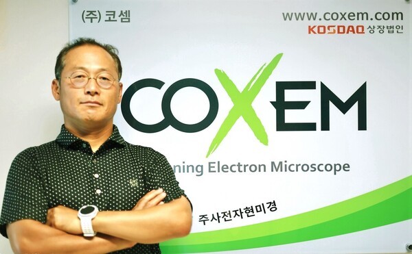
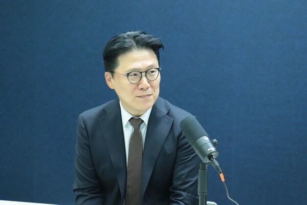
"The ion beam polisher, which precisely polishes semiconductor cross sections, was developed into equipment in collaboration with a domestic equipment company," COXEM CEO Lee Jun-hee said in a recent interview at the company's headquarters in Daejeon. "It has already been supplied to major semiconductor manufacturers and is undergoing mass-production evaluations."
COXEM, founded in 2007, is a South Korean developer and manufacturer of SEMs. The company started by licensing technology from the Korea Research Institute of Standards and Science (KRISS). It localized compact tabletop SEMs in the early 2010s and ranked fifth globally in sales in 2022, establishing its competitiveness in the market.
Lee, who holds a doctorate in electrical and electronic engineering from the Korea Advanced Institute of Science and Technology (KAIST), joined COXEM as head of its research center in 2010 and led research and development (R&D) of the technology. Lee was recognized for his technology development capabilities and business planning skills in 2012.
Ion Beam Polisher Module for HBM, MLCC Targets Qualification Early Next Year
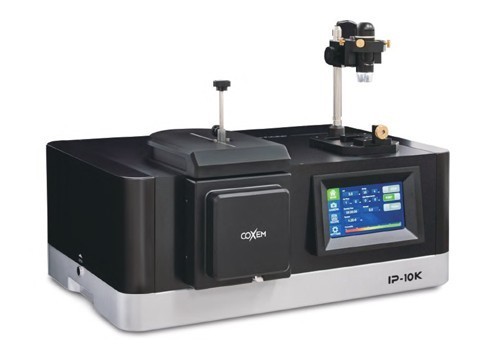
COXEM's IP-10K ion beam polisher. (Photo: COXEM)
An ion beam polisher is preprocessing equipment used to etch and polish a sample before it is examined with an electron microscope. It is based on ion miller commercialization technology that COXEM completed in 2019. COXEM's ion gun module, which emits an argon (Ar) ion beam, is installed inside the equipment. A separate SEM is also installed to observe and analyze the sample after preprocessing. AP Systems handles assembly and sales of the complete equipment.
Semiconductor analysis laboratories have traditionally polished sample cross sections manually, mainly using blades or sandpaper. The ion beam polisher automates the process. It uses a nanometer-scale particle beam to create flat cross sections without errors. It also minimizes sample damage and contamination compared with chemical mechanical polishing (CMP), preserving the sample's fine structures.
The system is similar to focused ion beam-scanning electron microscope (FIB-SEM) systems from global competitors such as Thermo Fisher Scientific and ZEISS, but differs in processing area and speed. FIB-SEM can precisely process extremely small areas of several micrometers or less and is suited to detailed analysis of nanoscale defects.
The ion beam polisher can rapidly remove material across areas as wide as several millimeters at a rate of 1,000 micrometers per hour. It can be used to inspect structures and defects including through-silicon vias (TSVs) and microbumps in HBM, as well as internal layers of multilayer ceramic capacitors (MLCCs). It is also less expensive. COXEM's CP-SEM lineup combining an ion miller and SEM costs about one-tenth as much as competing FIB-SEM systems.
"We initially guaranteed 100 hours of durability for the ion gun module, but have increased that to several thousand hours to meet the requirements of actual semiconductor mass-production lines," Lee said. "We expect to pass customer qualification tests around the end of this year or early next year and move into mass-production supply."
Nondestructive Inspection Equipment for Large Substrates Under Development
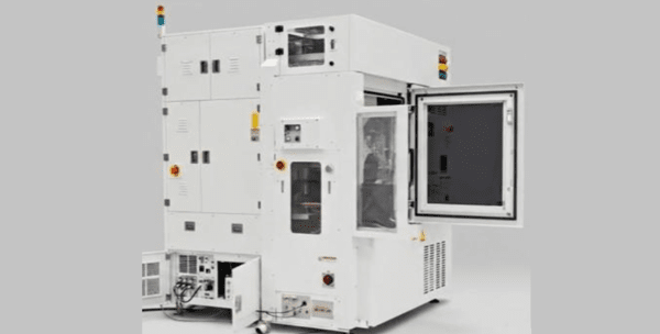
COXEM's Eirtron automated inspection equipment under development. (Photo: COXEM)
COXEM is also preparing semiconductor inspection equipment under its Eirtron brand. The equipment is designed for nondestructive observation of large-area samples, including wafers, large panels and glass substrates, during manufacturing. It is based on atmospheric-pressure scanning electron microscope (A-SEM) technology developed by COXEM.
Conventional inspection of large substrates requires cutting cross sections and moving them to an analysis laboratory. This is because conventional SEMs used for inspection rely on sealed high-vacuum chambers, limiting sample size. SEMs inspect samples by analyzing signals reflected from an irradiated electron beam. If the beam collides with air particles and scatters, the signal weakens and the detected image becomes blurred. High-vacuum chambers are used to prevent this.
A-SEM addresses this issue while maintaining high-resolution imaging with 30-nanometer resolution. This is achieved by completely separating the electron column, including the electron gun that emits the beam, from the external environment using a graphene membrane.
Graphene has high electron transmittance, allowing the beam to pass while blocking outside air. A multi-window structure allows it to withstand pressure of one atmosphere. The graphene membrane and signal detector are positioned as close as possible to the sample, while helium gas is injected to minimize electron-beam scattering and signal loss. These are all proprietary technologies patented by COXEM.
A-SEM can observe samples in ambient air at atmospheric pressure, eliminating size restrictions. It also removes the need for complex preprocessing steps such as evacuating a vacuum chamber or cutting samples, helping reduce process time.
"A-SEM technology enables real-time observation and analysis on production lines without damaging samples, making it an innovation that could shift the paradigm of semiconductor inspection processes," Lee said. "By commercializing automated A-SEM equipment, we aim to take the lead in the semiconductor equipment market currently dominated by overseas companies such as Applied Materials and Hitachi."
A test model of COXEM's automated equipment is currently undergoing validation by a major South Korean substrate company. The company plans to expand its target customer base to outsourced semiconductor assembly and test (OSAT) companies.
Coway employees and Gyeongil Elementary School students plant vegetation in the third Coway Ecological Forest. (Photo: Coway)
Coway employees and Gyeongil Elementary School students plant vegetation in the third Coway Ecological Forest. (Photo: Coway)
Coway has created an ecological forest featuring endangered and rare plants at Gyeongil Elementary School in Seongdong District, Seoul. The site will serve as an ecological learning space where students can observe plants and other living organisms.
Coway said on Sept. 16 that it created the third Coway Ecological Forest, covering about 365 square meters, on the school's grounds.
Coway planted 1,195 plants from 25 species, including endangered and nationally protected species such as Pseudolysimachion pusanensis, Hosta yingeri and Aster koraiensis. Coway employee volunteers and Gyeongil Elementary School students participated in the planting.
Environmental social enterprise Tree Planet and the Landscape Architecture Design Lab at the University of Seoul were responsible for the forest's design and construction. The ecological forest incorporates results from research collaboration between the two organizations.
Environmental education for students was also conducted after the forest was completed. Students observed the forest and completed ecological forest checklists. Coway selected 13 students as ecological forest gardeners and provided them with garden maintenance kits.
Coway operates an ecological forest program that plants endangered and rare species in South Korea designated by the International Union for Conservation of Nature (IUCN) and the Korea Forest Service, as well as plants endemic to the Korean Peninsula. The company created its first ecological forest in an outdoor space at its headquarters in 2024 and its second at Banghwa Elementary School in Seoul last year.
Coway also operates environmental social contribution programs including Clean School Classroom Forest, which provides air-purifying plants to elementary schools; river plogging to collect waste along waterways; and the throwing of effective microorganism (EM) mud balls to improve water quality.
Hanwha Aerospace has successfully completed a mock combat flight in South Korea of the Mojave STOL, a short-takeoff-and-landing unmanned aircraft system (UAS) it is jointly developing with General Atomics Aeronautical Systems, Inc. (GA-ASI).
Hanwha Aerospace said the Mojave took off from the Republic of Korea Army's 513th Aviation Battalion airfield during the 2026 Defense Drone Technology Exhibition in Pocheon, Gyeonggi Province, on Sept. 16 and landed on a tank maneuver road. The aircraft then took off again from the site and returned to the airfield.
The Mojave is equipped with a 450-horsepower turboprop engine and high-lift devices, allowing it to take off and land within distances of 100 to 300 meters. During the demonstration, it took off in less than 200 meters and landed within a distance in the 100-meter range.
The Mojave can carry up to 1 metric ton of mission equipment. Depending on its equipment configuration, it can be used for ground attack, intelligence, surveillance and reconnaissance, logistics transport and communications relay missions.
Hanwha Aerospace plans to establish R&D and production infrastructure for the Mojave in South Korea. The company aims to raise the share of domestic production to more than 70% once the aircraft enters mass production.
YMC, a maker of components and materials for semiconductor and display equipment, plans to distribute at least 15 billion won in dividends to shareholders over three years starting this year.
YMC disclosed the shareholder value enhancement plan on Sept. 16. The company updated a plan announced in April, setting numerical targets for shareholder returns.
YMC will use 30% of net income as a source for dividends. It also set a minimum dividend level. The company plans to pay at least 5 billion won annually from this year through 2028, for a cumulative total of at least 15 billion won over the three years.
The company will also continue to cancel treasury shares. YMC canceled 500,000 treasury shares in March and plans to cancel at least another 630,569 shares by year-end, equivalent to about 50% of the 1,261,138 shares it currently holds. If completed as planned, the total number of shares outstanding will decline by at least 3.32%. Including shares canceled in February 2023, cumulative cancellations are expected to exceed 1.63 million shares.
YMC has also established a system to monitor implementation of its shareholder value enhancement plan. The company will carry out the plan under the management and supervision of its board and conduct a self-assessment at least once a year, disclosing its implementation status. It also plans to expand investor communications through domestic and overseas investor relations events and press releases.
"The shareholder value enhancement plan demonstrates our strong confidence in improving the company's future performance and our commitment to shareholder returns," YMC said. The company posted consolidated revenue of 100.5 billion won and operating profit of 3.89 billion won in the first half of 2026, up 19.2% and 55.3%, respectively, from a year earlier. A new semiconductor plant in Dangjin, South Chungcheong Province, completed last year, began full-scale mass production this year, driving revenue growth and improved profitability.
YMC manufactures and supplies diffusers and susceptors for chemical vapor deposition (CVD) equipment as well as vacuum equipment components. Diffusers uniformly distribute gas inside process equipment chambers to help form even thin films on treated surfaces or facilitate etching. Susceptors support wafers or substrates to maintain uniform temperatures during thin-film deposition.
Je-hwang Ryu, CEO of CATBeamTech. (Photo: THE ELEC)
Je-hwang Ryu, CEO of CATBeamTech. (Photo: THE ELEC)
CATBeamTech has expanded its business beyond medical X-ray solutions into the semiconductor industry. Its core technology leverages Carbon Nanotube (CNT)-based X-rays to identify internal defects in High Bandwidth Memory (HBM).
CATBeamTech is currently conducting Proof of Concept (PoC) evaluations for its CNT X-ray equipment with domestic and international memory manufacturers. Upon receiving HBM sample wafers from memory makers, CATBeamTech images cross-sections to inspect for defects at specific locations. During performance verification, potential clients provide a mixed batch of normal and defective samples, and the equipment's performance is evaluated by comparing its classification results against the client's answer key.
HBM features a vertically stacked structure of DRAM chips in 4, 8, 12, or 16 layers. CATBeamTech identifies defects such as micro-bump failures connecting individual DRAM dies, die lifting, and warping.
As the number of stacked layers increases, early inspection becomes critical. Discovering a defect after completing the stacking process results in financial losses that compound across all preceding manufacturing steps. By identifying anomalies mid-process, CATBeamTech helps minimize these losses.
The observed defects are quantified: if the defect count exceeds normal thresholds, the system flags an anomaly for process management. "In the industry, there are rumors that certain memory makers' HBM yield is below 50%," said Je-hwang Ryu, CEO of CATBeamTech. "By tracking defect counts inside HBMs, we can help manage overall yield."
X-ray inspection is a non-destructive semiconductor testing method used to check for internal HBM defects. Through sampling inspection, process errors can be detected and addressed early. The system scans key points on a wafer to evaluate overall alignment and can trigger a secondary, high-precision inspection for suspicious areas. Companies like SEC and Zeiss also produce similar equipment.
CATBeamTech's primary advantage lies in its ability to build fully customized equipment. Parameters such as inspection speed and detectable defect size can be adjusted to client specifications because the company directly manufactures its own equipment, components, and CNT sources.
The equipment can detect defects ranging from 10 to 100 nanometers. According to CEO Ryu, competitors typically observe defects at the 500-nanometer level, giving CATBeamTech a precision advantage of 5 to 50 times. However, smaller defect detection involves a trade-off, such as longer inspection times. For commercialized products, CATBeamTech is developing technology optimized for 100-nanometer-level defect detection, balancing speed and resolution.
X-ray inspection works by transmitting electron-generated X-rays through the target object to observe its internal structure. CATBeamTech utilizes carbon nanotubes (CNTs) as its electron emitters. Traditional X-ray devices emit electrons by heating a filament, whereas CNTs emit electrons via an electric field without requiring thermal heating. Compared to filament sources, CNTs offer faster inspection speeds and are easier to miniaturize. They also enable precise output control, varying X-ray power based on the thickness and density of the target material.
With its CNT-based X-ray technology, CATBeamTech was selected by the Ministry of Small and Medium-sized Enterprises and Startups (MSS) as a promising semiconductor startup under the 'Deep-Tech Startup 1000+' project. Selected companies receive funding from the MSS for commercialization and R&D.
Q&A
Q: What is the Deep-Tech Startup Project?
A: It refers to sectors that the Ministry of Small and Medium-sized Enterprises and Startups (MSS) considers deep-tech, which includes semiconductors, defense, and healthcare. We were selected as a deep-tech company in the semiconductor sector, where they provide us with support. It allows us to further refine and systemize various technologies.
Q: Does the government give you money?
A: They give us funding, and they also serve as a bridge. They provide great guidance in terms of networking and connecting us with client companies.
Q: How much money do they give?
A: Around 1 billion KRW. We originally started with medical and component technology, so the industrial side was somewhat unfamiliar and was an area we didn’t know well. The project provided a great opportunity for us to enter this market rapidly.
Q: Were you selected because you already possess deep-tech technology? Or were you selected as one of the candidates to create deep-tech technology?
A: They look at both. Core technological capability is essential, and a company must possess materials or component technology. Furthermore, the derivative directions and applications must fall under deep-tech criteria to be selected.
Q: Could you please provide a brief introduction to your company and its proprietary technology?
A: Our company is a materials, components, and equipment company. For materials, we directly possess Carbon Nanotube (CNT) technology and synthesize CNTs in-house. Using CNTs, applications can extend to displays, X-rays, or even powder forms for other materials companies. However, our initial primary direction was chosen as X-rays.
We also manufacture X-ray components using electrons emitted from the tips of CNTs. Instead of importing X-ray sources, we possess various proprietary platforms. Because of this, just as bathroom, restaurant, and kitchen lightings are all different depending on their application, we can adapt our X-ray sources to fit specific needs—such as what semiconductor feature to look at, how high throughput needs to be, or how small or large of an object we need to observe.
Q: You previously appeared on our interview channel to introduce your CNT source X-ray technology and overall company background—viewers can refer to the link we’ll provide. You’ve used self-manufactured CNT X-ray sources to inspect internal structures and improve yields in sectors like batteries. I hear your recent focus is on HBM?
A: As the AI market grew dramatically, the world became covered in talks about artificial intelligence. With that, the need to look inside the HBMs used within core GPUs has grown significantly. The reason is that low yields are a widely known issue in this market, which also makes memory prices extremely expensive. Memory prices have risen considerably, but looking ahead, chips will be stacked up to 16 layers. If a problem occurs, the whole thing has to be thrown away.
If you build the 1st floor and inspect it, then build the 2nd floor and inspect it, and keep building if there are no issues, it works fine. But if there’s a problem on the 2nd floor and you keep building the 3rd, 4th, and 5th floors, that entire unit has to be discarded. That is why early inspection is currently so necessary.
Q: You compared it to an apartment, where each floor has structural components and plumbing connections. HBM is similar: if micro-bumps are poorly formed, cracked, or voided, electricity won't flow properly and causes failures. Your company's solution can observe this non-destructively, correct?
A: That is correct. Proper stacking means the micro-bumps are in their proper positions. If you look at a cross-section of the bumps using CT, you can count them. If they are misaligned, you won't be able to count the bumps normally in that cross-sectional view. Therefore, if this inspection goes well and allows normal counting across 2, 3, 4, up to 8 layers, the unit is confirmed as good. In short, processing the numerical values measured from images into statistical data—that is the direction our company is taking.
Q: Why do you process it statistically? Isn't it enough to just see if there is a defect?
A: Yes, seeing if there's a problem is the field called inspection. But in our field, metrology, numbers are key. Those numbers are ultimately converted into data linked directly to yield management. Usually, a separate team handles related tasks and manages yield by compiling statistics during device manufacturing.
Q: So inspection is "looking at it," and metrology is "counting it"?
A: Yes, exactly. Because it expresses exactly where and how a problem occurred as a number, it allows for proactive prevention. That difference is why we aim for metrology.
Q: You are a company that uses visual inspection to perform counting technology. One thing I wondered about is: isn't using X-rays to look inside HBM already a widely used technology? Companies like SEC and Zeiss are already in this market. Since everyone uses X-rays, I wondered what your differentiation is. Is it higher resolution, or are there other differences?
A: Obtaining X-ray images, building 3D volume data (CT data), and providing those results are the same. Our strength lies in directly possessing the X-ray source technology itself. It can be compared to a screwdriver: you need to use the exact right tool for the situation to identify problems quickly. This means our key advantage is providing solutions that perfectly match customer customization needs.
Recently, we have also been leveraging Artificial Intelligence (AI) technology to meet customer criteria—shooting images faster, lowering costs, improving visibility, and enhancing our overall customization capabilities. Companies like Zeiss mostly focus on general-purpose equipment. However, our advantage of being based in South Korea allows us to collaborate closely with clients here.
Q: You mentioned that holding the CNT source technology allows you to build equipment in whatever form the customer wants. What specific customer requirements might exist?
A: Even when looking inside HBM, requirements differ. In some cases, they only need to look at micro-bumps, while in others, they need to inspect die lifting or warping. Depending on the case, they might need to use a single X-ray source, five sources, or in extreme cases, around 50 sources. Accurately understanding customer needs and designing matching system structures to deliver solutions is our major point of differentiation from existing companies.
Q: How about speed and maintenance? Regarding lifespan, isn't CNT shorter compared to filaments?
A: Technology has advanced significantly, so lifespans are now at a similar level. Technically, filaments use a heating method, whereas carbon nanotubes can be viewed as digital X-ray sources. Filaments are analog technology, while CNTs are digital. Filaments are bulb technology, whereas CNTs are LED technology. A bulb setup uses only a single source because turning it on and off like digital equipment is difficult, so it stays continuously lit. In contrast, CNT technology can be turned on and off very easily.
Therefore, if multiple sources are required depending on the inspection target, they can be deployed as an array. If a certain area is thick or dense, we can use a stronger X-ray; if density is low, we can use a lower-output X-ray. Offering customized configurations is a massive advantage of CNT.
Q: For example, when getting a CT scan at a hospital, the machine rotates and takes time. Are you saying that instead of rotating the source, you can arrange sources in a circular array to capture images at once?
A: Exactly. X-ray sources used in hospital CT scanners are filaments, meaning there is only one X-ray source inside. Because it generates heat, it requires a cooling system. Then, large power modules called generators are needed.
It also requires high-grade bearings, and when all the mechanical components for maintaining stability are added up, it weighs several tons. When that technology transitions to digital, industrial applications gain the exact same benefits. Our company's starting point was originally to change the paradigm in the medical field, and we are now able to realize those same advantages in industrial fields.
Q: Is it true that your equipment can identify defects down to the 10-nanometer level?
A: We are a company holding technology solutions aimed at reaching the 10-nanometer domain. Competitors' typical specification is around 500nm, or 0.5 micrometers. We possess the core X-ray technology and focal point control technology mentioned earlier. Optical tech is required, and by harmonizing layout, magnification, and vibration control, we can observe down to 10 nanometers.
Q: Are you able to see down to 10 nanometers right now?
A: Yes, although 10 nanometers isn't visible with crystal-clear precision; it ranges between roughly 10 and 100 nanometers. Since other companies are usually around 0.5 microns, we can see much better. There is a market for high-end equipment that maximizes resolution, but equipment used in mass production lines has size limitations. Under those production constraints, 10 nanometers obviously cannot be seen.
Q: How long does it take to inspect a single HBM?
A: It depends on whether it is a 4-layer or 8-layer stack, but inspecting a single point usually takes about 10 to 60 minutes.
Q: What does "a single point" mean?
A: An HBM cross-sectional sample is about 10mm × 10mm in size, and we are looking at one specific point on that sample.
Q: Then clients cannot use this for 100% total inspection; they would use it for sample testing?
A: Correct. If it's a 300mm wafer, it has four quadrants. They can inspect them one by one or two by two to obtain information that represents the overall alignment state.
Q: So it would mainly be used during the development process?
A: Right. Some teams look at it during development, and some look at it at the final stage. I believe it must be used during development to catch yields effectively.
Q: Do you mean they take a rough look first, and if there seems to be a problem, they bring it over to take a precise image of that exact spot?
A: Exactly. The 1st step is a screening inspection, and the 2nd step is a precision inspection. In screening, they might use a fast CT scan or look only with basic X-rays.
Q: If a suspicious area appears under X-ray, do you perform statistical processing on that region?
A: We inspect only the suspicious area. We inspect the representative point, check a certain surrounding area, and then move on to the next process.
Q: Is there high market demand for this?
A: As known in the industry, current (HBM) yields are quite poor. Some companies are rumored to be below 50%. It's not great from a resource efficiency standpoint.
Q: Speaking as a non-expert, wouldn't doing 100% total inspection be more effective for boosting yield? Is total inspection not possible with X-rays?
A: It is possible. However, due to the current AI boom, even if chips are discarded, semiconductor makers' customers have enormous product demand and keep asking for continuous supply. That's why the current ecosystem was formed. But looking ahead at the next 10 years, normal manufacturing processes must include yield management. That way, our great domestic semiconductor makers can maintain their gap over China and latecomers while preparing for the future. We want to contribute with our core analysis and yield management technology.
Q: So you're saying they currently don't do total inspection. Is it because they can't, or because they choose not to?
A: Both. Defects aren't easily visible, and inspecting takes too much time.
Q: But your company's solution isn't a total inspection method either, is it?
A: Right now, we are at the PoC stage—demonstrating the concept and establishing the inspection logic.
Q: What point are prospective clients most interested in? Are they drawn to seeing finer details than others, or is it your proprietary source tech and faster inspection speed?
A: Clients have teams closer to R&D labs and teams closer to production factories. Naturally, R&D teams value precision even if speed is slower, while factory teams say, "It can be less precise, just make it fast." Both needs exist.
Speeding up the inspection makes images slightly less clear or blurry, while spending more time yields clearer images. It's a trade-off.
Q: Who are you currently talking with?
A: We are speaking with all major semiconductor clients, including Korean and US companies.
Q: They must be memory makers. When did discussions regarding HBM begin?
A: We started last year.
Q: How much does a single unit cost?
A: It depends on inspection speed and logistics integration, but prices generally range between 500 million and 3 billion KRW. If it needs to shoot fast while maintaining crisp clarity, it's 3 billion KRW; if it shoots relatively slowly with lower resolution, it's 500 million KRW.
Q: Are PoCs currently underway?
A: Yes.
Q: What does running a PoC entail? Are you receiving wafers and chips to inspect them, or is equipment installed on-site somewhere?
A: Customer requests are like: "We'll give you samples, show us what comes out." They ask for visualization data first.
Q: Do they tell you which specific points to capture?
A: They ask things like: "What can you see?", "Can you count the numbers?", etc.
Q: Can results be improved using AI as well?
A: We need to guide it toward enhancing both inspection precision and speed.
Q: So you receive samples, inspect them, send back the results, and continue that cycle?
A: Yes, we are continuously exchanging data. Inspecting HBM extracted from commercially available GPUs can be freely promoted. What we showed today is a sample from a disassembled Nvidia board we purchased, since client samples cannot be disclosed. Clients ask us questions while already knowing the correct answers.
Q: Meaning if it's a defective sample, the defect should show up?
A: They mix normal samples and defective samples together when handing them to us.
Q: It sounds like solving a puzzle. They evaluate whether you can see it or not?
A: Yes, so they already know the answer.
Q: Do they tell you how many points you got right?
A: Yes, they share the evaluation results with us.
Q: Are you getting 100 points right now?
A: Sometimes we get 50 points, and sometimes we get around 95 points.
Q: Why do the scores vary? Is it because points were captured incorrectly?
A: Sometimes they specify the points, and sometimes they don't. When inspecting at the 10-nanometer scale, there are countless points, so we scan an area of about 20 micrometers within a 100-micrometer field at a resolution capable of resolving 10-nanometer features.
If there's a void, we quickly catch that empty space, or if alignment is bad, we look for areas where bump counting fails. There are various parameters and elements to look at, so we tailor solutions to client requirements.
Q: What score satisfies the customer?
A: Customers unconditionally want 100 points.
Q: Does that mean they aren't satisfied even with 95 points? Why do scores come out at 70 or 90 points?
A: It requires a process. You have to start from 50 to get to 60, and go through 60 to reach 70. No matter how smart we are or how many solutions we have, that process is about getting familiar with customer demands and understanding each other. So even if we hit 50, 60, 70, and eventually 100 points, when they bring another application next time, we can climb the scoring ladder much faster.
Our ultimate target is 100 points. If hitting 100 points makes it impossible to meet speed requirements, we might compromise in the 90-point range.
Q: If it's 100 points, it will obviously be used as a good unit, but whether it scores 90 or 50 points, shouldn't defective units be discarded?
A: They have to be discarded, but the client knows best how much margin they can allow. Having a void doesn't automatically mean the product won't function at all. Looking at the Nvidia B200, the government mentioned acquiring 250,000 units last year. Those cost around 50 million KRW each, with cost of goods sold (COGS) at about 50%. Since eight HBMs are in a B200, dividing 25 million KRW by eight puts one HBM at roughly 3 million KRW.
Q: People don't usually calculate it quite like that, though.
A: Yes, it's a simplified calculation. If an 8-layer stack goes in, we used to buy individual DRAMs for PC memory for 50,000 KRW each. Though it's a different memory type, an 8-layer DRAM stack would technically be a lower-cost item on its own. But when packaged as an HBM unit, it comes to around 3 million KRW. Clients can simply calculate that discarding some units still leaves high profit margins.
Q: You are currently receiving chips, sending back data, and getting scored. When do you expect this to generate actual revenue?
A: I believe that even at 80 to 90 points, clients will adopt it and adjust it internally for application. Actual line deployment might differ.
Q: Are they not using it currently?
A: They do use inspection, but our equipment offers better resolution. That is where our competitive edge lies.
Q: Is it because you build customized systems tailored to their concepts?
A: Yes. They don't reveal exact details, but judging by their reactions, follow-up projects continue. That indicates a relationship we can build upon.
Q: If this leads to actual adoption, how many units could you sell?
A: Selling one unit leads to selling two, and once the client feels confident, they could purchase up to 50 units.
Q: When investors ask if things are going well, what do you tell them?
A: We tell them that we are actively exchanging data with current HBM clients.
Q: When do you tell investors revenue will materialize?
A: Working hard on HBM inspection has created derivative technologies and spin-off products, which are already generating revenue.
Q: What are those specifically?
A: Components that go into semiconductor manufacturing equipment, such as valves. Since these components also require non-destructive testing, we built and sold inspection equipment for gas nozzles and CVD equipment parts. To investors, we explain that while HBM inspection is our pinnacle goal, we have created intermediate step-by-step product milestones along the way.
Q: CEO Ryu, once you achieve clear revenue results, please visit us again to share the news.
A: Please invite me anytime. Two years ago we discussed batteries, last year we discussed carbon nanotube materials, and now we aim to become a company specialized in HBM inspection.
I’d like to leave one final thought: the battery and display markets have largely shifted toward China, where competition is intensifying. In contrast, South Korea holds a dominant position in the HBM market. To protect this leadership, yield inspection technology is vital. Proper yield inspection will allow Korean semiconductor makers to maintain their gap over Chinese competitors for a long time. We want to contribute to that effort with our core analysis and yield management technologies.
GC Cell is introducing artificial intelligence technology into its clinical trials.
GC Cell said on Sept. 16 that it signed a joint research agreement with QuantHealth, a global AI-based clinical trial simulation company, to optimize the design of the next clinical trial for its drug candidate GCC2005 (CD5 CAR-NK).
The partnership is aimed at improving the design of the Phase 2 clinical trial for GCC2005.
QuantHealth uses an AI-based clinical trial simulation platform, predictive engines and real-world data (RWD) to predict treatment responses and outcomes. It also provides technologies for comparative analysis with competing therapies and reviewing clinical trial scenarios.
GCC2005 is a genetically engineered cell therapy designed to target CD5, a protein expressed in most T-cell lymphomas, a type of cancer affecting the immune system. It is designed to co-express interleukin-15 (IL-15), a protein secreted by white blood cells and other cells, to improve the persistence of immune cells in the body, a limitation of existing therapies.
From left, Dr. Ko Jong-sung, Professor Cho Byoung-chul and J&J, who participated as speakers at the event. (Source: Yuhan Corporation)
From left, Dr. Ko Jong-sung, Professor Cho Byoung-chul and J&J, who participated as speakers at the event. (Source: Yuhan Corporation)
Yuhan Corporation said on Sept. 15 that it held its "Beyond 100 Years" event at Willow House in Daebang-dong, Seoul, to mark its 100th anniversary and highlight the development achievements of lazertinib. Dr. Ko Jong-sung and Professor Cho Byoung-chul shared the drug's development process.
Lazertinib, marketed as LECLAZA, is a third-generation targeted cancer drug used to treat non-small cell lung cancer and has received regulatory approval from the U.S. Food and Drug Administration (FDA) and other authorities.
The event also presented Phase 3 results showing that a combination of lazertinib and amivantamab, a bispecific antibody targeting multiple targets, reduced the risk of death by 25% compared with osimertinib in the treatment of non-small cell lung cancer that had spread to other organs.
Kim Yong-min, former professor at Chungbuk National University College of Medicine and recipient of the 2026 JW Sungcheon Award. (Photo: JW Pharmaceutical)
Kim Yong-min, former professor at Chungbuk National University College of Medicine and recipient of the 2026 JW Sungcheon Award. (Photo: JW Pharmaceutical)
The JW Foundation, a public-interest foundation of JW Pharmaceutical, said on Sept. 16 that it selected Kim Yong-min, a former professor at Chungbuk National University College of Medicine, as the recipient of the 2026 JW Sungcheon Award. The award is presented to medical professionals dedicated to serving patients in the field.
Kim stepped down from his medical school professorship in 2018 and has since engaged in medical volunteer work.
"Kim is a medical professional who has gone wherever he is needed, whether in conflict zones, medically underserved areas or communities with limited access to medical care in South Korea, demonstrating a spirit of respect for life," said Lee Sung-nak, chairman of the JW Sungcheon Award Committee.
The award ceremony will be held at JW's Gwacheon office on Oct. 21.
Global Technology CEO Kim Min-sun. (Photo: THE ELEC)
Global Technology CEO Kim Min-sun. (Photo: THE ELEC)
Global Technology said it will accept subscriptions from retail investors for two days starting Sept. 16.
Global Technology is scheduled to list on the KOSDAQ on Sept. 29. Following five trading days of bookbuilding with institutional investors starting Sept. 7, the company finalized its offering price at 10,000 won on Sept. 15.
"Our fundamental technological capabilities and earnings growth potential remain unchanged," Global Technology said. The company has low-power, constant-current time-division driving technology that reduces the number of driver integrated circuits (ICs) required while maintaining the same image quality. Cumulative IC sales have exceeded 200 million units.
Global Technology is a fabless semiconductor company. It develops and supplies both ICs and modules. The company also mass-produces module-level products, including display modules and backlight units (BLUs) for automotive customers. Revenue reached 28.8 billion won in the first half of this year, approaching its full-year revenue of 29.7 billion won last year. The company also swung to a profit of 1.155 billion won.
The company said it has also minimized the potential overhang. Shares available for trading immediately after Global Technology's listing will account for 22.19% of its total shares. The remaining 77.81% will be subject to lock-up periods ranging from one month to as long as four years. That compares with 37% for fabless company Haechitech, which listed last month.
"We minimized the number of shares available for trading on the listing date to protect investors," Global Technology CEO Kim Min-sun said. "After the listing, we will drive corporate value by delivering tangible results through diversification of next-generation mobility products."
LG Energy Solution's Gwacheon R&D Campus. (Source: LG Energy Solution)
LG Energy Solution's Gwacheon R&D Campus. (Source: LG Energy Solution)
LG Energy Solution is consolidating its research and development (R&D) capabilities in Gwacheon. The company is expanding its R&D scope from battery packs and battery management systems (BMS) to materials.
LG Energy Solution has completed the first phase of expansion work at its Gwacheon R&D Campus and began the second phase this month, according to industry sources on Sept. 16. The company plans to obtain approval for use of the expanded building by the end of 2028 and begin operations in 2029. It has been conducting preliminary construction and site preparation for the campus expansion since early last year.
The second phase, which began this month, involves construction of the structural framework for a new research building. Xi C&A is handling construction. Xi C&A has also participated in construction projects for LG Energy Solution's Ochang Energy Plant and plants in Nanjing, China, and Poland.
LG Energy Solution decided in late 2024 to expand the Gwacheon campus. The company needed additional research space as it broadened its research scope from battery packs and BMS to materials. The site opened in 2015 as an R&D base before LG Chem spun off its battery business.
Administrative procedures for the expansion were completed last year. LG Energy Solution reached a final agreement with Gwacheon City in October last year following preliminary negotiations on expanding the research facilities. Gwacheon City agreed to pursue changes to its urban management plan needed for the expansion, while LG Energy Solution agreed to provide more than 70 billion won to the city through public contributions and land donations.
Under the construction schedule, structural work on the new research building is expected to be completed by March 2028. The building will have three basement levels and seven above-ground floors, with a total floor area of about 22,425 square meters. Following interior facility work, R&D equipment will be brought in sequentially starting in June that year. Commissioning and finishing work will begin in September, with approval for use targeted for the end of December. The building will be used as research space starting in 2029.
LG Energy Solution operates R&D institutes in Daejeon, Gwacheon and Magok in Seoul. It also uses LG Electronics' Seocho R&D Campus as research space. Battery technologies developed at the research facilities are tested for mass-production feasibility on pilot lines before being applied to actual production. A key site is the Ochang Energy Plant. LG Energy Solution is building pilot lines there for all-solid-state batteries and sodium-ion batteries to develop process and mass-production technologies for next-generation batteries.
The company is also expanding its R&D infrastructure overseas. LG Energy Solution's Nanjing subsidiary in China established a materials research facility inside an existing battery plant this year. The facility is equipped to analyze and test battery raw materials and samples to study material properties and their performance in battery applications.
LG Energy Solution holds Battery Tech Conferences (BTC) in South Korea and overseas each year to recruit master's and doctoral-level talent. CEO Kim Dong-myung has attended BTC events since last year as part of efforts to recruit researchers. The company is also expanding next-generation battery research through joint research centers with the University of California, San Diego (UCSD), the University of Münster in Germany and the Helmholtz Institute.
LG Energy Solution has increased R&D investment despite a slowdown in the battery industry. Revenue fell about 30% to 23.6718 trillion won last year from 33.7455 trillion won in 2023. Over the same period, R&D spending rose about 28% to 1.3278 trillion won from 1.0374 trillion won. R&D spending as a percentage of revenue increased to 5.6% from 3.1%. The company spent 725.9 billion won on R&D in the first half of this year.
Daewoong Pharmaceutical employees work according to their individual circumstances and job requirements. (Source: Daewoong Pharmaceutical)
Daewoong Pharmaceutical employees work according to their individual circumstances and job requirements. (Source: Daewoong Pharmaceutical)
Daewoong Pharmaceutical said on Sept. 16 that it received the Minister of Gender Equality and Family Award in the low birth rate response category at the 13th 2026 National Contribution Awards. The award recognized the company’s efforts to improve its working environment and introduce a Career Development Program (CDP).
The National Contribution Awards honor companies that contribute to strengthening national industrial competitiveness or engage in social contribution activities and environmental, social and governance (ESG) management.
"We will continue to improve our programs and working environment to create a model that makes a tangible contribution to addressing the low birth rate," CEO Lee Chang-jae said.
A meeting held as part of the Korea-Thailand pharmaceutical industry program. (Source: Korea Pharmaceutical and Bio-Pharma Manufacturers Association)
A meeting held as part of the Korea-Thailand pharmaceutical industry program. (Source: Korea Pharmaceutical and Bio-Pharma Manufacturers Association)
The Korea Pharmaceutical and Bio-Pharma Manufacturers Association (KPBMA) said on Sept. 16 that it formed a public-private delegation with the Ministry of Food and Drug Safety (MFDS), the Korea Trade-Investment Promotion Agency (KOTRA) and 10 Korean pharmaceutical companies to conduct market-entry support programs, including the Korea-Thailand Pharmaceutical Forum 2026, in Bangkok from Sept. 14 to 15.
Thailand ranked first in a KPBMA survey of preferred destinations for overseas delegations. The forum on Sept. 14 featured sessions on pharmaceutical and biotech industry trends and cooperation opportunities, as well as pharmaceutical regulations and approval systems in South Korea and Thailand. A business consultation event was held on Sept. 15, with KPBMA and participating companies holding talks with local Thai companies.
"We will work closely with relevant organizations, including MFDS and KOTRA, to actively support Korean companies in finding local partners and generating business results," KPBMA Chairman Noh Yeon-hong said.
Novathermo CEO Kim Hyung-chul. (Photo: Novathermo)
Novathermo CEO Kim Hyung-chul. (Photo: Novathermo)
Novathermo, a thermal management materials startup, is focusing its resources on thermal materials for artificial intelligence (AI) semiconductors and automotive electronics. Following the commercialization of a high-thermal-conductivity material for printed circuit boards (PCBs), the company has added silicone thermal pads to its product lineup. It aims to reach 36 billion won in sales by 2030.
Kim Hyung-chul, CEO of Novathermo, said on Sept. 16 that PCB thermal materials require significant time for final validation because they undergo multiple processes while still in a semi-finished state, while thermal interface material (TIM) silicone pads can be evaluated by customers in a form close to the finished product after production and before shipment.
"It is significant because this is our first commercial product line that expands our thermal management technology into the TIM market, where demand is substantial," Kim said.
Novathermo develops and produces new polymer-based thermal materials using carbon nanotubes (CNTs). Its main products are designed to rapidly transfer heat generated by semiconductors and automotive electronic components while maintaining electrical insulation. The company is developing thermal materials for PCBs, semiconductor packaging and power electronics.
Its core technology involves uniformly dispersing highly thermally conductive materials such as CNTs and alumina within polymers. Novathermo uses a high-shear mixing process to reduce material agglomeration and create pathways for heat transfer. The technology is designed to improve thermal performance while maintaining electrical insulation and mechanical strength.
Its flagship product is Aqua, a high-thermal-conductivity material for PCBs. PCBs are substrates that connect semiconductors and other electronic components. Aqua enables the PCB material itself to conduct heat efficiently, allowing heat generated by chips to dissipate through the substrate as well.
Heat generated by semiconductors is typically removed through heat sinks or cooling systems positioned above the chip. Aqua adds another heat-transfer path through the underside of the substrate. In Novathermo's own tests, replacing only the material with Aqua while keeping the substrate thickness and component configuration unchanged reduced chip temperatures by as much as 30% and substrate temperatures by 20%. The product was commercialized in November last year.
The material achieves thermal conductivity of about 2 watts per meter-kelvin (W/m·K) on mass-production equipment. Novathermo has achieved up to 3.3 W/m·K at the laboratory stage. Thermal conductivity measures how effectively a material transfers heat, with higher values indicating faster heat transfer.
Novathermo has also completed customer validation for automotive components. In a comparison of identical circuits using different PCB materials in an automotive lidar module, Aqua lowered the temperature of the transmitter (Tx) chip by more than 10 degrees Celsius compared with the conventional material. The company said that exceeded the customer's initial target of a 4-degree reduction.
The company is also conducting proof-of-concept (PoC) projects with global companies. PoC involves applying the material directly to a customer's product to determine whether it meets required performance specifications. Successful validation could lead to additional reliability testing and discussions on mass-production supply.
Novathermo has also introduced FLEXURE, a silicone thermal pad brand. It has established mass-production capabilities for products with thermal conductivity ratings of 3, 5 and 8 W/m·K. The company has also completed prototype design for a high-performance 12 W/m·K product line.
FLEXURE is placed between a semiconductor chip and a heat sink. Microscopic gaps form between the surfaces of the chip and heat sink, and air trapped in those spaces can impede heat transfer. The silicone pad fills the gaps, transferring heat generated by the chip to the heat sink.
A key challenge in product development is achieving both thermal performance and suitable physical properties. Adding more filler to increase thermal conductivity can make a pad harder or more prone to tearing while reducing its ability to conform to component surfaces. Novathermo adjusted the filler composition, silicone structure, cross-linking and molding processes to improve thermal conductivity, dimensional stability and surface conformity.
Novathermo plans to expand its customer base in semiconductor packaging, power electronics and automotive electronics, centered on its high-thermal-conductivity PCB materials and silicone TIM pads. Its current mass-production yield is about 70%.
The company also plans to expand production capacity. Monthly output is targeted to rise from 10,000 panels this year to 1.2 million panels in 2030. Over the same period, the number of key customers is expected to increase from three to 25, while exports are targeted to rise from 10% to 55% of sales. Novathermo aims for 36 billion won in revenue by 2030.
"Customers requesting samples are focusing not only on thermal performance but also on the pads' ability to resist tearing and maintain surface conformity even under high-hardness conditions," Kim said. "We will improve product quality and mass-production reliability to help localize high-performance thermal materials that are heavily dependent on overseas suppliers and stabilize the supply chain."
HD Construction Equipment’s 53-ton DEVELON DX530 excavator.
HD Construction Equipment’s 53-ton DEVELON DX530 excavator.
HD Construction Equipment will supply 45 mid- to large-sized excavators for a railway extension project in Hong Kong.
HD Construction Equipment said on Sept. 16 it will supply 45 DEVELON excavators for the Tung Chung Line Extension project led by MTR Corporation.
The order consists of seven 53-ton large excavators and 38 mid- to large-sized excavators ranging from 14 to 36 tons.
The equipment will be deployed for construction of a new station and an approximately 1.2-kilometer railway extension. As the construction site is located on reclaimed coastal land, demand is also expected for specialized equipment such as long-reach arms for extended-range operations.
Including this order, HD Construction Equipment has sold 75 excavators in Hong Kong this year. The company plans to increase annual sales in the market to more than 100 units by 2029.
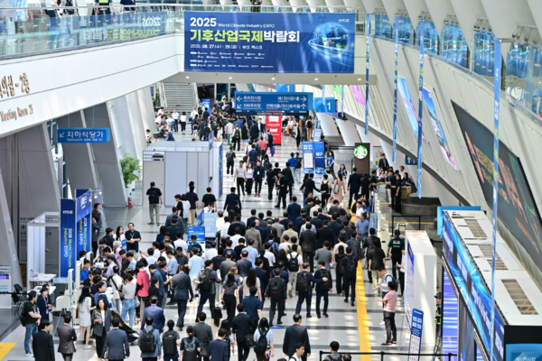
The World Climate Industry Expo (WCE) is Korea's leading international exhibition for the climate and energy sectors and has been held for four consecutive years since its launch. It takes place at BEXCO in Busan in late summer each year.
The World Climate Industry Expo (WCE) is Korea's leading international exhibition for the climate and energy sectors and has been held for four consecutive years since its launch. It takes place at BEXCO in Busan in late summer each year.
Samsung Electronics, LG Electronics, SK Innovation, LS Cable & System and LS Marine Solution unveiled power and energy technologies aimed at addressing the expansion of artificial intelligence (AI) and the energy transition.
The companies are participating in the 2026 World Climate Industry Expo (WCE), held at BEXCO in Busan from Sept. 16 to Sept. 18.
Samsung Electronics and LG Electronics showcased heat pumps and high-efficiency appliances, while SK Innovation presented integrated power solutions for AI data centers. LS Cable & System and LS Marine Solution displayed power grid technologies for transmitting large amounts of electricity.
Samsung Electronics unveiled its "EHS All-in-One" heat pump, which provides cooling, heating and hot water with a single outdoor unit. The company also displayed AI data center cooling solutions developed in collaboration with FläktGroup, which it acquired last year, as well as central heating, ventilation and air conditioning (HVAC) products for large buildings. It also introduced SmartThings-based energy management technology and appliances with the highest energy-efficiency rating.
LG Electronics showcased high-efficiency residential solutions centered on its air-source "LG Therma V Heat Pump Boiler." The product generates about four to five times as much thermal energy as the electricity it consumes. LG Electronics also displayed air conditioners and washer-dryers incorporating heat pump technology, as well as an e-paper display that consumes more than 99% less power than conventional digital signage.
SK Innovation unveiled an integrated energy solution for large-scale electricity consumers including AI data centers. The solution combines renewable energy, battery energy storage systems (BESS), small modular reactors (SMRs) and liquefied natural gas (LNG) combined heat and power generation based on customers' electricity demand. SK Innovation had secured a global renewable energy pipeline of about 5.3 gigawatts (GW) as of the end of May this year.
LS Cable & System and LS Marine Solution introduced a "one-stop integrated power grid" connecting renewable energy generation sites with electricity consumers. They displayed submarine cables that transmit electricity generated by offshore wind farms to land and superconducting cables for high-capacity power transmission. LS Cable & System has commercialized 500-kilovolt (kV) high-voltage direct current (HVDC) cable technology, while LS Marine Solution has experience installing HVDC submarine cables.
LS Cable & System also unveiled recyclable polypropylene (PP) cables and "CuFlake," a new copper material for copper foil made from copper scrap. The company also introduced resource-circulation technology that recycles cross-linked polyethylene (XLPE) insulation from discarded cables.
Electronics and energy companies are expanding related businesses in response to rising power demand driven by the growth of the AI industry and the energy transition. Samsung Electronics and LG Electronics are focusing on reducing energy consumption in homes and buildings, while SK Innovation is targeting power generation and storage, and LS Cable & System and LS Marine Solution are focusing on transmission infrastructure.
Rebellions said on Sept. 16 it will supply racks to Japanese artificial intelligence (AI) company ai&’s data center. The company plans to expand the supply to more than 100 units.
Rebellions will deploy its heterogeneous infrastructure system “REBELRack” at ai&’s data center. An initial batch will be installed at ai&’s Tokyo data center, with additional units to follow. Rebellions declined to disclose the volume or contract value, citing a nondisclosure agreement (NDA) with the customer.
Heterogeneous infrastructure combines different computing devices, including neural processing units (NPUs), graphics processing units (GPUs) and central processing units (CPUs). Rebellions will provide ai&’s data center with a heterogeneous infrastructure solution focused on power efficiency and lower operating costs.
REBELRack is Rebellions’ fully integrated rack-scale AI infrastructure. It supports the open-source frameworks used by ai&, allowing the system to be deployed without a large-scale infrastructure transition. Rebellions expects the system to begin operating at ai&’s data center on the day of delivery.
The system supports up to 32 Rebellions accelerator cards and eight AMD EPYC 9355 CPUs. It has 6 terabytes of DDR5 system memory and delivers 64 petaflops (PFLOPS) of performance using 8-bit floating-point (FP8) operations.
Rebellions said a configuration of 100 REBELRack units would have maximum power consumption of 2.8 megawatts (MW) for the rack equipment alone. The company did not disclose when delivery of all 100 units would be completed. ai& plans to build out its data center to a capacity of 40 MW by the end of 2027.
SK hynix workers approved a revised 2026 wage and collective bargaining agreement in a union vote, three weeks after the first tentative agreement was rejected by a margin of 25 votes. The deal was reached after raising the cash portion of performance bonuses to 50%.
The revised agreement was approved with 8,731 votes, or 57.08%, in a two-day vote held by SK hynix's Icheon and Cheongju union from Sept. 15, according to results released Sept. 16. Of 16,039 eligible members, 15,297 voted, for a turnout of 95.37%.
The basic payout ratio for the company's profit-sharing (PS) bonus was adjusted to 50% cash and 50% stock. The first agreement called for 40% in cash and 60% in stock. The revised deal also gives employees the option to convert the cash portion into stock in increments of 10 percentage points.
Deferred portions of performance bonuses calculated based on last year's results that had been scheduled for payment next year and the following year will also be paid earlier. Single-parent households were added to the eligibility for additional housing loan support, which previously covered married households. The broader framework of the previous agreement, including a 6.3% wage increase and the deferral of a portion of wages in the event of losses, was maintained.
The first tentative agreement was rejected in an all-employee union vote on Aug. 25, with 7,535 votes, or 50.08%, against and 7,510 votes, or 49.92%, in favor. Labor and management then held about two weeks of additional negotiations and reached the revised agreement on Sept. 9.
SK hynix and the union will hold a signing ceremony for the final agreement before the Chuseok holiday, completing this year's wage and collective bargaining process.
"We thank the labor union and our employees for working with us through this difficult process," SK hynix said. "We will continue to work together as a company and employees to address and overcome the challenges we face."
Wonik Robotics is seeking to supply humanoid robots to Samsung Electronics' semiconductor plants.
"We are currently conducting proof-of-concept (PoC) testing of wheeled robots with Samsung Electronics and other major semiconductor companies," Wonik Robotics Executive Director Kim Min-cheol said at the Korea Semiconductor Industry Association's Advanced Sensor Forum held at Josun Palace in Seoul's Gangnam district on Sept. 15.
Samsung Electronics' evaluation consists of three stages. It first checks whether the robot operates properly and then evaluates its reliability. During reliability testing, Samsung examines whether the robot can handle variables that may arise when handling wafers, including minute vibrations and dust. Semiconductor plants are highly sensitive to vibration and dust, creating a high barrier to the adoption of humanoid robots.
Even if the robot passes Samsung Electronics' final evaluation, the initial supply volume is expected to be limited. "If we pass, it will be meaningful in that we will have secured a major corporate customer," Kim said. He did not disclose the expected supply volume or timing.
Wonik Robotics' robot is wheeled. Humanoid robots can be divided into wheeled and bipedal types based on their method of locomotion. Wheeled robots have a human-like upper body but use wheels instead of legs for their lower body.
The robot is designed to transport wafers and other materials inside semiconductor plants, replacing tasks currently performed by workers. Wonik Robotics has previously supplied robotic hands for automation at Samsung Electronics' smartphone inspection lines.
Wonik Robotics develops the robot's body, including its hands, arms and lower body, in-house. The company is considering eventually supplying only the robotic hands while sourcing the remaining components externally. Robotic hands are one of the biggest technological bottlenecks in humanoid robots because they require the most precise movements. They are also among the most expensive robot components.
Wonik Robotics uses a five-finger robotic hand modeled after the human hand. The company also considered a four-finger design excluding the little finger, but opted for five fingers to ensure a stable grip on objects.
A key technology in the robotic hand is artificial intelligence (AI)-based object recognition. Sensors embedded in the hand detect an object's type, material and weight. The robot adjusts its grip strength accordingly, applying more force to heavier objects and less to fragile ones. AI assists in recognizing objects. Wonik Robotics develops its AI models in-house and uses proprietary data accumulated over more than a decade in the robotic hand business to train them.
Wonik Robotics' new plant in Wanju, North Jeolla Province, is expected to serve as its mass-production base for robots. The company has its headquarters in Seongnam and a research center in Anyang, both in Gyeonggi Province. Last month, Wonik Robotics said it would secure 350 billion won in funding from the government for projects including construction of a robotic hand production plant in Wanju.
HS Hyosung Information Systems, an AI and data infrastructure solutions provider, held its Data Center Modernization Conference 2026 at Lotte Hotel Busan on Sept. 15. The conference is an annual event that HS Hyosung Information Systems has held for IT professionals in the Busan and South Gyeongsang region for more than a decade.
HS Hyosung Information Systems said it shared strategies and insights for data center modernization in the AI era, including data and infrastructure strategies for enterprise AI, more efficient private cloud operations and ways to strengthen cyber resilience.
According to HS Hyosung Information Systems, data center infrastructure is increasingly required to reliably process and operate large-scale AI workloads and vast amounts of data, driving a shift toward redesigning overall infrastructure to integrate AI infrastructure, cloud operations and data protection.
In response to these changes, the conference broadly covered key infrastructure strategies required for data centers, including data and infrastructure development for enterprise AI, modernization of AI training and inference environments, greater efficiency in private cloud and data center operations, and security and data protection.
Dong-soo Kwon, a senior expert at HS Hyosung Information Systems, delivered a keynote presentation titled "Data and Infrastructure Strategies for Enterprise AI in the Agentic AI Era of 2026." Go-hoon Jung, a project manager at HS Hyosung Information Systems, then outlined the company's capabilities and strategies for building private clouds through a smart city development project case study. Dong-hyuk Kim, a team leader at HS Hyosung Information Systems, also presented data protection and recovery strategies designed to support uninterrupted business operations amid disasters and cyber threats.
Major technology partners also participated. FuriosaAI showcased its RNGD neural processing unit (NPU), which supports high power efficiency and high-performance inference, while Lablup presented modernization tools for efficient AI training and inference.
VMware by Broadcom shared ways to reduce data center costs using VMware Cloud Foundation (VCF), while Veeam Software presented next-generation service recovery strategies for zero-trust environments. Palo Alto Networks Korea presented a data center modernization strategy using its Precision AI-based security platform.
The venue also featured exhibition booths where attendees could explore technologies and solutions from major partners including C Platform, Ocean Technology, Gensys and Union Biometrics.
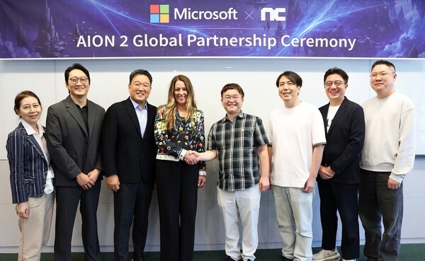
From left, Microsoft Korea Technical Sales Manager Lee Jong-hee, Gaming Customer Business Sales Representative Ma Seung-jae, CEO Cho Won-woo, Microsoft Executive Vice President and Chief Revenue Officer for Global Enterprise Deb Cupp, NC CBO Baek Seung-wook, AION 2 Global Publishing Head So In-seop, IP Alliance Director Choi Won-jong and AION 2 Technical Director Pung Hyun-seop. (Photo: NC)
From left, Microsoft Korea Technical Sales Manager Lee Jong-hee, Gaming Customer Business Sales Representative Ma Seung-jae, CEO Cho Won-woo, Microsoft Executive Vice President and Chief Revenue Officer for Global Enterprise Deb Cupp, NC CBO Baek Seung-wook, AION 2 Global Publishing Head So In-seop, IP Alliance Director Choi Won-jong and AION 2 Technical Director Pung Hyun-seop. (Photo: NC)
NC is working with Microsoft to prepare for the global launch of its new game “AION 2,” with Microsoft Korea setting up a dedicated team for the title. The companies will build global service infrastructure based on Microsoft Azure and pursue joint marketing with Microsoft’s global gaming organization.
NC said on Sept. 15 that it is strengthening its strategic partnership with Microsoft Korea to support the global service of AION 2.
Executives from the two companies met at NC’s R&D Center in Pangyo, Seongnam, on Sept. 14 to discuss cooperation for the global launch and operation of AION 2. Participants included NC Chief Business Officer (CBO) Baek Seung-wook and Microsoft Korea Chief Executive Officer Cho Won-woo.
Ahead of AION 2’s global launch on Oct. 5, NC will use Microsoft Azure’s global infrastructure. The aim is to handle large numbers of simultaneous users and regional traffic fluctuations during the global launch.
Microsoft plans to deploy its global technical organization and a dedicated Korea team to support AION 2, from performance verification before launch to incident response after the service goes live.
The companies will also expand their marketing partnership. They plan to conduct joint marketing with Microsoft’s global gaming organization to broaden AION 2’s reach among global users. Specific marketing methods and channels were not disclosed.
The partnership between NC and Microsoft also extends beyond game services. NC has deployed Microsoft 365 E5 companywide to establish its security and collaboration environment and is considering using Microsoft 365 Copilot to improve employee productivity.
“Microsoft, with its global operational capabilities and technical expertise, is a key partner joining NC in our most important global challenge,” Baek said.
“Microsoft will support NC’s service operations with its cloud capabilities and engineering expertise and work together to provide a stable gaming experience for users worldwide,” Cho said.

 Login