 Login
OpenAI Targets Models for Chip Design as Enterprise Revenue Climbs
9 September 2026 at 12:56
OpenAI Goes After Industry Verticals OpenAI is steering its models into specialised industries and undercutting open-source rivals on


For more than a decade, scientists have known that strange bacteria living in aquatic mud can conduct electricity along distances thousands of times longer than a single bacterial cell. Such long-range electrical conduction should be extraordinarily difficult for a living organism, and how they accomplish the feat has remained a biological mystery.
Now, researchers say they have found the wiring. Inside so-called cable bacteria, scientists have discovered an elaborate network of nickel-rich nanoribbons arranged into what amounts to a naturally grown electrical cable.
The structure is unlike the conventional machinery biology normally uses to move electrons and may represent the first known example of a metal-organic framework produced by a living organism.
What surprised lead study author Dr. Filip Meysman, a professor at the University of Antwerp in Belgium, most was not how alien the structure looked, but how familiar it was.
“It had a very familiar feeling: a braided wire consisting of thin individual wires surrounded by a protective shell layer,” Meysman told The Debrief. “This is very similar to the power cords that we use to charge our smartphones, only the cable bacterial version is 20,000 times smaller in size. Evolution came up with this design 600 million years earlier than electrical engineers.”
Meysman’s comparison is not simply rhetorical. Molecular-clock estimates suggest the cable bacteria lineage may have diverged roughly 560 million years ago, although when their unusual electrical capabilities evolved is still unknown.
Published in Nature Communications, the findings could eventually provide researchers with a biological blueprint for creating flexible, biodegradable electronics that organisms effectively manufacture themselves.
Cable bacteria first attracted scientific attention because of their outstanding ability to move electrons over centimeter-scale distances. The multicellular organisms live in sediments where different layers offer different chemical resources. Cells buried deeper can harvest electrons from sulfide, while cells closer to oxygen-rich water dispose of them.
The result is an organism that successfully separates parts of its metabolism across space, with electrical current passing along the filament connecting them.
Scientists eventually identified dozens of parallel fibers running through the bacteria’s outer layers as the likely electrical pathways. Measurements later showed conductivity reaching levels unusual for any biological material and, in some experiments, comparable to materials used in electronic inks. The new study notes previously reported conductivity values reaching up to 500 siemens per centimeter.
But knowing where the current traveled was not the same as knowing how it traveled.
Most biological electron conduction relies on proteins containing metal-bearing cofactors, commonly iron-containing structures such as hemes or iron-sulfur clusters. Electrons typically move between those sites in a sequence of molecular transfers often described as “hopping.”
Previous research showed that cable bacteria did not fit neatly into that model. Their conducting fibers were associated with sulfur-bound nickel rather than the usual iron cofactors. At the same time, theoretical work suggested electron movement was too fast to be explained by conventional non-adiabatic hopping alone.
The mystery deepened in 2024, when some of the same researchers examined cable bacteria at temperatures approaching that of liquid helium and found that their electrical behavior matched an unusually efficient multistep hopping mechanism. But even then, the extraordinary conductivity challenged standard models of electrons simply hopping between isolated molecular sites.
The new structural work may help explain why.
Rather than a series of small, separated metal cofactors, the researchers have now found an extended nickel-organic structure running through the conductive fibers.
Using electron microscopy, X-ray fluorescence, Raman spectroscopy, electron paramagnetic resonance, X-ray absorption spectroscopy, and computer modeling, the team found that each conductive fiber contains roughly 11 extraordinarily thin nanoribbons, about 1.4 nanometers across.
Those ribbons pass through the center of the fiber and are built from repeating nickel bis-dithiolene complexes, which the researchers call NiBiD. Nickel atoms are linked through sulfur-containing organic molecules, creating planar units that appear to stack into an extended, highly ordered electrical pathway.
That arrangement may explain the extraordinary conductivity. Rather than electrons simply jumping between isolated metal centers, the stacked structure creates extensive electronic interaction and delocalization, allowing charge to spread across overlapping molecular networks. In that sense, the bacterial wire begins to resemble an organic electronic material more than a conventional biological electron-transfer chain.
The arrangement also appears mechanically well-suited to the bacteria’s lifestyle.
Cable bacteria move through sediment and can bend sharply while maintaining electrical contact between cells. A single rigid conducting strand could be vulnerable to damage. Multiple intertwined nanoribbons, however, offer something closer to braided copper wire: strength, flexibility, and redundancy at the same time.
The discovery also appears to broaden scientists’ understanding of what biology can manufacture.
Metal-organic frameworks, or MOFs, are structures in which organic molecules link together metal centers into larger networks. Chemists have spent years designing them for uses ranging from gas storage and chemical separation to catalysis and electronics.
Until now, the researchers say, no one had observed a metal-organic framework configuration naturally constructed inside a living organism.
Cable bacteria appear to have arrived at the idea on their own, and this natural version appears to conduct electricity exceptionally well.
Previous electrical conductivity measurements of cable bacteria used the entire cross-section of their conductive fibers. But the new structural work indicates that the current is concentrated within a much smaller network of nanoribbons.
Recalculating conductivity based on the estimated dimensions of those conducting channels, the researchers found that an individual nanoribbon could have a conductivity of roughly 150 to 15,000 siemens per centimeter.
That range, the researchers say, ranks among the highest reported for any metal-organic structure. The upper figure remains an estimate, however, instead of a direct measurement of a single nanoribbon.
“We need to be able to isolate the individual nanoribbons from the cable bacteria and connect them electrically with electrodes,” Dr. Meysman explained. “This would provide the direct proof of the high conductivity. We are currently working on such nanoscale electrical measurements.”
Doing so would let researchers determine whether the extraordinary conductivity predicted for an individual nanoribbon holds up experimentally.
If it does, the technological implications could extend well beyond understanding an unusual microbe.
Researchers have long been interested in bio-based electronics because living systems can manufacture sophisticated materials through self-assembly while operating under relatively mild conditions. Biological materials can also be flexible and potentially biodegradable.
Their weakness has usually been electrical performance. Cable bacteria suggest nature may have found a way around that tradeoff.
Scientists still do not know exactly how cable bacteria biosynthesize the nickel-organic framework, and parts of the nanoribbon architecture remain unresolved.
But evolution has already solved one problem materials scientists would like to reproduce: how to build a highly conductive, flexible electrical pathway largely from organic components under biological conditions.
Dr. Meysman says one especially promising possibility is flexible printed electronics, where conductive inks are deposited onto surfaces to create circuits, sensors, and other electronic components.
“The material produced by the bacteria provides a flexible and conductive material, and so flexible printed electronics—conductive inks—emerges as a promising application domain,” Dr. Meysman said.
“The challenge is to demonstrate that the biomaterial can be made in a cost-effective fashion,” Meysman added, “and that it has the same—or even better—properties than the electronic ink materials currently in use.”
Ultimately, for hundreds of millions of years, bacteria buried in mud may have been growing microscopic power cables.
Scientists are only now beginning to understand how they work.
The study, “Highly efficient long-range conduction through a biosynthetic nickel-organic framework,” appeared in Nature Communications.
Tim McMillan is a retired law enforcement executive, investigative reporter and co-founder of The Debrief. His writing typically focuses on defense, national security, the Intelligence Community and topics related to psychology. You can follow Tim on Twitter: @LtTimMcMillan. Tim can be reached by email: tim@thedebrief.org or through encrypted email: LtTimMcMillan@protonmail.com
Leading chipmakers Samsung Electronics and Taiwan Semiconductor Manufacturing Co. announced plans to adopt ASML’s latest chipmaking machines in the next several years—and they also joined Intel in agreeing to a crucial technology change that could boost chip production on the new machines by 40 percent.
This signifies the semiconductor industry’s broader embrace of high NA EUV photolithography technology that can cost up to $400 million per machine and is only provided by the Dutch technology company ASML, Bloomberg reports. The technology would allow chip designers to implement even smaller features in potentially more powerful and efficient next-generation chips produced for AI data centers and consumer electronics such as smartphones, tablets, and laptops.
ASML’s EUV (extreme ultraviolet) lithography machines enable chipmakers to use powerful laser light to imprint patterns in silicon wafers, layer by layer, and gradually form the computer circuitry that makes silicon chips work. Compared to older deep ultraviolet lithography, EUV technology harnesses a more powerful source of light with a shorter wavelength to create even smaller features on silicon wafers.

© Michel de Heer | ASML
Leading chipmakers Samsung Electronics and Taiwan Semiconductor Manufacturing Co. announced plans to adopt ASML’s latest chipmaking machines in the next several years—and they also joined Intel in agreeing to a crucial technology change that could boost chip production on the new machines by 40 percent.
This signifies the semiconductor industry’s broader embrace of high NA EUV photolithography technology that can cost up to $400 million per machine and is only provided by the Dutch technology company ASML, Bloomberg reports. The technology would allow chip designers to implement even smaller features in potentially more powerful and efficient next-generation chips produced for AI data centers and consumer electronics such as smartphones, tablets, and laptops.
ASML’s EUV (extreme ultraviolet) lithography machines enable chipmakers to use powerful laser light to imprint patterns in silicon wafers, layer by layer, and gradually form the computer circuitry that makes silicon chips work. Compared to older deep ultraviolet lithography, EUV technology harnesses a more powerful source of light with a shorter wavelength to create even smaller features on silicon wafers.
© Michel de Heer | ASML
© DARPA
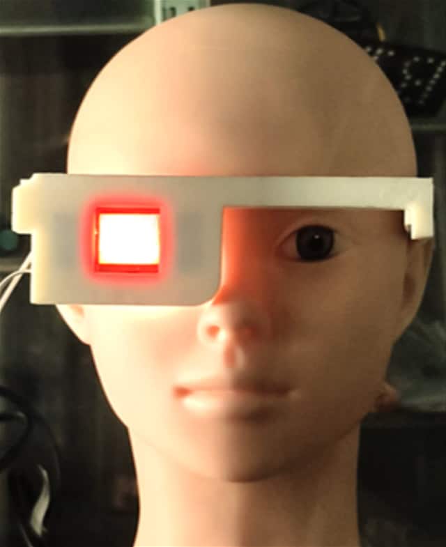
Most people can perceive different colours in the visible range of the electromagnetic spectrum – at wavelengths between about 400 and 700 nm. However, our eyes cannot see infrared radiation, let alone perceive infrared “colours”. But now a team at China’s Beijing Institute of Technology has created colloidal quantum dot-based light upconverters that convert the infrared to the visible while preserving the spectral notion of colour. These nanostructures can be incorporated into wearable eyeglasses and, more ambitiously, could someday be implanted directly into the retina.
Photoreceptors in mammalian eyes contain light-absorbing pigments consisting of opsins and their covalently linked retinals. Infrared light at wavelengths greater than 700 nm cannot be absorbed by these photoreceptors, so when such light reaches the retina no corresponding electric signal is sent to the brain. Seeing infrared radiation could reveal otherwise invisible features and improve night vision, which relies on infrared light.
In recent years, researchers have made great strides in developing materials that capture photons with lower energies (in the infrared, for example) and re-emit them as photons with higher energies (typically visible or ultraviolet light). This process is known as upconversion, and the emitted light is said to be anti-Stokes shifted. This has led to the development of photoreceptor-binding upconversion nanoparticles that convert infrared light into visible emissions. These have been injected into mouse eyes and have been used to create wearable lenses for humans – with nonlinear upconversion projecting infrared-transformed visible light onto the cornea. While effective, these applications are limited to the narrow near-infrared (NIR) spectral range.
Now, a team led by Ge Mu and Xin Tang studied a structure made up of semiconducting mercury telluride (HgTe) colloidal quantum dots (CQDs) atop an organic light-emitting diode (OLED). The OLED contains two light-emitting layers, one red-light-emitting and one cyan-light-emitting. Because of the small size of the CQDs, the electrons in them are confined in all three directions. This means that the electrons are restricted to discrete and separate atomic-like energy subbands rather than having access to a continuous band of allowed energies as they would in a bulk material.
When the CQDs absorb photons with infrared wavelengths, spanning the NIR to short-wave infrared regions, they produce excited carriers (electrons and holes) that then travel from their different energy levels into the OLED. This is a seamless process because the OLED is designed so that its electronic bands align with the sub-bands of the HgTe. When either the light intensity or the wavelength of the incident infrared light changes, explains Tang, the excited photocarriers are transported and recombined in the different emissive layers of the OLED thanks to the hole-trapping barriers that were engineered in these layers. The result is infrared-to-visible-light (red and cyan) upconversion.
As a proof-of-concept, the researchers integrated their upconverter into lightweight, semi-transparent wearable eyeglasses and found that they can project multispectral infrared light onto the retina without affecting normal vision, so allowing the wearer to see infrared light as well as visible light. Indeed, a wearer can detect infrared light at wavelengths greater than 2 μm with a luminance of over 700 cd m−2.
Looking ahead, Tang says that the upconverter could be bound to light-sensitive proteins in the retina and so serve as an implantable next-generation retinal bionic photoreceptor. This structure would transform infrared light into visible light emissions that stimulate light-sensitive proteins on retinal neurons to bypass damaged photoreceptor cells and potentially restore visual function across both the visible and infrared.
This full colour upconverter has been a long-term project in my group, Tang tells Physics World. “Starting from an efficient single-colour upconverter, we then successfully demonstrated colour-tuneable OLEDs and Si-/Ge-/CMOS-integrated upconverters. And with our recent progress on the understanding of interfacial carrier transport between quantum dots and colour-tuneable OLEDs, we have now demonstrated this new full-colour upconverter.”
The latest work is detailed in Science Advances.
The post Upconverting colloidal quantum dots bring ‘colour vision’ to the infrared appeared first on Physics World.
Researchers at Kyushu University in Japan have developed a flexible electronic circuit that can connect itself to another electronic circuit and then disconnect from it. The prototype structure is an important step towards electronic devices that can reconfigure and even repair themselves, and it could have applications in wearable sensors, soft robotics and medical devices.
Most of today’s electronic devices are fixed, or “non-modular”, explains study leader Fumihiro Sassa of Kyushu University’s Department of Electrical and Electronic Engineering. Typically designed for specific tasks or environments, they are not readily adaptable to new ones, and they often cease to function if even a single component in their electronic circuitry fails. This leaves them dependent on human operators or external robotic systems if it becomes necessary to expand their functionality or repair damage.
“This can be a serious limitation inside very small machines, in space equipment, in devices requiring specialized handling, such as wearable chemical sensors, or in systems containing very large numbers of wires and electronic elements,” Sassa explains. “In such cases, in-situ repair can be difficult. The whole system may need to be replaced.”
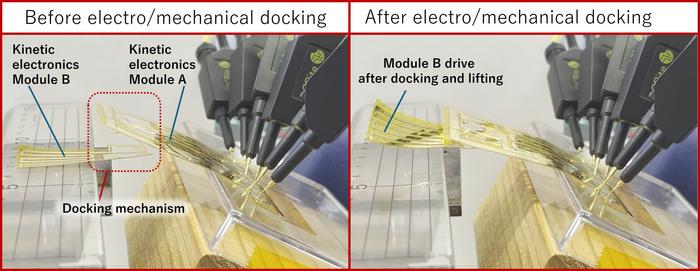
To overcome this problem, the Kyushu University researchers have been developing what they term “kinetic electronics” modules. These consist of electronic circuits and actuators that deform when an electrical current is applied to them so that they can mechanically and electrically connect to other modules. Before this connection takes place, different modules are separate, but after connection or “docking” takes place, one module can independently deform another when power is supplied through the point that connects them.
In this way, explains Sassa, the circuits can rearrange their own hardware structure. “Such functions have traditionally been used in mechanical systems, such as spacecraft, trains and modular robots, but we have now applied them to an electronic device.”
Sassa and colleagues fabricated their electrothermal bimorph actuators from polypropylene and polyimide films with heater electrodes and electrical circuits formed on them through a two-dimensional top-down process. Because the two polymers expand differently, Sassa explains that Joule heating causes selected actuator sections to bend. “Prescribed sequences of these motions produce docking and undocking and once docked, passive mechanical engagement maintains the connection without continuous power being supplied,” he says. “Undocking requires a separate actuation sequence.”
The researchers say they are working on miniaturizing their system and looking how to control it more intelligently. In the present study, which is detailed in npj Flexible Electronics, they demonstrated the docking mechanism using a small number of millimetre-scale independent sensors and actuators formed together on the circuit, with motion being controlled in sequence by an external microcontroller. They are now developing photolithographic processes to further decrease the size of these components and have already fabricated actuators smaller than 100 μm using these techniques.
“In a similar way to large-scale integration in conventional electronics, doing this will allow us to integrate very large numbers of these sensing and actuation elements, allowing the electronic circuit to form and change much more complex mechanical structures and functions,” says Sassa.
“We are also interested in so-called distributed control, in which the central controller does not need to specify every movement,” he adds. “Instead, many elements would follow relatively simple local control rules, from which advanced self-reconfiguration and self-organization could emerge.”
The post ‘Kinetic electronics’ make self-connecting circuits appeared first on Physics World.
