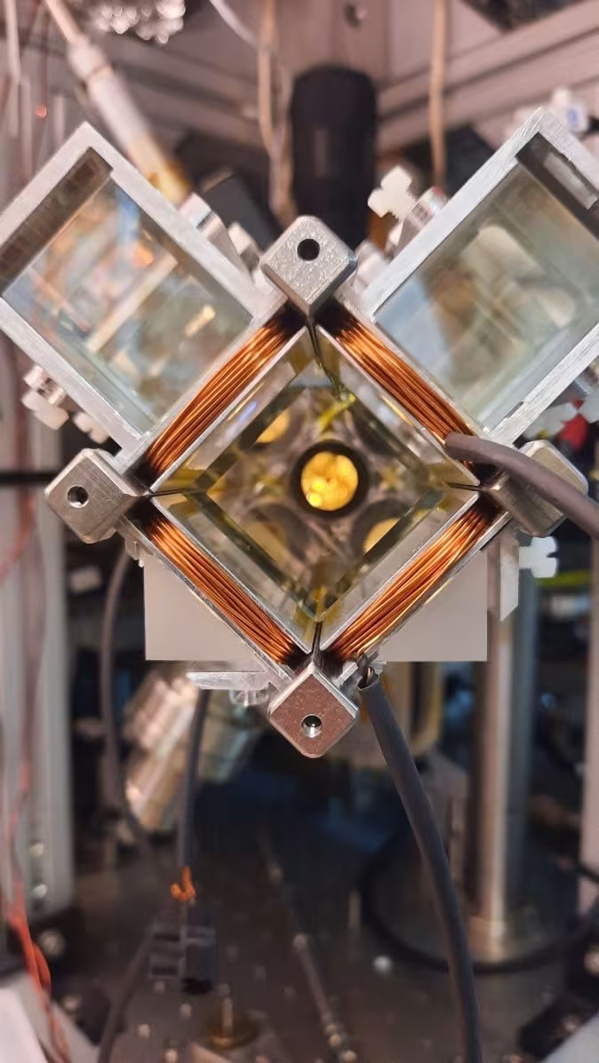
Circular Rydberg atoms set three records, staying stable for 11 milliseconds
Nickel disulfide, NiS₂, is an unusual material. Its interior behaves as an electrical insulator, blocking the flow of current, while certain parts of its surface conduct electricity freely. This contradiction has puzzled physicists for decades, and a recent study offers a detailed explanation. The conduction, it turns out, is confined to tiny one-dimensional steps on the surface, and these narrow conducting channels are a direct consequence of how electrons are arranged inside the crystal.
NiS₂ shares its crystal structure with pyrite, the mineral sometimes called fool’s gold. At ordinary conditions, its electrons do not move freely through the lattice: the strong electrical repulsion between them opens an energy gap that keeps the bulk of the material insulating. This behaviour defines what physicists call a Mott, or charge-transfer, insulator, a category of materials that simple band theory cannot explain. Band theory predicts that any material with a partially filled outer electron shell should conduct electricity, yet compounds like nickel oxide obstinately insulate instead. In 1949, the physicist Nevill Mott showed why: if two electrons crowding the same atomic site cost more energy than is available, the electrons stay locked in place and no current flows, regardless of what band theory predicts. NiS₂ behaves in much the same way.
Yet electrical-transport measurements had repeatedly found that crystals of NiS₂ conduct through their surfaces. Earlier scanning-tunnelling experiments helped explain part of the puzzle: the broad, flat surface remains insulating, but the electronic gap narrows sharply near atomic-scale steps, tiny cliffs just one or two atoms high where the surface abruptly changes level. A new study 1 confirms this picture and examines the steps with much higher spatial resolution than before.
A scanning tunnelling microscope (STM) works by bringing an extremely sharp needle close enough to a surface that electrons can leak across the gap between tip and sample. Measuring that leakage at different energies reveals both the surface’s shape and how easily electrons can enter or leave it. In NiS₂, these measurements uncovered electronic states concentrated tightly along the step edges: the states extend for a long distance parallel to a step but stay confined to roughly one to two nanometres across it. In other words, the electrons are effectively free to move in one direction while remaining trapped in the other two, forming genuine one-dimensional conduction channels.

Two distinct kinds of surface step were observed, depending on whether the outermost atomic layer exposes nickel or sulfur atoms. Both carry electronic states associated with their steps, but they are not equally important. The nickel-terminated steps host states that sit right at the energy where electrical conduction happens, making them the most likely explanation for the surface conductivity that transport experiments had measured for years. The sulfur-terminated steps also host states inside the insulating gap, but their energy is positioned further away, making them less directly responsible for carrying current.
The study also tested what happens when a magnetic field is applied perpendicular to the surface. The step-edge states survived fields as strong as 10 tesla, a field far stronger than any produced by a laboratory magnet used for everyday purposes. Their intensity weakened somewhat, particularly on the sulfur-terminated steps, but the states were never destroyed. This robustness matters because NiS₂ already displays complicated magnetic behaviour of its own, which might easily have disrupted a more fragile conducting state.
The deeper explanation lies in how electrons are distributed inside the crystal. In an ordinary insulator, the occupied electronic states can usually be pictured as clouds centred on the atoms themselves. NiS₂ is different: calculations show that part of its electron density is naturally centred at special positions between atoms, specifically near the midpoints of pairs of sulfur atoms, where no atom actually sits. Physicists call these obstructed charge centres, and materials built around them belong to a class known as obstructed atomic insulators, a concept that grew out of a broader effort over the past decade to classify materials by the geometry, and not just the energy, of their electron states.

This arrangement is not a chemical accident; it is protected by the symmetry of the crystal. When the crystal is cut to form a surface, though, the special positions that hosted this electron density can no longer fit together the way they did in the bulk. At a step edge, this mismatch creates what is known as a filling anomaly: an imbalance in how the available electronic states can be occupied, which leaves behind a state inside the insulating gap, localized right at the edge. Calculations of artificial step structures reproduce the main features seen under the microscope, including this localization, supporting the idea that the conducting channels are not ordinary metallic defects caused by broken chemical bonds, but a direct consequence of the crystal’s underlying electronic geometry.
The study also settles a long-standing question about NiS₂’s magnetism at low temperature. Below about 39 kelvin, the nickel magnetic moments arrange themselves into a non-collinear antiferromagnetic pattern, with neighbouring moments pointing in different directions that largely cancel out. Below about 30 kelvin, they rearrange again into a state that produces a small but measurable net magnetization. New neutron-diffraction measurements support a revised model of this low-temperature arrangement, resolving a debate about the material’s magnetic ground state that had lasted for roughly fifty years.
Taken together, the results give NiS₂ a significance well beyond its peculiar conducting surface. The material shows that strong repulsion between electrons, magnetism, and the geometry of electronic states can coexist within a single crystal. Such geometric protection is normally associated with topological materials, in which certain electronic states are shielded from disorder or defects by the crystal’s symmetry. The new results suggest that this protection can survive even when strong interactions push a material into being an insulator, making NiS₂ a rare setting for studying how the quantum-mechanical arrangement of electrons decides where electricity is allowed to flow within an otherwise insulating crystal.
Author: César Tomé López is a science writer and the editor of Mapping Ignorance
Disclaimer: Parts of this article may have been copied verbatim or almost verbatim from the referenced research paper/s.
The post Why an insulator can conduct electricity along its edges appeared first on Mapping Ignorance.

For the first time, physicists have measured the tiny quantum shift an object acquires by falling through Earth's gravity — an effect of Einstein's relativity that was predicted almost a century ago but never observed.
Researchers placed ultracold rubidium atoms into a superposition, a quantum state in which a single particle takes two paths at once. In this experiment, one path put the atom in free fall while the other kept it motionless. Recombining the atoms revealed an almost imperceptible difference between the two paths.
The measurement, published Sept. 2 in the journal Science Advances, shows that Einstein's equivalence principle — the idea at the heart of general relativity — still holds when it is pushed into the quantum world, creating a small but tantalizing link between relativity and quantum mechanics.
"The principle says that acceleration and gravity cannot be distinguished locally," Vlatko Vedral, a physicist at the University of Oxford and a co-author of the new study, told Live Science via email.
The classic illustration of the equivalence principle is a thought experiment known as Einstein's elevator. A person sealed in a windowless elevator cannot tell whether the floor is pressing against their feet because the elevator is parked motionless on Earth or because it is being accelerated through empty space. Einstein called that realization the "happiest thought" of his life and built general relativity around it.
For heavy, everyday objects, the equivalence principle has been tested to extraordinary precision. Quantum objects are a different matter. They behave like waves, and each wave carries a quantity called phase — essentially, where its crests and troughs sit. Phase cannot be seen directly, but when two versions of the same particle are recombined, any mismatch between their phases shows up as an interference pattern. The two waves reinforce each other in some places and cancel each other out in others, thereby changing the odds of where the particle turns up.
Theory says that a wave in free fall should build up phase relative to an identical wave held still and that this phase should grow with the cube of the falling time. Therefore, doubling the fall time multiplies the effect eightfold. Charles Galton Darwin, a grandson of the famous naturalist, and Earle Kennard both documented this prediction in 1927 — but no one had measured it until now.
Catching the effect required an instrument with one arm genuinely at rest with respect to Earth and the other in genuine free fall — something no previous experiment could supply. Matter-wave experiments going back to the neutron interferometry of the 1970s had measured gravity in other ways, but never with that pair of trajectories.
The team behind the new study, led by physicist Ron Folman at Ben-Gurion University of the Negev in Israel, chilled roughly 20,000 rubidium atoms into an exotic state of matter called a Bose-Einstein condensate, released them from their magnetic trap and ran the interferometer about 113 micrometers beneath an "atom chip" patterned with gold wires only 2 micrometers thick.
Radio and microwave pulses put each atom into a superposition of two magnetic states. A magnetic kick launched one of them upward, and a fraction of a millisecond later, a second pulse made that half insensitive to magnetic fields so that it rose and fell under gravity alone. The other half remained magnetically sensitive and felt a force tuned to cancel gravity exactly, leaving it suspended in place.
At the top of the arc, the two halves of a single atom stood about 7.5 micrometers apart — about seven times the width of the atomic wave itself — before the sequence was reversed to bring them back together. The team named the device the quantum Galileo interferometer, after the scientist who first argued that all objects fall at the same rate.
"Two different accelerations can be superposed, zero [acceleration] and the Earth's gravitational acceleration, and the resulting quantum interference measured," Vedral said.
The researchers tracked the interference signal as they stretched the free-fall time to about 2.4 milliseconds. Across 633 runs over 5.3 hours, they recorded 13 complete oscillations, each one a full cycle of phase built up between the two halves of the atom. The growth followed the cube of the falling time, matching the theoretical model to within about 2.5%.
"The phase between the two elements of the superposition, which grows as the cube of the duration of the experiment and which was predicted a long time ago, in 1927, has now finally been observed for the first time," Vedral said.
The result matters because the same phase can be derived in two completely different ways: One treats gravity as a force acting on a quantum wave; the other moves into the falling frame, where gravity vanishes, and invokes the equivalence principle. Both give the same answer, and that agreement is what allows quantum mechanics and general relativity to coexist.
"They tell us that, at this level of accuracy, there is no conflict between quantum physics and gravity," Vedral said. "In other words, the equivalence principle is perfectly compliant with quantum mechanics."
The hardest part of the experiment was the recombination. Because the two halves of the atom end up moving at very different speeds, returning them to overlap in both position and motion is extremely demanding. Physicists Marlan Scully, Berthold-Georg Englert and Julian Schwinger named the problem the "Humpty-Dumpty effect." The magnetic fields also curve across the atom cloud, distorting the two halves in different ways.
The contrast of the interference fringes started at 80% for short runs and faded to 20% for the longest run, setting a practical ceiling on how long the experiment can run. The authors also cautioned that their measurement does not rule out every theory in which the equivalence principle breaks down, because some of those theories predict the same phase.
The team now wants to test the equivalence principle under more general conditions, such as the "same experiment in a rotating frame," Vedral said. "Even more interestingly, performing an experiment in which two such systems are superposed and can gravitationally affect one another" would further test the results, he added.
That last idea points toward one of the field's central open questions. Scaling up the technique from atoms to far heavier objects, such as nanodiamonds, would let physicists ask whether gravity itself follows quantum rules and would open a route to testing the conjecture — championed by study co-author and Nobel laureate Roger Penrose — that gravity is what destroys quantum superpositions in the first place.
See how much you know about Albert Einstein with our Albert Einstein quiz!
A material that normally blocks the flow of electricity can suddenly begin behaving like a metal when exposed to remarkably weak light, according to a new experiment involving one of the strangest forms of graphene ever created. The breakthrough reveals that an unusual quantum effect could eventually provide a new way to detect some of the faintest radiation around us.
Researchers working with “magic-angle” twisted bilayer graphene found that faint, long-wavelength radiation can effectively melt the material’s fragile correlated insulating state, causing its electrical resistance to plummet. Remarkably, the experiments showed that even relatively weak radiation could trigger a dramatic transition from an insulator to a metal.
Beyond revealing an unusual way that light can manipulate matter, the discovery could provide the foundation for extremely sensitive detectors capable of spotting faint terahertz and far-infrared radiation.
With further development, detectors operating at these wavelengths could have applications ranging from security imaging and material inspection to astronomy and environmental sensing.
The study, published in Nature Communications, centers on magic-angle twisted bilayer graphene, or MATBG—a material produced by stacking two sheets of graphene and rotating them relative to one another at a carefully controlled angle.
Under the right conditions, interactions between electrons can cause magic-angle graphene to enter exotic collective states, including superconducting and insulating phases.
“Here we show that this expectation does not apply to magic-angle twisted bilayer graphene (MATBG) and demonstrate giant photoresponse of MATBG to low-intensity long-wavelength photons when it is tuned to half filling of the moiré band,” researchers write. “Far-infrared photons selectively overheat the low-heat-capacity electronic subsystem, driving a collapse of the correlated order and producing a giant photoresistive response.”
Ordinarily, changing an insulator into a conductor with light requires supplying enough energy to alter how electrons can move through the material fundamentally. Previous experiments involving light-induced insulator-to-metal transitions have frequently depended on intense, ultrafast excitation.
Magic-angle graphene offers another route.
Twisting graphene sheets at carefully controlled angles creates a larger repeating structure known as a moiré superlattice, dramatically changing how electrons within the material interact. Those interactions have already produced some remarkable results.
As The Debrief reported last year, researchers studying magic-angle twisted trilayer graphene uncovered new evidence of unconventional superconductivity, including unusually tightly bound electron pairs and a distinctive superconducting energy gap.
That work was part of a greater effort to understand whether these exotic materials could eventually help scientists design superconductors capable of operating at much higher temperatures.
In the new study, researchers exploited another unusual state that can emerge in magic-angle graphene. At certain electron densities, interactions between electrons become unusually important, allowing them to organize into what physicists call a “correlated insulator.”
That collective state is extremely fragile. The correlated insulating gap exists at an energy scale of only a few millielectronvolts. Previous measurements cited by the researchers indicate that a gap of approximately 1 millielectronvolt at very low temperatures gradually closes as the material warms and disappears around 10 kelvin.
The researchers realized that weakness could become an advantage.
Their experimental device consisted of magic-angle graphene sandwiched between layers of hexagonal boron nitride and configured as a field-effect transistor. A graphite back gate allowed them to precisely control the number of charge carriers and tune the graphene into its correlated insulating state.
They then exposed it to millimeter-wave and far-infrared radiation.
Instead of needing to inject large numbers of charge carriers, the incoming photons heated the graphene’s low-heat-capacity electronic system. That relatively small temperature increase was enough to destabilize the cooperative electronic order, retaining the insulating state.
The gap collapsed, resistance dropped dramatically, and the material became metallic.
Measurements in darkness and under illumination reinforced that interpretation. Without radiation, the graphene displayed the temperature-sensitive resistance expected from an insulator. Under millimeter-wave illumination, it instead exhibited behavior representative of a metal.
Researchers compare the mechanism to superconducting bolometers, highly sensitive radiation detectors in which incoming energy interrupts a superconducting state. But their graphene device essentially operates in reverse: instead of destroying a zero-resistance state, approaching photons destroy a high-resistance correlated insulating state and turn it metallic.
That makes the insulator-to-metal transition more than an unusual demonstration of quantum physics. It becomes the detector’s signal.
The team found that the device responded across wavelengths ranging from 85 to 2,140 micrometers, encompassing far-infrared and millimeter-wave radiation.
That portion of the electromagnetic spectrum is particularly interesting because it can reveal things ordinary cameras cannot. Terahertz radiation can penetrate some materials opaque to visible light, while interactions between this radiation and matter can provide information about a material’s composition.
More capable detectors could therefore eventually contribute to technologies such as security scanners looking for concealed objects, systems inspecting manufactured components without cutting them open, or sensors identifying substances using characteristic spectral markers.
Astronomy offers another potential application. Cold dust, star-forming regions, and other objects that may be faint or obscured at visible wavelengths emit radiation in the far-infrared. Detecting those extremely weak signals requires exceptionally sensitive instruments, making improved detector technology valuable for future astronomical observatories.
The experimental graphene detector exhibited considerable intrinsic sensitivity. The researchers measured an internal voltage responsivity of approximately 17 million volts per watt of absorbed power. They note that its internal responsivity exceeds that of many commercial bolometers operating in the same spectral region.
However, researchers caution that practical external performance is presently limited partly by how efficiently radiation is absorbed, meaning the experimental device is not equivalent to a finished commercial detector. Better antennas, cavities, metamaterials, or other structures designed to funnel radiation into the graphene could potentially improve its performance considerably.
There are other hurdles. The effect currently requires ultra-low temperatures, and the unusually strong response depends upon generating high-quality magic-angle graphene structures. Those requirements mean practical security scanners or telescope cameras based on the technology remain prospective rather than imminent.
Still, there are encouraging characteristics. The photoresponse persisted at temperatures around 6 to 7 kelvin and remained robust in magnetic fields of several tesla, with substantial reduction appearing only above roughly 4 tesla. That magnetic-field tolerance could make the technology attractive for specialized scientific instruments where superconducting detectors may meet limitations.
The current device also has an estimated practical response time of roughly 50 nanoseconds, largely because of its electrical design. The underlying electron cooling occurs much faster, and researchers estimate that smaller devices could reduce that practical limit by at least an order of magnitude. They also envision twisted multilayer materials, wafer-scale growth, and large-format detector arrays as potential directions for future development.
For now, the experiment demonstrates that in certain quantum materials, changing electrical behavior does not necessarily require pumping large amounts of energy into individual electrons. Sometimes, a small amount of light only needs to destabilize the collective state that those electrons have constructed together.
For physicists, the discovery offers a new way to investigate how fragile collective states of matter collapse and recover. For engineers, that same fragility could become useful precisely because extraordinarily weak radiation can trigger an extraordinarily large electrical response.
“Our experiments can be further generalized for time-domain interrogation of the CI state itself,” researchers write. “Radiation-driven excitation confined within the flat band, combined with time-resolved monitoring of the CI photoresistance, would allow direct access to the intrinsic timescale of correlated-order suppression and recovery, thereby probing the collective dynamics within the ground state.”
Study: Elesin, L., Shilov, A. L., Kravtsov, M. et al. “Correlated Insulator Moiré Bolometer.” Nature Communications (2026).
Tim McMillan is a retired law enforcement executive, investigative reporter and co-founder of The Debrief. His writing typically focuses on defense, national security, the Intelligence Community and topics related to psychology. You can follow Tim on Twitter: @LtTimMcMillan. Tim can be reached by email: tim@thedebrief.org or through encrypted email: LtTimMcMillan@protonmail.com

An unusual dead star displaying one of the strongest magnetic fields astronomers have ever seen may offer the clearest evidence yet that regions of space appearing to be void of matter are anything but empty.
An international team of astronomers has revealed that the magnetar 1E 1547-5408 displays behavior consistent with vacuum birefringence, a phenomenon first predicted almost a century ago, but never directly observed—until now.
The findings, detailed in a new study published in the journal Nature, were the product of more than 140 hours of observations in 2025 using NASA’s Imaging X-ray Polarimetry Explorer (IXPE), the Neutron Star Interior Composition Explorer (NICER), and Australia’s Murriyang radio telescope.

Ranking among the most extreme objects known to astronomers, magnetars are a variety of neutron stars that display unusually strong magnetic fields.
These extreme celestial objects pack more mass than our Sun into a region of space spanning only a few miles; yet they also manage to generate magnetic fields that are sometimes as much as trillions of times that of our planet.
For the recent study, scientists focused on 1E 1547-5408, a magnetar that spins once every two seconds. This magnetar is atypical since it also emits both intense X-rays and bright radio waves. Measuring the polarization of light it produces, researchers were able to discern that X-ray polarization was almost three times stronger than expected, based on current models that characterize the star’s surface, as well as the geometry of its magnetic field.
The observed characteristics were unexpected, and to explain this, the researchers looked to the concept of vacuum birefringence, a phenomenon originally predicted in 1936. This predicts that magnetic fields possessing enough power could potentially alter the vacuum of space.
According to quantum theory, the vacuum of space isn’t truly empty—it is filled with fleeting “virtual” particles, and when subjected to the influence of such a strong magnetic field, the quantum vacuum is predicted to behave like an extremely large optical filter, whereby light that passes through it is subtly changed, with its polarization increasing.
Based on computer simulations, the researchers found that the proposed vacuum birefringence phenomenon produced results that appeared to be consistent with both the X-ray and radio observations.
Hoa Dinh Thi, a researcher at Rice University and the recent study’s co-lead author, said the team’s model “suggests that reproducing the observed X-ray polarization signatures, while also satisfying the constraints set by radio observations, requires the presence of vacuum birefringence in the neutron star’s environment.”
“This finding exemplifies how neutron stars enable us to test fundamental physics in environments not replicable in labs on Earth,” Thi added.
Although the team says further observations will be required to confirm their findings, their current results offer the strongest evidence to date for one of the longest-standing predictions in quantum physics.
If confirmed through future observations of magnetars, such findings could reveal the presence of other exotic phenomena that may provide astronomers with a unique opportunity to explore the fundamental nature of space itself—and potentially even more surprises in regions of the cosmos that were long assumed to be “empty.”
The recent study, “Vacuum birefringence and the polarized X-ray emission from a radio magnetar,” appeared in the journal Nature.
Micah Hanks is the Editor-in-Chief and Co-Founder of The Debrief. A longtime reporter on science, defense, and technology with a focus on space and astronomy, he can be reached at micah@thedebrief.org. Follow him on X @MicahHanks, and at micahhanks.com.
Many of today’s electronic devices — from the semiconductors in your cell phone to the photovoltaic cells in your solar panels — are built on thin-film substrates. The thin film is an electronically conductive material while the substrate is an inert material. Or is it?
Physicists and materials scientists have long assumed substrates do not react to electrical stimulus, but new research from the University of California San Diego Alex Frañó’s lab and a team of collaborators has shown that substrates are not inert after all. The discovery 1 has the potential to help engineers build the dense, three-dimensional, brain-inspired computer chips needed for more energy-efficient computing.

In a human brain, a vast network of neurons works across different regions, enabling every thought and action we take. Yet thoughts that are quick and simple for humans — recognizing faces, differentiating a cat from a dog or solving a captcha — can be devilishly hard and energy-intensive for computers. Quantum materials may provide a solution.
It was this quest to develop new materials that led Frañó’s lab to study vanadium dioxide thin-film devices. When a voltage is applied to the thin film, an electric filament forms — something similar happens when the Earth and atmosphere create a voltage strong enough to result in lightning. The filament in the thin film drives the device’s electrical spiking, much like the signals in our neurons.
This reaction has been studied countless times in labs around the world, but Frañó’s lab was implementing a new technique, developed by graduate student Elliot Kisiel, called dark-field X-ray microscopy. Kisiel, who spent most of his graduate studies at Argonne National Laboratory and is now a Mayer Postdoctoral Fellow there, developed the tool to combine the best of two worlds: electron microscopy and X-ray diffraction.
“Dark-field X-ray microscopy gives us the ability to look at an entire device in one image, which not only greatly improves how fast we can perform these measurements, but also allows us to study the areas surrounding the devices with high fidelity,” he stated.
Since the lenses for X-rays are often thick and, therefore, absorb most of the X-rays that pass through them, the team needed to look at something that provided more signal, which is why they decided to look at the substrate during some of their preliminary testing with this new technique.
What they saw was completely unexpected: not only was there a change in the thin film, but there was also a change in the substrate, showing for the first time that the two parts were sharing energy or “coupled.” This discovery went against everything scientists had assumed about substrates for decades.
Thin films are so called because they are vanishingly thin — around 100 nanometers — while the substrates they sit on can be 10,000 times thicker. Despite their lopsided sizes, in this experiment, the thin film was able to push and pull on the substrate. Frañó likened the discovery to a tree on a mountaintop being able to move the entire mountain. Furthermore, the substrate also acted on the thin film, each pushing and pulling on the other.
They spent the next four years making sure what they saw wasn’t a fluke. They not only reproduced the results doing the research exactly as they had done it the first time, but they also reproduced the results when they changed certain aspects of the sample, such as the thickness and material of the substrate. They also tested their results using different instrumentation. Much of that work was done at Argonne, which has a synchrotron facility that produces high brilliance X-rays, and at Brookhaven National Laboratory, home to the world’s only all-electric ultrafast electron microscope, which is able to capture exactly how a working device behaves under realistic operating conditions.
It wasn’t a fluke.
“The assumption that substrates are inert needs to be rethought,” Frañó stated. “Going forward, we have to assume that the substrate is undergoing changes when the film is. This is a transformational notion that counters decades of previous supposition.”
This paper is a companion to a paper that was published last year in ACS Nano 2. In that paper, they used dark-field X-ray microscopy to study the thin film, while this paper focuses on the substrate. Together they illustrate how one research result leads to the next research inquiry.
In Frañó’s case, the question he now asks himself is, “What can we do with this new substrate discovery? If a tree is moving the whole mountain, let’s find a way to capitalize on that.”
One idea is that the substrate can act as a medium that can couple materials on either end of the substrate. Currently, thin film devices are connected two-dimensionally, but if researchers could build on both sides of a substrate, it would allow for three-dimensionality, opening up the possibility of denser, more interconnected computer chips, and bringing us one step closer to the next generation of computing.
The post Substrate dynamics could power brain-inspired chips appeared first on Mapping Ignorance.