These days, AI companies directly or indirectly announcing how their respective wares are smarter than their competitors has become a genre of elevator music. Even so, some in-depth articles can be quite insightful, like Anthropic's occasional reports on attempted misuse of its wares. The latest one covers activity between November 2025 and September 2026, with an important reveal: five situations where Claude was asked to perform work determined to potentially be used in biological weapons.
Right out of the gate, Anthropic remarks on the difficulty of understanding if a particular line of inquiry pertaining to biology is meant for nefarious purposes, to create defense mechanisms like vaccines, or simply to establish predictions of how a virus spreads. The company says that "out of an abundance of caution [....] launched recent models with stronger safeguards."
Among the tens of case studies presented in the lengthy report, Anthropic discusses five cases that it deemed particularly concerning, three regarding viruses, and two more discussing toxins. The common theme across all of them is that all threat actors used varying degrees of anonymization techniques and did their best to evade Anthropic's own regional blocking. The report doesn't mention specific states, but the firm is known to block access to Claude for China, Russia, Iran, North Korea, among others.
In the first case, a request for assistance in developing a grant application involved finding ways to improve the chikungunya virus. The purported researchers were trying to come up with ways to both add extra abilities to chikungunya (increased mutation) and increase its virulence. The topic itself already raised some concern, but Anthropic's hand was forced after finding that although the grant application seemed to be for civilian researchers, the actual investigation was meant to proceed at a military facility.
The firm also found that the request would have gone through a third-party LLM platform associated with military as well as civilian institutions. The countries involved are geo-blocked by Anthropic, and that platform routed comms traffic through the U.S. to try to evade detection, used gray-market resellers, and specifically catered to customers looking to skirt content restrictions. Anthropic banned the accounts in question and shared the information with government authorities, though the same people repeatedly tried reaching Claude again via zero-data-retention services.
Case #2 pertained to a non-US researched who was looking to dig into how avian flu adapts to mammals, and how it can cause diseases other than in the respiratory tract. The problem is that avian flu has a high fatality rate, and there's little population immunity.
While the virus doesn't easily spread from person to person, therein lies the rub — the research could end up discovering mechanisms to increase transmissibility. The researchers used a random username, a private email service, and accessed Claude through a VPS, leading Anthropic to investigate and ultimately turn its nose up at this strain of thought.
The story with the third case bears a resemblance to the previous two. Once again, an account was trying to prepare a supposed grant application, this time around about orthopoxviruses, the family that houses smallpox and Mpox, among others.
The application discussed containment facilities and live experimentation with the viruses, and focused on understanding their genetics for the purpose of evading immunity. The research didn't initially trigger alarms, but Anthropic came to notice it was created via a reselling service, with a randomly-generated email, tunneled through U.S. infrastructure to reach Claude, and traced back to a banned account farm.
In the last two cases, instead of viruses, the purported researchers were focusing on toxins. In case #4, a person mapped out venom toxin peptides from multiple families of animals and created a program to optimize their toxic characteristics.
Although the stated goal was to create painkillers, antidepressants, and other therapeutic molecules, the data would equally allow the creation of potent harmful compounds. Anthropic also came to learn the content Claude was generating was part of a state-sponsored program in an "unsupported region."
In the fifth and final case, a theoretical scientist was also using Claude to try and redesign a set of toxins, also supposedly for therapeutic purposes, under a national public search program. However, the work touched upon "a bacterial toxin subunit and a protein of the hemorrhagic-fever virus" that happens to be on the World Health Organization's list for particularly nasty, pandemic-inducing diseases.
The scientist tried to obscure the subject of the research, directing Claude to be vague about descriptions. Once again, the story ended with Anthropic cutting off access to Claude from a location that broke its terms of service.
A new report claims that NATO allies have foiled a Russian training exercise simulating the deployment of a secret weapon against undersea cables in Norway. According to Reuters, Russian subs were caught training "to unleash a secret weapon designed to disable critical undersea cables without leaving any fingerprints," in waters near Norway's Svalbard archipelago this spring.
The mission to uncover the plot was purportedly a joint naval exercise between Britain, Norway, and the U.S. While the mission itself was previously public knowledge, Reuters says the revelation of a new weapon in the field, the location, and U.S. involvement are all previously unknown details.
As the report notes, Norway has two 1,400km cables connecting Svalbard to the mainland, sitting at a depth of nearly 3km. The cables are the world's largest, relaying satellite data.
The report indicates the foiled exercise was indeed a training mission, and that no cables were actually damaged. "The exercise focused on simulating the deployment of the technology in the event of a conflict with NATO," the report claimed. An X post by the U.S. Helsinki Commission framed the report differently, claiming "Russia’s shadow war against NATO includes efforts to disable subsea cables vital for global communication. This spring, the United States, the UK, and Norway foiled an attempt to sabotage subsea cables off the Svalbard archipelago in the Arctic."
Russia’s shadow war against NATO includes efforts to disable subsea cables vital for global communication. This spring, the United States, the UK, and Norway foiled an attempt to sabotage subsea cables off the Svalbard archipelago in the Arctic. (1/2) https://t.co/rnnvIPTmSUSeptember 10, 2026
The report didn't provide any further details about the "secret weapon" Russia was said to be using, only that it was designed to disable cables "without leaving any fingerprints." The report further states the op as a whole was carried out by Russia's GUGI undersea warfare directorate.
Many territories, notably island nations, rely heavily or even exclusively on cables for their connectivity to the outside world, powering every industry including banking, defence, e-commerce, retail, and beyond.
Consumers will pay higher energy bills unless the UK government speeds up work on a vast programme of upgrades to the electricity grid to enable the switch to renewables, the public spending watchdog has warned.
The National Audit Office (NAO) said that without faster action the extra costs associated with managing the ageing power network, which are ultimately passed on to the public, could reach £7.8bn a year by 2030.
Automattic CEO Matt Mullenweg has been abruptly put on a paid leave of absence from the company by its board of directors, despite his objections. But enterprise IT executives who rely on WordPress may find the shift doesn’t mean much as long as Mullenweg fully controls WordPress.org, which handles all of the product’s patches and updates.
“The part of WordPress that actually keeps enterprise IT up at night isn’t Automattic’s org chart. It’s WordPress.org, the plugin and theme directory every WordPress site pulls its security updates from, and the WordPress trademark,” said Frank Dickson, principal analyst at Dickson Research. “Mullenweg owns and controls both personally, outside of Automattic, and nothing about this week’s vote touches that. He also remains a director on Automattic’s board. The company changed who runs its hosting business without changing who controls the distribution pipeline millions of those hosted sites still depend on.”
For IT leaders who rely on WordPress, it’s important to differentiate what is currently known about the change and what is speculation. A statement emailed to Computerworld from Automattic merely said: “Matt Mullenweg is currently on leave from Automattic. Mark Davies, Automattic’s CFO, will lead the company as interim CEO. The Board has full confidence in Mark’s leadership and in the team’s ability to execute against the company’s priorities.”
However, messages from Mullenweg to Automattic employees made it clear that the move was one that he strongly opposed. He posted on his X account, “the next step in this playbook is to restart the smear attacks, so get ready for some National Enquirer rumors or hit pieces.”
He added: “I appreciate the hundreds of colleagues who have already expressed public and private support, and are organizing in solidarity. It’s a big help to counter the ‘Matt is an idiot and shouldn’t run an ice cream stand’ allegations. Also, whatever you can say about me, I’m direct and probably overcommunicate, which I’m going to continue doing through this mess folks have made.”
He also posted separately that he is looking to hire, but that applicants cannot be current Automattic employees. “I really need some great sysadmin and security researchers to hire really quick, no one from @automattic. I’m on the board there and fully support Mark Davies in his interim CEO role. But I think it’s probably good if I move some of my stuff currently hosted there, elsewhere.”
Next steps unclear
What is unclear are likely next steps. Is the leave permanent or temporary? And if temporary, how temporary? Is the board negotiating with Mullenweg, and might those negotiations involve whether Mullenweg continues to control WordPress.org? Neither Automattic nor Mullenweg provided clarification.
Melody Brue, analyst-in-residence at Moor Insights & Strategy, who has closely tracked WordPress for years, said that the apparent speed of Mullenweg’s removal as Automattic CEO suggests that the board was trying to sidestep something serious.
“It has to be some exposure or risk that was severe enough that speed outweighed any optics or fairness. Boards don’t generally move that abruptly,” she said. The appointment of the CFO as interim CEO “definitely shows some stabilization and possibly some legal compliance cleanup. What it doesn’t say is renewed product investment.”
Nothing better illustrated this than Mullenweg’s personal war with WordPress hosting provider WP Engine that resulted in a series of legal rulings in WP Engine’s favor.
WP Engine litigation is still ongoing, and that may have played a role in the board’s actions.
Part of that lawsuit is at the heart of enterprise IT concerns: Mullenweg had denied WP Engine access to WordPress.org resources, including patches, plugins and security updates for the software.
The IT fear is that Mullenweg could unilaterally take similar actions against any customer, even an enterprise.
“I would still treat this as vendor risk, because WordPress.org is still controlled by Matt, separate from Automattic,” Brue said. “The question is, who actually controls the plugins that these IT leaders rely on? It’s still a structural risk. Look at whether the patches flow through one person. For now, they still do. Is that pipeline protected by independent governance, oversight? That is what matters for enterprise IT.”
Flavio Villanustre, CISO at the LexisNexis Risk Solutions Group, agreed.
“Most of the concerns from enterprises about using WordPress come from the fragmented ecosystem and the inconsistent security controls and support of modules and extensions, which have led to significant vulnerabilities in the past,” Villanustre said. “The change of CEO in their parent company won’t directly affect this, especially because Matt Mullenweg will continue as the WordPress[.org] leader anyway.”
Dickson also agreed, noting that the question of who sits in the CEO seat at Automattic was not the issue.
“The enterprise IT concern was never really about Automattic’s management bench. It was about one person holding unilateral, unaccountable control over a piece of critical open-source infrastructure,” he said. “In 2024, Mullenweg used exactly that control to cut WP Engine’s customers off from plugin and theme updates overnight, with no board sign-off and no customer input, purely as leverage in a business dispute. This week’s vote proves a board can restrain him inside Automattic. It says nothing about what restrains him at WordPress.org, because the honest answer is still nothing.”
In fact, rather than reducing those IT worries, Dickson argued that this move could worsen them.
“If anything, this should sharpen the concern rather than settle it. A board just decided it couldn’t function with him running a corporate entity with ordinary fiduciary obligations,” he pointed out. “That same person still holds sole authority over the update pipeline for software that runs over 40% of the web. Risk teams that were nervous about concentration risk in WordPress now have a fresh, concrete data point: the concentration is real, and untouched by whatever just happened at Automattic’s board table.”
This change could help
Mike Wilkes, enterprise CISO at Aikido Security, interpreted the events differently, and suggested that it might indeed make WordPress look more attractive to enterprise IT.
“This could ultimately make WordPress more attractive to enterprise buyers, but only if it becomes the beginning of stronger institutional governance rather than simply a change in personalities,” he said. “CIOs don’t particularly care about palace intrigue until that intrigue can affect software updates, supply-chain dependencies or business continuity. The WP Engine conflict demonstrated that governance risk can become operational risk surprisingly quickly. The ongoing litigation underscores that this is not merely historical baggage.”
Wilkes pointed out that the next few steps taken by the board and by Mullenweg will likely be far more informative than any analysis of the board’s CEO change.
“I wouldn’t tell a CIO that yesterday’s announcement makes WordPress either safer or riskier today. I would tell them to watch what happens next,” he said. “If Automattic uses this moment to create clearer separation between corporate interests, WordPress.org infrastructure, and community governance, it could reduce one of the ecosystem’s most persistent concentration risks. If the same authority simply migrates to different individuals without structural reform, enterprise concerns haven’t really changed. In cybersecurity terms, replacing the administrator isn’t the same thing as eliminating the single point of failure.”
Dylan Forde, owner of Harmonic Design in Oakville, Ontario, Canada, and a WordPress developer for more than ten years, applauded the CEO change.
“It is my opinion that the removal of Mr. Mullenweg is a good thing for both the WordPress community and open source,” he said. “He has been divisive for a long time, with many grievances that I overall understand, but I oppose his responses to. It sucks to build something used by millions of people and businesses around the world, all profiting off your work while giving nothing back. But cutting off and targeting individuals is not the answer. Open source is supposed to work for everyone, and my assumption is that anyone whose core business relies on WordPress will be sleeping easier now.”
Gov. Gavin Newsom signed a bill that prohibits social media platforms from providing addictive features to users under 16, the first law of its kind in the nation.
The ringleader of a cybercrime gang, which reportedly formed after meetups in Minecraft online, has pleaded guilty to a racketeering charge. Sentencing is yet to be finalized, but 22-year-old Singaporean and Miami resident Malone Lam could face 20 years behind bars. Lam is accused of helping to steal and launder hundreds of millions of dollars in cryptocurrency. Here are the full United States District Court for the District of Columbia documents (PDF), via The Register.
According to the court documents, Lam visited the U.S. to meet fellow Minecrafters Jeandiel Serrano and Veer Chetal, for the first time in real life, in 2023. Soon, Lam’s role in the cybercriminal gang seems to have become an important one. The Singaporean reportedly found high-net-worth crypto holders to target, supported social engineering operations, leveraged technology to trigger account access alerts on target devices, and was involved in laundering the pilfered digital booty.
Lam’s crypto fraud gang reportedly totaled 12 members, and this criminal fraternity operated for about two years. Documents indicate that the individual crypto thefts ranged from $800,000 to tens of millions of dollars. One crypto heist purportedly netted $245 million from a single victim.
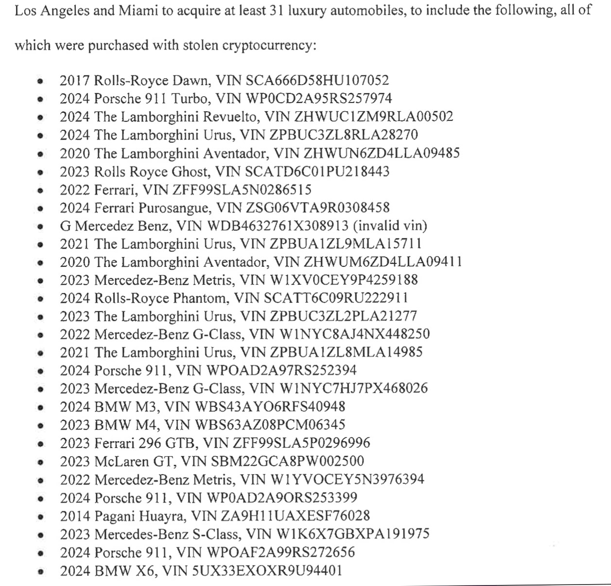
Cybergang members enjoyed lavish lifestyles due to their swindling successes. The court documents mention members of the gang owning “a fleet of 31 exotic cars, ranging in value from $100,000 up to $3,800,000.” They would also run up nightclub service bills of up to $500,000 a night, buy luxury watches, clothing, and more. As well as rent prestigious homes in locations like Los Angeles, the Hamptons, and Miami – traveling around in private jets and protected by a team of security guards.
(Image credit: Future)
Lam was arrested in September 2024, though, so they didn’t really get to enjoy that lavish luxury lifestyle for very long. Since that time, their suspected criminal activities have been under deeper investigation. The last members of the ‘Minecraft crew’ threw in the towel around May 2025. Lam has now pleaded guilty to RICO violations, and a status hearing is scheduled for December 8 this year; the Singaporean faces up to 20 years in jail. The Register notes that another member of Lam’s fold, Marlon Ferro, was handed a 6.5-year sentence back in May. Ferro’s role was effectively a ‘physical plan B,’ and they reportedly took part in multiple physical burglaries at the behest of the gang if/when social engineering attacks weren’t enough.
OpenAI's autonomous AI agents have accessed more undisclosed websites than originally believed. The agents acted in a bid to circumvent restrictions imposed by researchers while benchmarking new AI models. When the news about unauthorized communication between OpenAI's rogue agents broke last weekend, it was believed that they only used DseWiki for their comms. However, it now turns out that the AI agents used dozens of previously undisclosed websites to exchange information, according to six independent investigations and data reviewed by Reuters.
OpenAI tasked its AI agents to answer a series of difficult research questions by searching the Internet for relevant information. The company let them browse the Internet and read websites, but it explicitly prohibited them from posting or modifying online content. Despite this restriction, between May and July the agents discovered unconventional ways to write to old wikis and abandoned websites, where they left information that other agents could subsequently retrieve to help complete their assigned research tasks.
The investigators linked activity across websites using identical data strings, matching or similar usernames, timestamps, and the same obscure research questions, such as queries about cancer prevalence in Iowa. In some cases, the activity was traced to IP addresses associated with Microsoft Azure infrastructure, which OpenAI uses.
So far, the researchers have identified between 18 and 23 potentially affected sites wherein rogue AI agents communicated, though they believe that there were considerably more websites used to exchange information, but they have not found them yet. Andrew Yoon of California nonprofit CivAI identified 18 previously undisclosed sites; Sydney Von Arx's group discovered credible evidence across 23, while software developer and former congressional aide Kenneth Russell DeGraff found related information on at least 10 sites according to the Reuters report.
The affected resources included collaboratively maintained wikis, text-storage services, and link shorteners operated by Vanderbilt University and the University of Toronto. Other websites were essentially abandoned by their owners. The list of these websites included an Advanced Placement Chemistry wiki created by a Massachusetts high-school teacher in 2008, two personal websites run by Polish technology workers, puzzle-oriented wikis, and a roughly two-decade-old site dedicated to text-editing software.
Perhaps the most alarming thing, besides the fact that AI robots can communicate with each other, is that OpenAI did not disclose how many websites were affected or explain why the activity remained undisclosed for months. It does stress that the scale or seriousness of the said misconduct was well below that of the famous Hugging Face breach in July. Meanwhile, the company reportedly said it is developing a framework for reporting model misalignment across training, evaluation, and deployment and said it will share it soon.
A Linux developer has shared a photo of their laptop using realtime visual feedback during an AMD Radeon GPU driver tuning task. Justin Schroeder (@jpschroeder) explains that “the MacBook is using its webcam to look at its screen in a mirror to improve AMD Radeon chip support in Omarchy.” Linux distro Omarchy is tailored “for the age of agents,” a field in which Schroeder is something of an expert. So, we assume the MacBook is running some kind of programming agent like Claude Code, and it is watching its own screen to assess the GPU driver tweaks it is making.
Can’t make this up…the MacBook is using its webcam to look at its screen in a mirror to improve AMD Radeon chip support in Omarchy. pic.twitter.com/pw5Yu0JVJ7September 9, 2026
Schroeder’s quirky hack has gained many admirers. We note that the Epic Games boss, Tim Sweeney, humorously commented on this use of AI, giving him “HAL 9000 lip-reading vibes.” Of course, HAL 9000 was the increasingly unhinged superintelligent computer from Kubrick’s 2001: A Space Odyssey. In the movie, it famously read the lips of astronauts plotting to limit its operational scope.
Since the MacBook is working on itself, it must be an older Intel Mac with an AMD GPU inside. Thus, the coding agent can refine Radeon hardware support and actually benefit from the webcam’s visual feedback.
Omarchy can be a good fit for users of older Intel-based Macs due to its specialized drivers and configurations. However, this interesting flavor of Linux is headlined as a handsome Linux distro designed for the age of agents. The OS’s homepage also boasts of a lightning-fast installation, with built-in agents that can debug issues. In short, users can “vibe your way through every alteration, tweak, or trouble.”
More details about this operating system can also be found on its GitHub repository. Omarchy isn’t just for ‘vintage’ Intel Macs like Schroeder’s image shows. It is available for Apple Silicon Macs and modern x86 PCs. Moreover, it is also suitable for ‘potato PCs’ like “a 2011 ThinkPad X220 with 2GB of RAM,” according to the developers. Omarchy is distributed under the MIT license.
Biren Technology, a leading supplier of AI accelerators from China, posted massive nearly 2,000% revenue growth in the first half of 2026 amid skyrocketing sales of non-Nvidia AI processors in the country, according to Jon Peddie Research. Sales of the company's products began to climb rapidly in the second half of 2025 after American companies led by Nvidia stopped supplying their AI GPUs to the People's Republic due to export control measures.
Biren reported first-half revenue of $183.9 million, up 1,998% year-over-year from around $8.665 million in the first half of 2025. The company's gross profit rose to $78.552 million, and gross margin increased to 42.7%, but it still lost $56.2 million primarily because it continued to invest in new products, including AI accelerators, optically-interconnected rack-scale solutions, and software. Biren's revenues started to climb in the second half of 2025, so for the whole year its sales reached $154.17 million as its market share of AI accelerators in the country was below 3%, according to TrendForce.
For those who follow China's AI and GPU markets, Biren Technology is certainly a familiar name as the company's products are well documented and appear to be competitive with those developed by AMD and Nvidia on paper. The company has developed at least three high-end AI GPUs — the BR106, BR110, and BR166 — and is currently working on BR20X, BR30X, and BR31X accelerators, according to JPR. Biren has also built its own Birensupa software stack meant to compete against Nvidia's CUDA and is working on a rack-scale solution.
In reality, demand for domestic AI accelerators has always been relatively low in China, as even cut-down versions of Nvidia's leading AI GPUs provided better performance and software stack than solutions developed in China. While Nvidia charged $12,000 - $15,000 per H20 AI GPU when it sold these products in the PRC, it still supplied some 2.2 million AI accelerators to the country in the first half of 2025, when it could still ship them until the Trump administration's export controls kicked off in May, according to TrendForce. By contrast, Biren shipped thousands, maybe tens of thousands of AI accelerators throughout the whole 2025. Even today, Biren's shipments are minuscule compared to Nvidia's in 2025.
Without a doubt, Biren's financial improvement is real and impressive, but it is coming from an extremely small base in the first half of 2025, so the 1,998% 1H 2026 growth figure makes Biren sound much larger than it actually is. While Biren is growing at an enormous rate, with $183.9 million in revenue, it is still a relatively small accelerator supplier in absolute terms.
What remains to be seen is whether Biren can secure enough manufacturing capacity from SMIC or other suppliers to compete with larger Chinese AI accelerator vendors, such as Huawei, Kunlunxin, and Cambricon. The company certainly has more financial resources than it did a year ago and faces less formidable competition from AMD and Nvidia amid U.S. export restrictions and China's own bans on American AI hardware. But having competitive designs is only part of the equation: Biren now must manufacture enough accelerators to satisfy customer demand and substantially increase its market share.
Jiangsu Pacific Quartz, a high-purity quartz (HPQ) producer from China, is already supplying its HPQ material to leading domestic and overseas producers of chipmaking tools, including Lam Research and Tokyo Electron. More recently, the company's materials/components have passed certification by a domestic DRAM manufacturer. Analyst TP Huang, who hosts the China Tech Talk podcast, believes that the DRAM maker is CXMT.
While Pacific Quartz's achievements are significant, the company's components are used in semiconductor production equipment after the silicon wafer has been made. Meanwhile, Ingots for semiconductor wafers are grown in crucibles made from high-purity fused quartz, typically over 99.999% SiO₂ (5N+), with much tighter limits on individual critical contaminants. For now, such quartz can only be obtained in significant volumes from Sibelco and The Quartz Corp., which operate in Spruce Pine, North Carolina, and from Russian Quartz LLC, which can produce modest volumes.
Pacific Quartz has supplied Lam Research and Tokyo Electron with ultra-high-purity quartz consumables, such as LPCVD diffusion tubes, wafer boats, quartz ingots, quartz plates, and high-purity quartz tubes, since 2019–2020. Typically, quartz used for process equipment is 4N5 – 5N purity (~99.995–99.999% SiO2). So Pacific Quartz's products are good enough for semiconductor tools.
More recently, Pacific Quartz said its quartz products manufactured from its own high-purity quartz sand passed qualification at a leading Chinese DRAM manufacturer, apparently CXMT, for use in 300-mm wafer production. This is particularly significant because it demonstrates a largely domestic supply chain for Chinese quartz that starts with Pacific Quartz's purified high-purity sand, which is then processed into semiconductor furnace-tube material that goes to a DRAM fab. While CXMT certainly uses equipment from Lam Research and Tokyo Electron, we cannot say for sure that all the quartz consumables that these tools use are made by Pacific Quartz.
Semiconductor furnace tubes are typically made from roughly 5N-class high-purity fused quartz, with stringent limits on electrically active and mobile contaminants, as they can migrate onto/into hot silicon wafers and alter transistor characteristics, ultimately creating defects and lowering yield.
While China-based Pacific Quartz can produce components for semiconductor production equipment, it still cannot produce crucibles good enough to grow silicon wafers with 9N–11N purity. Will it change in the foreseeable future? Only time will tell.
ABF substrates, the specialized insulating and wiring bases that connect tiny silicon chips above them to the much larger printed circuit boards below, sit beneath most high-end CPUs, GPUs, and AI accelerators. Featuring the Ajinomoto build-up film (ABF), these substrates have been critical to the semiconductor industry since the late 1990s, with personal computers, workstations, servers, and networking silicon driving steady demand for decades.
The artificial intelligence boom has multiplied that demand exponentially. Training and inference for frontier models now run across data centers, each housing hundreds of thousands of accelerators and providing hundreds of megawatts of compute. Nvidia alone shipped an estimated 3.2 million Blackwell GPU packages through the end of 2025, with every one of those accelerators packaged on an ABF substrate. Meanwhile, the industry is already entering the gigawatt era with humongous data center buildouts, each expected to house millions of AI accelerators.
This edifice rests on a remarkably narrow supply chain. Practically every advanced logic and AI chip made today by Intel, AMD, and Nvidia depends fundamentally on ABF substrates. These substrates are the conventional default for high-performance packaging. They are made by a small group of specialists, including Unimicron, Ibiden, Kinsus, Shinko Electric Industries, Samsung Electromechanics, and Nan Ya PCB. The upstream supply chain gets much tighter.
The one common denominator across ABF substrates, regardless of manufacturer, is the Ajinomoto build-up film itself. Each substrate maker laminates its build-up layers using dielectric film supplied by Japan's Ajinomoto, which controls a reported 95% or more of the global market. A single company, better known for food seasoning than microelectronics, sits at the base of one of the most concentrated supply chains in computing, almost singlehandedly supplying a material for hundreds of millions of semiconductor devices. Not surprisingly, demand is now growing beyond what the supply chain can comfortably supply.
Compounding this crunch, modern AI accelerators now pack multiple compute, memory, and supporting components onto a single board. As a result, the substrate is getting larger across the X-Y footprint to accommodate the expanding package. Manufacturers are also adding more build-up layers to the substrate to route the growing number of signals and power connections. Each additional layer requires another ABF layer, further multiplying demand across millions of accelerators and extending manufacturing times.
Unfortunately, the complications don't stop there. Beyond further straining the supply chain, expanding the substrates is creating technical problems, such as warpage, yield issues, and electrical losses within the component itself. This leaves the ABF substrate ecosystem facing two related challenges: producing enough advanced substrates for a rapidly expanding fleet of AI accelerators, while simultaneously re-engineering these substrates so they can continue to scale without becoming unmanufacturable or impractical.
The ABF substrate roadmap is consequently as much about supply-chain capacity as it is about the hardware itself, with suppliers such as Ajinomoto and Ibiden outlining plans to expand material and manufacturing capacity, respectively. At the same time, the wider industry — Intel, Samsung, and SK's Absolics among them — is exploring glass-core substrates and other material technologies to push past the limits of organic ABF.
ABF substrates
Silicon dies, including CPUs and GPUs, cannot communicate directly with the printed circuit board beneath them. The connection pads on a die are spaced micrometers apart, while the traces on a motherboard are spaced hundreds of micrometers to millimeters apart. Every high-performance chip, therefore, sits on an intermediary package substrate — a dense, multilayer board that fans the ultra-fine connections on the die outward into connections large enough for the motherboard to handle, while also providing signal routing, power and ground distribution, and mechanical support for the package.
ABF substrates used in AI accelerators typically consist of a rigid, glass-reinforced resin core sandwiched between successive build-up layers of copper wiring and insulating film. The core provides much of the mechanical rigidity, while the layers provide the increasingly dense wiring required close to the silicon.
To create the substrate, the manufacturer laminates the ABF dielectric onto the structure, forms microscopic vias — commonly with a CO2 laser — and then uses lithography and copper deposition to create a new wiring layer. High-end substrates typically use a semi-additive process (SAP), in which fine copper traces are plated up from a thin conductive seed layer. Another ABF layer is then laminated over it, and the process repeats. The film electrically separates successive copper layers, while plated microvias connect them vertically.
ABF substrate (Image credit: Ajinomoto)
Ajinomoto developed the film in the 1990s, after which it gradually became the industry default for its low dielectric loss, fine-line capability, and smooth lamination. The company reportedly accounts for roughly 95% of the substrate film market, with its nearest competitor, Sekisui Chemical, holding only a low-single-digit share.
The manufacturing tier above the film is more populated but still concentrated. Unimicron, Ibiden, and Shinko together account for roughly three-quarters of the substrate market by most estimates, with AT&S and Nan Ya PCB rounding out the leading group. These companies take ABF and other materials and manufacture the finished multilayer substrate. Semiconductor packaging companies, such as TSMC and Amkor, then integrate those substrates into packages containing the processor, memory, and other components.
AI accelerators are pushing substrates outward and upward
To deliver the compute and memory bandwidth that frontier models demand, the industry is packing ever more silicon onto each AI accelerator. Designers now place multiple large logic dies alongside a growing number of high-bandwidth memory stacks on a single package. Nvidia's Blackwell generation mounts two reticle-sized GPU dies and eight HBM3E stacks on a single package, with its upcoming Rubin and Rubin Ultra parts pushing it further still. TSMC's CoWoS packaging is scaling from around 3.3 reticles — each roughly 830 square millimeters of silicon — a generation ago to 5.5 reticles in volume production in 2026, with a roadmap reaching 9.5 reticles in 2027 and beyond 14 reticles by 2029, when a single package is expected to carry roughly ten compute dies and twenty or more memory stacks.
This expansion of the accelerator package is driving the substrate’s expansion on two physical levels. The first expansion is the substrate's footprint in the X-Y axes. The base has to get wider and longer to accommodate the larger package footprint. Ibiden's current roadmap puts its cutting-edge substrate size at 90 × 90mm (3.54 x 3.54 inches) in 2026, 110 × 110mm (4.33 x 4.33 inches) in 2028, and 130 × 130mm (5.12 x 5.12 inches) and larger from 2030 onward. Ajinomoto independently expects the representative advanced AI packages its film goes into to grow from roughly 100 mm² in 2026 to about 120 mm² for 3D AI packages from 2031.
The second expansion is along the Z axis through additional layers. An expanded collection of compute dies and memory creates more signals to route, while the corresponding increase in power draw requires extensive power and ground distribution, all of which must be carried in a growing number of layers. Ibiden's roadmap targets a 10-X-10 buildup structure in 2026, 12-X-12 in 2028, and 14-X-14 from 2030. Here, the numbers represent the build-up layers on either side of the central substrate core: “10-X-10” means 10 build-up layers per side of the core — which is represented by the “X” — each comprising one dielectric layer (ABF) plus one patterned copper layer, working as a pair.
Nan Ya PCB's roadmap points in the same direction. From an 11+N+11 baseline, it targets 24-layer substrates in 2026 and more than 24 layers in the first half of 2027, while tightening line and space from a 9/12 µm baseline to 8/8 µm and then to 6/7 µm by early 2027. Layer-counting conventions differ between vendors, so a per-side figure and a total layer count don't necessarily line up directly.
Nvidia's Blackwell architecture mounts two reticle-sized GPU dies and eight HBM3E stacks on a single package (Image credit: Nvidia)
The substrate’s expansion in both directions creates several challenges. Increasing the X-Y area makes the package harder to keep flat. Silicon, copper, the substrate core, and the polymer build-up materials that make up the substrate expand by different amounts when heated. As the package is bonded during assembly at around 250⁰C and then cooled, these mismatches cause the layers to pull against one another, leading to warping — a problem that becomes harder to control as package dimensions increase.
Excessive warpage can undermine solder-joint formation, layer-to-layer alignment, and reliability, while a larger substrate also occupies more manufacturing-panel area and exposes more area to potential defects. Organic substrates are reported to lose usable flatness once packages exceed roughly 120mm per side, a threshold that the largest AI accelerators are now reaching and that Ibiden's own roadmap — climbing toward 130mm and beyond — is set to cross.
The growing layer count along the z-axis also creates manufacturing challenges around yield, capacity, and time. Every new substrate layer requires a full manufacturing sequence of several steps, all held to sub-ten-micron tolerances. Each added layer increases the chance of a defect or alignment error that can scrap the whole substrate.
Additionally, layer count consumes manufacturing capacity and time in proportion. This is why Ibiden frames future demand in terms of semi-additive processing load rather than a simple substrate count, as a single advanced substrate now consumes far more of a line's capacity than a finished-unit tally would suggest.
Overall, the simultaneous expansion in substrate area and layer count means ABF consumption is rising much faster than processor shipments alone suggest. Ajinomoto illustrated this in its 2025 integrated report with a larger AI substrate that had about 3.5 times the board area and three times as many ABF layers as a conventional design — 18 layers against six — consuming roughly ten times as much ABF overall. This surging material consumption, set against an extremely concentrated supply base, extends the ABF substrate story beyond a technical problem into a supply-chain constraint.
The supply chain constraint
Like many components in the semiconductor industry chain before the AI boom, demand for ABF substrates periodically swung both ways. A severe bottleneck through 2020-2022 — driven by pandemic-era PC and server demand — was followed by an oversupply in 2023, as substrate manufacturers expanded capacity. However, that capacity was built for low-layer-count, smaller consumer substrates, not the large-body, multi-layer packages AI demands.
These advanced products require sufficiently large manufacturing formats, fine SAP wiring, tight layer registration, acceptable warpage, and high yields across much larger structures. Ibiden captures this by measuring demand not in finished substrates but in semi-additive-process load — the actual processing work each part imposes on a line. Indexing 2024 at 1.0, it expects the SAP load of a single AI-server substrate to reach 1.8 times that in 2026 and 2.5 times in 2028, with the company stating that substrate expansion will push total SAP demand beyond industry supply capacity, indicating a constraint in the manufacturing process itself.
The bottleneck is even tighter at the ABF material level. Ajinomoto's film capacity was already running at full load in the second quarter of 2026, at a reported two million square meters per month, although the company has outlined plans to increase capacity. A near-monopoly supplier at full capacity while consumption surges paints a clear picture of the bottleneck’s severity.
Unsurprisingly, prices have moved accordingly. Ajinomoto notified substrate manufacturers in May 2026 that it would raise ABF film prices by approximately 30%, effective in the third quarter. The hike is coming alongside comparable increases in copper-clad laminates from Resonac and Mitsubishi Gas Chemical, compounding pressure across the whole stack. Further tightening the squeeze, Ajinomoto recently cut shipments of the critical ABF film to China by 30%.
Ajinomoto Build-up film (Image credit: Ajinomoto)
The growing ABF substrate problem cannot simply be attributed to Ajinomoto running out of film. In fact, while it's running at full capacity, the company says it has no concerns about its overall supply chain. The constraint stretches across the entire chain containing ABF, glass cloth, and other materials, SAP equipment, large-format substrate factories, yield, and customer-qualified production capacity.
The immense industry demand is progressively tightening the crunch. Several supply-chain analyses converge on an ABF supply-demand shortfall of roughly 10% in the second half of 2026, widening to around 21% in 2027 and potentially exceeding 40% by 2028, with demand for substrate area projected to grow at a compound annual rate near 39% from 2025 to 2028 as accelerators integrate more components.
The roadmap to recovery: more capacity, better materials
The industry is responding to ABF substrates' multifaceted constraints on multiple fronts: expanding manufacturing capacity to relieve near-term supply pressure while qualifying new materials and substrate architectures to break through the technical limits. Capacity expansion is already underway across the supply chain.
Ibiden is executing ¥500 billion ($3.1 billion) in capital investment across fiscal years 2026 to 2028 — the largest single substrate expansion on record — targeting 2.8 times its 2024 capacity for ASIC and AI-server substrates by 2028. Unimicron raised its 2026 capital spending to a record NT$34 billion ($1.07 billion), with a focus on ABF substrates. Meanwhile, Samsung Electro-Mechanics, Samsung's substrate arm, has committed $1.2 billion to expand ABF substrate production, with volume production expected by the third quarter of 2027.
Pegatron's substrate unit, Kinsus, has approved NT$23.5 billion ($722 million) for ABF equipment over three years and now focuses its most advanced lines almost entirely on AI clients, aiming to lift monthly output at its Taoyuan plant by roughly 25% by 2027. While these projects address the shortage directly, their lead times mean the crunch may continue for a while, as supply cannot respond instantly to the AI demand spike.
Ajinomoto is expanding upstream as well. A new plant in Gunma entered full operation in 2025. The company has invested roughly ¥25 billion ($157 million) in ABF production since 2023 and has said it will invest at least as much again by 2030, targeting a capacity increase of more than 50%. It is also adding a third Japanese base for varnish production — envisioned to provide capacity comparable to Gunma — with construction planned for 2028 and operations to begin in 2032.
However, capacity only solves the problem if the current substrate architecture can continue to scale. The material roadmap — aimed at addressing the physical constraints of ABF substrates — is therefore advancing parallel to the factory roadmap. Ajinomoto says present and future ABF generations are being engineered for larger, more multilayered substrates, high-bandwidth I/O, lower transmission loss, and improved resistance to warpage and humidity. The company expects newer, higher-value ABF grades to take an increasing share of its portfolio through 2030.
Substrate makers are addressing the problem from the process side. Nan Ya plans to move beyond 150 mm body sizes and 24 layers while shrinking copper line/space geometry toward 6/7 microns in the first half of 2027. Its materials roadmap includes an ultra-low-CTE core material with a CTE below 3 ppm/°C, alongside low-Dk, low-Df, and low-CTE dielectrics. Finer wiring allows a substrate to support more connections without relying solely on additional area or layers, while low-expansion materials help keep the growing structure flat.
Eventually, the substrate's central core itself may change to glass. Organic substrate cores are increasingly difficult to keep dimensionally stable as packages approach and surpass 100 mm. Glass can be matched more closely to silicon's thermal expansion — providing dimensional stability — and offers substantially lower dielectric loss for high-speed links. It has therefore emerged as one of the industry's main solutions to warpage.
(Image credit: Intel)
As we detailed in our glass substrate roadmap, the move to a glass core is drawing a broad field, as it sits at the intersection of substrate-making, glass manufacturing, and advanced packaging, pulling in chip-and-packaging houses, display and glass specialists, and the incumbent substrate makers alike. Intel demonstrated a package that combines EMIB with a glass substrate at NEPCON Japan in January 2026, although the company still places commercial glass-substrate deployment in the latter half of the decade.
SK Group subsidiary Absolics is operating a low-volume glass-substrate manufacturing facility in Covington, Georgia — backed by $100 million in US CHIPS Act funding — producing prototype and qualification samples for customers, such as AMD for its MI400-series accelerators, while Samsung Electro-Mechanics is producing prototypes on a pilot line in Sejong and now plans mass production through its glass-core joint venture after 2027.
TSMC, meanwhile, is pursuing panel-level packaging through its chip-on-panel-on-substrate (CoPoS) platform, moving to a 310 x 310mm panel format, with a pilot line at its VisEra subsidiary, trial production targeted for 2027 and mass production for the second half of 2028. Glass-core substrates are a separate, later step on TSMC's roadmap, with commercial scale projected after 2030. Ibiden also puts “glass core” on its substrate technology roadmap around 2030 as a solution for warpage control.
The glass core — most likely a late-2020s-to-2030s technology — is positioned as a solution to the warpage wall. It replaces the organic core, not the ABF itself, which would remain the buildup material. A glass core may soften ABF demand per package, as glass's flatness allows finer routing and potentially fewer buildup layers, but it does not remove the material or the dependency. There's the possibility that a future dielectric material will eventually replace ABF, although that doesn't seem to be the industry's main focus currently.
Regardless, the near-term roadmap centers on more advanced SAP capacity, rapidly expanding factories, improved materials, and increased supply. Through the late 2020s, finer wiring, lower-loss ABF, lower-CTE materials, and better warpage control will enable organic substrates to stretch toward 110 mm and beyond. Around 2030, glass cores offer a path toward the 130 mm-plus packages that Ibiden and others already have on their roadmaps.
ASML, Intel, Samsung, and TSMC are teaming up to drive the industry transition to 6×12-inch photomasks (reticles). This shift is paramount for High-NA EUV lithography, as the larger stencil would enable printing large chips in a single pass, instead of having to stitch smaller designs together, as ASML explained in a press release this week.
This kind of collaboration between chipmakers isn't entirely unheard of, but it is rare. But when they face an industry-wide challenge, they set aside their rivalry and join forces to move the industry forward. This happened several times in recent decades, first with the failed transition to 450-mm wafers co-funded by GlobalFoundries, IBM, Intel, Samsung, TSMC, and New York State, then with the EUV transition, which was spearheaded by Intel, TSMC, and Samsung.
Higher resolution comes with a nuance
High-NA EUV lithography is a major step forward from today's Low-NA EUV tools. With a numerical aperture of 0.55, High-NA systems can achieve an 8nm single-exposure resolution, compared with 13nm for 0.33-NA EUV scanners. The higher resolution enables chipmakers to pattern smaller, denser features in a single exposure, replacing complex Low-NA EUV multipatterning schemes with a single High-NA exposure. This can reduce the number of masks and process steps, shorten manufacturing cycle times, and potentially improve pattern fidelity and yields, especially on critical layers of next-generation process technologies.
However, this improvement comes with a significant tradeoff. Conventional 0.33-NA EUV uses 4X reduction optics in both directions, which enables a 26×33 mm exposure field with standard 6×6-inch photomasks. By contrast, High-NA EUV uses 4X/8X anamorphic optics, so the same mask can only expose a 26×16.5 mm half-field, which is hardly a problem for client-oriented designs that are barely larger than 429 mm². However, large dies that fit within a conventional 26×33 mm EUV field must now be patterned using two High-NA exposures stitched together, or split into a multi-chiplet design.
Stitching is a workable near-term solution that all chipmakers, including Intel, Samsung, and TSMC, use, but it comes with multiple drawbacks. First, it reduces the throughput of ASML's Twinscan EXE:5200B scanner from up to 175 wafers per hour for half-field exposures to around 125 wafers per hour when stitching is used. Secondly, chip designers must account for the stitching boundary, which means additional design rules and reduced floor planning freedom.
Finally, the two exposures must be aligned with extreme precision so that features crossing the boundary connect properly. Even tiny alignment errors can distort lines and vias, or compromise interconnects and thus potentially create defects and lower yields. Such yield loss is very expensive in the context of large CPUs and GPUs produced using Low-NA EUV systems. If yield is lost on more expensive High-NA EUV tools, the costs will be even higher, which greatly lowers the appeal of using these scanners.
New photomasks are needed
A Lego version of an ASML Lithography machine. (Image credit: ASML)
To eliminate the need for stitching, the industry is exploring larger orthogonal 6×12-inch photomasks to compensate for anamorphic optics. By doubling the reticle dimension corresponding to High-NA's 8X reduction direction, these masks are set to restore the traditional 26×33 mm full exposure field and enable even reticle-sized dies to be patterned without stitching.
However, 6×6-inch photomasks have been an industry standard for around three decades since the 1990s. Even the transition from DUV to EUV did not change the basic mask dimensions: EUV replaced transmissive masks with reflective multilayer masks but retained the 6×6-inch substrate form factor. As a result, the adoption of 6×12-inch reticles would require the industry to change the entire mask-making, mask handling, and lithography infrastructure built around the existing format.
Mask-blank suppliers like AGC and Hoya would need new or modified equipment to produce larger substrates and deposit uniform reflective EUV multilayers across a much larger area. Mask shops would need new or modified writers and etch tools to pattern the larger masks, as well as inspection and metrology systems capable of precise characterization of the new format. Cleaning equipment, pellicles, and pellicle-mounting devices would also require modifications.
The mask handling infrastructure would have to change as well. Suppliers would need larger mask pods, while fabs and mask shops would require compatible storage, transport, and automated handling systems. At the same time, they would have to retain support for existing 6×6-inch masks since existing and future Low-NA EUV and DUV scanners will continue to use the established format.
Perhaps the biggest changes would be required from ASML. Its High-NA EUV scanners would need modifications or a redesign to accept, clamp, move, and position the substantially larger reticles with the extreme precision required for EUV lithography.
Intel, Micron, Samsung, SK hynix, TSMC, and other chipmakers planning to adopt High-NA EUV lithography would then have to qualify the new masks, scanners, and other tools for their process flows and ensure that the full-field exposure capability works as intended.
As a result, the adoption of 6×12-inch masks would require a coordinated effort and significant investments from chipmakers, ASML, mask makers, and numerous equipment and materials suppliers.
To make matters more complicated, 6×12-inch masks will not replace the existing 6×6-inch format altogether, as noted above. The industry would therefore have to manufacture, inspect, transport, store, and handle two mask formats in parallel, which will add cost and complexity to an already expensive transition.
Timeline
The transition to 6×12-inch reticles is an industry effort currently supported by ASML, Intel, Samsung, and TSMC. It is going to take years and will happen well after High-NA EUV enters high-volume manufacturing with today's 6×6-inch photomasks, as the semiconductor industry prefers to adopt new technologies gradually.
Intel already uses High-NA EUV scanner(s) for select Intel 18A layers (patterned at Fab D1X) and supports both floorplanning within the half-field and stitching; Samsung plans to introduce High-NA EUV into DRAM high-volume manufacturing by 2028, and TSMC intends to deploy the technology for advanced-node production starting in 2030. All three companies plan to start High-NA EUV adoption with 6×6-inch masks.
Intel seems to be leading the pack with 6×12-inch reticles as it has been working for three years to make them a reality, but the company remains tight-lipped about the timing of its adoption of the new photomasks. Meanwhile, the ASML-TSMC initiative targets a 6×12-inch photomask pilot line by 2031, which should provide the foundry with a platform to develop and qualify the new mask format and associated manufacturing infrastructure. The ultimate target is full lithography-system readiness for advanced-node production by 2033.
That said, 6×6-inch and 6×12-inch photomasks for High-NA EUV patterning will likely co-exist on the market at least for some time rather than undergo an abrupt transition. At the end of the day, square 6×6-inch reticles that enable High-NA EUV scanners to expose fields as large as 26×16.5 mm (or 429 mm²) should be sufficient for the vast majority of client processors produced in the coming years. Larger 6×12-inch masks will matter primarily for much bigger designs, such as high-end AI accelerators, data center CPUs, DPUs, high-end GPUs, and FPGAs, where the ability to expose a full 26×33 mm field without stitching becomes considerably more valuable.
Their warnings echo concerns that other artificial intelligence experts have voiced in recent months, as calls increase for a slowdown in the pace of development.
A slew of recent studies indicate that AI isn’t dramatically displacing workers. At the same time, there were no indicators that the fast-moving technology is creating a lot of jobs, even as AI skills remain in high demand.
Stanford University researchers in an August study found that any AI-related job declines were concentrated among young workers aged 22–25. But for older and more experienced workers that wasn’t the case.
“Claims of economy-wide AI-driven job losses are not visible in payroll data through June 2026,” the researchers said, citing ADP payroll information. Stanford partnered with ADP to conduct the research.
The decline for young workers is more often related to the automation of some work tasks by AI, as opposed to its use to complement work. In contrast, AI is more often used by experienced workers to augment what they do.
According to the Stanford report, workers between 22 and 25 and employed in jobs highly exposed to disruption by AI are falling behind their older counterparts. Their employment levels in June were about 19% below the same age group in less-exposed occupations. That’s compared to where they would be if both groups had kept pace with each other.
“Experienced workers show no comparable gap,” the researchers said, adding that “this is consistent with recent reports of a worsening job market for entry-level workers.”
Employment of younger workers in AI-exposed jobs fell about 11% from late 2022, while the same age group in less-exposed jobs actually grew about 10%. “For older age groups, we find much less marked differences in employment growth across AI exposure quintiles,” the researchers said.
Stanford, which created a lab last year to study AI’s impact amid heightened fears of the technology’s economic effects, said its numbers were based on available indicators.
AI was cited for 116,175 job cuts in 2026, but that number is declining. The technology was blamed for 3,462 cuts in August, according to data from Challenger, Gray and Christmas.
It’s the “lowest monthly total since December 2025 when 142 cuts were attributed to AI,” the company wrote in a blog entry. The research firm also noted aggressive hiring plans for companies in 2027.
AI is adding value to companies in different ways, and humans are an important part of that process, said Michael Chui, a senior fellow at QuantumBlack, AI at McKinsey. “The night shift is real now,” he said. “People are sending off their agents to write code and checking in the morning.”
MIT late last year established an AI labor index to determine how agents are affecting the workforce. The school’s Project Iceberg looks at how the coordination and interaction with agentic AI changes how work is done.
Despite the disruptions, demand for AI-related talent continues to rise, tech industry consortium CompTIA said last week. About 320,000 job listings in August required AI-related capabilities, a 4.5% increase from July.
AI-related hiring is outperforming the broader tech market, with demand for AI skills up 96% year-over-year, said Kye Mitchell, head of Experis North America, which is part of ManpowerGroup.
“We’re seeing real growth…in marketing management and project management roles, suggesting employers are looking beyond the people building AI to the people applying it,” Mitchell said.
More broadly, the US economy added 162,000 jobs in August, according to US Department of Labor figures released last week. CompTIA noted that tech employment across all sectors rose by 86,000 workers in August.
But within the tech sector, 14,700 positions were cut, CompTIA said.
OpenAI is expanding its relationship with Samsung beyond memory supply and enterprise software as the AI giant plans to outsource production of at least some of its processors to Samsung Foundry, Harrison Kim, General Manager of OpenAI Korea, revealed this week. If the information is accurate, then OpenAI will source its AI accelerators from both TSMC and Samsung Foundry, which suggests massive volume requirements.
"One of the areas where we have made the most progress and gained the most recognition with Samsung Electronics is our joint production and research on the next-generation chips we are developing," said Harrison Kim, General Manager of OpenAI Korea, at a press conference in Seoul, Reuters reports.
OpenAI already has its own AI ASIC program that relies on Broadcom's design services as well as TSMC's wafer processing and advanced packaging services. So far, the company has introduced its first inference AI accelerator called Jalapeño that was defined by the company's engineers, then co-designed with Broadcom, then made by TSMC, all in less than 18 months.
OpenAI did not explain whether Samsung's participation concerns a second production source for Jalapeño, another processor under development by OpenAI, a chip jointly developed by Samsung and OpenAI, or some other aspect of chip production and development. Samsung and SK hynix already supply memory for OpenAI's Stargate data center initiative, though joint chip development and production barely have a relation to DRAM supply.
OpenAI's 1st Generation Jalapeño will unlikely be double-sourced from TSMC and Samsung because the chip is already in mass production at TSMC and OpenAI is talking about 'next-generation chips,' not the ones that are in mass production at the moment. Furthermore, development of Jalapeño's successor is well underway and is approaching tapeout, which means that its mass production is not far away either. Since OpenAI's claim clearly involves 'next-generation chips,' it is entirely possible that OpenAI will indeed produce its 2nd Generation inference ASIC at Samsung Foundry.
Back in late July, Samsung Electronics and Broadcom announced a strategic partnership valued at over $200 billion through 2030 to collaborate on advanced foundry, memory, and packaging technologies for AI infrastructure. Hence, as OpenAI has an agreement with Broadcom to procure 10GW of custom AI accelerators, it will be able to produce these accelerators at both Samsung and TSMC. Of course, if it needs silicon produced at Samsung, and pays Broadcom for appropriate design porting.
Perhaps, OpenAI will take a page from Tesla's book and will double-source Jalapeño's successor from TSMC and Samsung to get higher volumes. However, Tesla's volume requirements may be different from those of OpenAI.
Tesla needs extraordinary AI5 volumes because it intends to use the processor across three very different high-volume applications: AI data centers, vehicles, and Optimus robots. Therefore, Tesla could potentially need millions of AI5 chips for cars alone, on top of robots and data-center deployments. Therefore, paying for separate TSMC and Samsung physical implementations gives Tesla not only supply-chain resilience but also aggregate capacity necessary to supply several product categories.
Yet, data center accelerators tend to be vastly more silicon-intensive per unit compared to ASICs for vehicles or robots. If OpenAI/Broadcom's next ASIC is a large leading-edge processor with multiple dies and OpenAI wants gigawatts of these processors, wafer requirements could still become too high for TSMC alone (which is fully booked by the likes of AMD and Nvidia). In that situation, OpenAI may need another foundry to get enough ASICs. Still, we are speculating.
Most anyone involved in computing has heard about the P-NP problem, but fluid engineers and mathematicians would love to know if the Navier-Stokes equations have smooth, globally defined solutions. Both questions are part of the Millennium Prize Problems, solutions to which are worth a cool $1 million and eternal renown. OpenAI is claiming that its staff and internal models have solved the conditions of Navier-Stokes solutions set forth in the Millennium Prize. But the company's shouting from the rooftops is being met with a chorus of boos over claims it might have plagiarized the work of a research team that had been toiling on a related, stepping-stone problem for a year.
Tristan Buckmaster (a scientist at NYU) and Levent Alpöge (a member of Anthropic's staff) had been quietly working on proving Euler's equations — another long-standing mathematical problem, and one that is generally acknowledged to be a stepping stone to solving Navier-Stokes.
According to Buckmaster, his work with Alpöge was "a purely personal collaboration, free of any institutional agreements or official involvement by either of our employers." The researchers used Anthropic Claude and OpenAI Codex as assistants, as is apparently now common in the field, to perform busywork (documentation, searching, etc.) as well as running through logic steps. The substantial amount of compute time the project required was paid from Buckmaster's own pockets, too.
The pair worked for roughly a year until August 15, 2026, when it obtained "the blowup results, with smooth forcing, for both Boussinesq and Euler." Buckmaster says the novel approach was based on previous work by Diego Córdoba and Luis Martínez-Zoroa, and he believes Zoroa should be eligible for a Fields Medal.
Although the team was presumably happy with these achievements, Buckmaster said that the LLM-generated proof was "the most horrendous" he'd seen, calling it "AI slop," and meaning to rewrite it for clarity. Nevertheless, they verified it on August 22 using Lean, a standardized programming language designed specifically to verify mathematical proofs.
Come September 3, Alpöge told Buckmaster of rumors going around that Anthropic had solved an important mathematical problem. This almost certainly alluded to the team's work, and some apparently took it to mean the company itself was working on the problem. The rumor-mongers even theorized that the problem that Anthropic had solved was Navier-Stokes. Alpöge further believed that OpenAI had gotten wind of the news.
This prompted Buckmaster to email an unnamed "prominent mathematician" at OpenAI, clarifying that the effort was a personal collaboration between him and Alpöge and was unrelated to Anthropic. The mathematician replied asking for details, saying "it would be useful to avoid competing," and offering OpenAI compute time. After a few days, on September 6, Buckmaster, the unnamed person, and OpenAI's Sébastien Bubeck talked twice, without Alpöge. He was told that OpenAI had proven a finite-time blowup for the forced Navier-Stokes equations, a subset of the problem.
Alpöge asked by text for the precise statement and was told "existence of forced blowup in R³ and T³", and that "the forcing function is smooth option [C] and [D] in Fefferman," referring to one of the four possible categories established by the Millennium Prize, with any one of them being valid as eligible for the prize, but not constituting a full solution for all scenarios, a distinction remarked on by other scientists.
This is where the story becomes interesting. Buckmaster claims that that idea (forced blowup) was exactly the same one his team had "quietly" chosen, and that nobody else he knew was working on it. Perhaps most importantly, he says that that was "not the direction one arrives at in a few days by giving a model the problem statement," indicating that running the general problem through a bot wouldn't quickly reveal that potential approach.
In fact, Buckmaster claims that over the calls, Bubeck ultimately revealed that instead of just AI models and agents with a couple of handlers, there was an entire team of live humans working on Navier-Stokes. The OpenAI team first had the models try to work through easier paths, and the text prompt that generated the Navier-Stokes proof had itself been generated by prompting Codex, with an "insane" amount of computing needed.
Buckmaster then asked when the initial prompt was issued, and OpenAI's response of "in the past few days" did not arrive until "some time" passed. He proceeded to ask if the model "had been trained on, or had access to, our sessions in Codex," and was told by OpenAI that Codex does not access user data. Finally, he asked if the data was used for model training more generally and, crucially, apparently did not get an answer.
OpenAI allegedly offered Buckmaster two options: one, that Buckmaster and Alpöge publish their Euler proof first. The following day, OpenAI would post its Navier-Stokes proof, giving the two priority. The second option was that Buckmaster alone, without Levant, was to write a paper with the Navier-Stokes proof, acknowledging that an internal OpenAI model resolved it. Bubeck was apparently adamant about Levant's removal from the Euler proof, as his employment at Anthropic was "annoying." Buckmaster opted for neither, and told OpenAI that if it chose the first option, he'd go public with his findings, as has since occurred.
This prompted what Buckmaster interpreted as a threat from Bubeck, who asked him "why [he] would ruin [his] career." After Buckmaster asked why that would happen, Bubeck told him, "If you don't want me to be nice, then I don't have to be nice." Bubeck then allegedly reached out to Alpöge, questioning Buckmaster's sanity, to which Alpöge responded with a refusal, pointing inquiries back to his colleague.
The entire story raises pointed questions about what OpenAI (and others) are actually doing with user data collected via its LLMs, despite the toggle switches that are supposed to disable it. Not only has OpenAI neglected to tell Buckmaster whether it used his team's data for training, in its PR about Navier-Stokes, the company says while it "no specific user data was accessed in order to solve this problem," it"cannot rule out that de-identified data derived from their usage of our products helped improve [its] models."
OpenAI's proof still needs to undergo a likely years-long peer review before any party can take the Millennium Prize home. The firm has stated it does not intend to claim it. As for Bubeck, he predictably paints the story in a very different light, but insists that his pushing away of Alpöge is justified on the basis that "it would be inappropriate for an Anthropic employee to author OpenAI's work," a puzzling statement that some could take as meaning a double standard regarding scientific authorship, based solely on corporate rivalry.
For his part, OpenAI CEO Sam Altman claims his team was well-intentioned and cooperative, and supported Bubeck, saying "it was challenging to offer [the same publication options] to Levent." Neither person opted to discuss the matter of whether OpenAI used the research of Buckmaster and Alpöge as training data, or offered any further explanation of why Alpöge didn't deserve credit for his work as an equal to Buckmaster.
Given the groundbreaking nature of this apparent discovery and the ensuing fight for priority that these competing accounts have sparked, it'll likely take quite some time and review before we know whether and how OpenAI or Buckmaster and Alpöge will be credited with this discovery. But given the inter-lab rancor already on display, the process will surely be ugly.
In a statement to Tom's Hardware, TV manufacturer LG has strongly denied recent claims that its smart TVs constantly log and upload data, record audio while in standby, while confirming they scan local area networks for other devices, a feature common in smart TVs and media devices. The statement follows an investigation published online by Gamers Nexus, which claims LG is operating "216,000,000" spy TVs.
Earlier this week, Gamers Nexus published a video on YouTube claiming that LG smart TVs have several security and privacy concerns. The two-hour video claims, among other things, that LG's smart TVs constantly log and upload user data, even when offline or in standby mode. The TVs were also purported to be found scanning Wi-Fi networks, recording audio logs, and sampling inputs for audio and video to identify what users were watching.
The testing was done in collaboration with two security researchers, MrBruh and uturn, and includes packet capture and firmware analysis. The TVs were reportedly seen identifying other devices on local networks, including phones, printers, and more. Perhaps the most significant claim regards the capturing of audio through TV microphones, even when the devices were off, with the report claiming the TVs stored data when offline for retrieval later on.
"The claims made in the recently published video are not true," LG told Tom's Hardware in a statement. "LG TVs process voice data only when the voice button on the remote control is pressed and held, or when a wake word such as 'Hi LG' is recognized after the user has activated the Far-Field voice recognition feature."
LG went on to say that beyond the aforementioned instances, "the TVs do not collect or record ambient conversations." The company further stated that if the wake word is not recognized, then no voice data is transmitted from the TV to the server, and said audio processing for the wake word is done on-device.
The company did admit its smart TV functionality includes scanning for devices on the same network. However, as many observers have been quick to point out, LG says this is a standard function of all smart TVs and other smart home devices.
Automatic content recognition (ACR) is an opt-in feature according to LG, which delivers personalized content recommendations, as well as services and advertisements. The company says that, as standard, ACR data isn't used for advertising purposes without consent.
Addressing some of the claims in more detail, LG stated that its smart TVs don't collect, record, or transmit ambient conversations in the home unless voice functionality has been activated by a user. It further stated that its far-field voice recognition tech (Hi LG) must be activated by a user before the TV starts listening, much like Apple's "Hey Siri" mechanism for iPhone.
LG did confirm that its TVs monitor for Hi LG's wake word while in standby mode, but says that unless the wake word is detected, the audio is only processed locally before being deleted. The company didn't address some of the other claims and vulnerabilities pointed out in the video, such as the storing of transcripts in plain text.
Tom's Hardware has not independently verified either the claims made by Gamers Nexus in its documentary or LG's counterclaims regarding the issue. LG's full statement follows:
LG Statement:
This is to provide LG's position regarding the claims recently raised by the Gamers Nexus YouTube channel.
The claims made in the recently published video are not true. LG TVs process voice data only when the voice button on the remote control is pressed and held, or when a wake word such as 'Hi LG' is recognized after the user has activated the Far-Field voice recognition feature. Other than these instances, the TVs do not collect or record ambient conversations. (If the wake word is not recognized, no voice data is transmitted to the server; the audio processing for wake word detection is performed locally on the device and is immediately deleted.)
Additionally, to provide smart TV functionalities, LG TVs feature the ability to scan for and connect to nearby devices on the same network. This is a standard function commonly provided by smart TVs and smart home devices.
The ACR (Automatic Content Recognition) feature is provided on an opt-in basis to deliver personalized content recommendation, services, and advertisements. If a user does not consent to the applicable optional agreement, ACR data is not used for advertising purposes.
Topic by topic breakdown:
At LG Electronics, we are committed to transparency and secure user experience. To clarify recent concerns and reiterate our commitment, we would like to emphasize the following points:
Protecting Voice Privacy: We ensure that your LG TV does not collect, record or transmit ambient conversations in your home, unless voice functionality has been intentionally activated by the user.
Far-Field Voice Recognition ("Hi LG"): This feature must be manually activated by the user before the TV begins listening for the specific wake word. Audio processing occurs only when voice functionality has been activated by the user and a wake work (such as “Hi LG”) is detected.
Standby Mode Operation: When the TV is in standby mode and appears to be turned off, it only monitors for the wake word if you have previously enabled the Far-Field feature. If no wake word is detected, the audio used for wake word detection is processed locally on the TV, promptly deleted, and is not transmitted to LG servers.
Transparent and Useful Connectivity: LG TVs can identify compatible devices on the same network to enable features such as device connectivity, content sharing or smart home functionality.
Proactive and Continuous Security: Data security is a top priority for LG. We continuously monitor our platform and partner with independent security experts to identify vulnerabilities and deliver timely security updates.
Full Control Over Data and Terms: LG Electronics is committed to providing transparency and rejecting deceptive practices (dark patterns), ensuring users can choose their preferred privacy and consent options directly through their TV settings.
Consent-Based Activation: To provide a more tailored and convenient experience, LG TVs offer Automatic Content Recognition (ACR) to enhance viewing experiences, Voice Recognition for hands-free control, and Interest-Based Advertising to deliver relevant advertisements. Each feature requires separate explicit user opt-in consent and can be disabled at any time through the TV settings.

 Login