
❌

Normal view

The Bayeux Tapestry: how optical techniques have let this artwork come home
30 July 2026 at 10:00
The Bayeux Tapestry
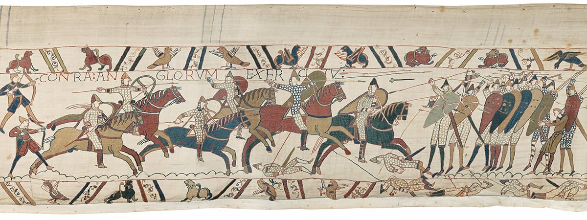
History in the making The Bayeux Tapestry is on display at the British Museum in London until July 2027 but you can view it for free online thanks to advanced optical imaging techniques. (Courtesy: © La Fabrique de patrimoines en Normandie, Antoine Cazin)

A few years ago, I was lucky enough to see the Bayeux Tapestry – the famous embroidered cloth depicting the Norman invasion of England in 1066. More than 900 years old, this historic piece of art is only 50 cm wide but more than 68 m long. It’s also extremely fragile, which why I was astonished when I heard that the Bayeux Tapestry was going to leave its home in Normandy and be transported across the English Channel to the UK.

The loan of the artwork, which was agreed between former British prime minister Keir Starmer and French president Emmanuel Macron last year, has now taken place. The tapestry arrived under police escort on 10 July and will be on display at the British Museum in London from September 2026 until July 2027. It is the first time the tapestry has been back in England, the country where this linen cloth was originally made.

I’m fascinated by how non-invasive optical techniques have been crucial in advancing our understanding of the tapestry

So what’s all this got to with physics? Well, I’m fascinated by how physics – and specifically, non-invasive optical techniques – have been crucial in advancing our understanding of the tapestry and its historical significance. Thanks to physics-based equipment developed by hi-tech manufacturers, we’ve learned about how the Bayeux Tapestry was initially made, what damage it subsequently suffered, how it was repaired, and the nature of its current condition.

Such information is vital not only for increasing our historical awareness, but also for current conservators who want to understand the tapestry’s underlying condition and find out how to preserve it for future generations. And before the pedants write in, yes I know that while it’s known as the Bayeux Tapestry, technically it’s an embroidery. That means it was created by stitching woollen threads onto a linen backing, which is helpful to know when reviewing the physics involved.

Optical sleuthing

The beauty of using optical methods to study the Bayeux Tapestry is that they are non-destructive and non-intrusive – and so can typically be applied in situ. In 2017 a three-year project was started, in which conservationists used high-resolution 2D imaging, photogrammetry, multimodal scanning and advanced image reconstruction techniques to determine the tapestry’s condition and conservation needs. The project revealed considerable information about how this artwork was created and modified over time.

Thanks to these high-resolution images, we now have a single digital map of the entire tapestry, making it possible to zoom in and look at individual threads. It’s yielded information such as the width of stitches and the positions where the wool threads cross the original linen background. As a result, historians now believe the tapestry was made by a single group of embroiderers, who – knowing the skills that existed at the time – were probably based in Canterbury, UK.

Techniques such as infrared spectroscopy and fluorescent and reflection ultraviolet imaging have revealed information about what’s underneath the surface of the tapestry

From the size and direction of the stitches, we also think the outlines of the figures were stitched first, with the shapes filled in afterwards using coloured wools in a strict, specific order. Meanwhile, techniques such as infrared spectroscopy and fluorescent and reflection ultraviolet imaging have revealed information about what’s underneath the surface of the tapestry. In particular, they’ve located the presence of stains such as glue, wax (dripped from candles that lit the tapestry) and even oil from the hands of people who touched it.

Infrared light passing through the dark-coloured wools have also revealed original sketch lines that were drawn on the linen base before the wool stitching started. It reveals the original artist’s draft, likely to be someone familiar with manuscript drawing – perhaps an illuminator of religious books.
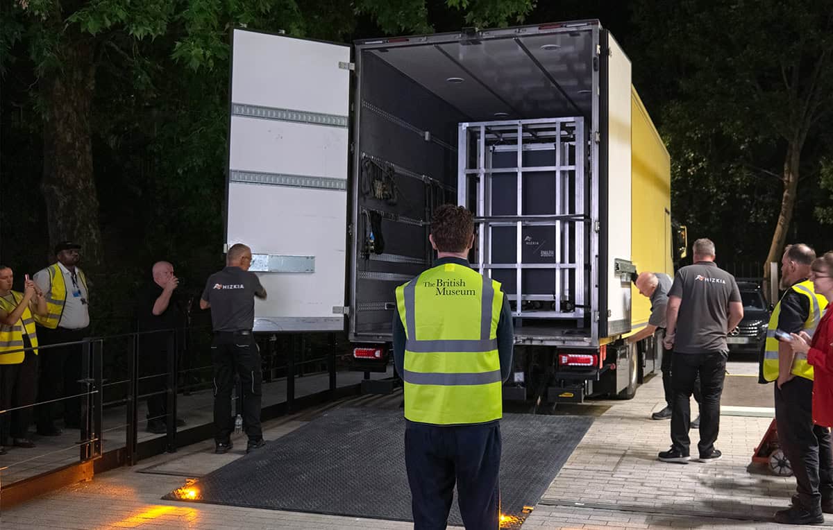
The Bayeux Tapestry arriving in London via lorry
Successful trip The Bayeux Tapestry was transported from Normandy to London in a climate-controlled crate – the journey having been sanctioned only because conservationists had pain-stakingly imaged, protected and studied the embroidered cloth. (Courtesy: © Trustees of the British Museum)

3D imaging with photogrammetry

Researchers in France, led by Stéphane Le Mouélic from Nantes University, who originally did a PhD in astrophysics, have also used computer software to combine more than 440 overlapping 2D photos taken from multiple angles to create a detailed 3D model of the Bayeux Tapestry (J. Cult. Heritage 71 211).

It digitally “irons out” all the sags and wrinkles in the line fabric, recreating the original, “flat” tapestry and allowing the original physical shape of the artwork to be revealed for the first time. The 3D model can be viewed for free at the Bayeux Museum website, allowing historians, researchers and members of the public to study it without having to handle the delicate material.

Physics-based techniques have also allowed us to deal with the fact that parts of the fabric have been repaired over the last 900 plus years. Some of those repairs used non-authentic dyes and colours, while others covered up the original stitching. But using computer vision and image processing, threads that were added later can be subtracted digitally, providing a clearer, corrected view of what the original tapestry looked like.

Finally, optical tools can help keep the tapestry safe for future generations. Museum curators need to know if the cloth is sagging, tearing, or changing shape over time. Instead of putting heavy tools on the cloth, lasers can scan the cloth to accurately map of the contours of its surface. By repeating this exercise every few years, conservationists can spot if any part of the cloth has stretched or sagged, enabling minor problems to be rectified before they end up causing significant damage.

Without the huge amount of investigative and restorative work carried out, the Bayeux Tapestry would never have been allowed to make the journey to London

In 2025 Le Monde newspaper reported that experts had, over the previous five years, meticulously documented 24,204 stains, 9646 holes and 30 tears in the artwork. Without the huge amount of investigative and restorative work carried out, the Bayeux Tapestry would never have been allowed to make this year’s journey to London. Advanced and detailed optical measurement has “de-risked” the tapestry’s trip.

Tickets to the British Museum exhibition are reportedly being snapped up faster than those for Glastonbury. So if you don’t get to see the tapestry in person, feel free to marvel at this wonderful historical artwork by checking out the interactive online digital copy. It really is physics and history in the making.

The post The Bayeux Tapestry: how optical techniques have let this artwork come home appeared first on Physics World.
‘Photonic multi-lane highway’ enjoys insulator-free topological protection

28 July 2026 at 09:20

A new type of “photonic multi-lane highway” that can carry multiple topologically-protected optical signals at once – without the need for a bulky insulator  – has been demonstrated by researchers in China. The technology, which relies on a new type of material called a photonic valley half-semimetal to achieve topological protection, is currently at the prototype stage. However, the researchers believe that, if fabrication challenges can be addressed, the combination of spatial efficiency and topological robustness could be promising for future photonic technologies.

In the past 20 years, photonic topological insulators have become widespread for connections in devices such as on-chip photonic circuits because their edge modes can only conduct light in one direction and are therefore are inherently immune from scattering off imperfections. However, the protected edge mode of a topological insulator comes at a cost: the bulk must have an optical band gap, which means it must be opaque to the relevant frequency. Meanwhile, the photonic analogue of another concept from electronics has also become popular in optical waveguides. Gapless photonic semimetals – analogous to graphene –  can be placed between topologically distinct optical insulators to broaden the guided modes, but non-guiding insulating claddings are still required.

To address the fundamental trade-off between spatial efficiency and topological protection in conventional topological waveguides, researchers in the group of Che Ting Chan at the Hong Kong University of Science and Technology in China and their collaborators introduced a novel photonic structure called a photonic valley half-semimetal. Here, the valley degree of freedom refers to inequivalent local energy extrema in momentum space, which can be used as independent degrees of freedom for transport. Crucially, a single photonic valley half-semimetal plays a dual role via its two valley channels: one valley acts as a gapless semimetal that enables waveguiding, while the other functions as a topological insulator that provides a topological barrier for the corresponding valley mode in adjacent regions.

Four stacked layers

The researchers designed a waveguide comprising four stacked layers of a honeycomb structure made from interconnected rods of the magnetic material yttrium iron garnet, which interfered with the propagating photons. By altering the diameters of the rods or the magnetic field, the researchers  constructed four inequivalent photonic valley half-semimetal domains and arranged them in a specific periodic sequence. This creates adjacent domains that mutually insulate each other.

Xiaohan Cui is lead author on a paper in Nature that describes the research. She explains that the underlying topological physics is similar to that in a traditional photonic topological insulator.

“The important difference lies in how the mode is spatially implemented,” she says, “In a conventional photonic topological-insulator waveguide, two gapped bulk domains meet at an interface, and the propagating mode is tightly localized to that interface. Most of the surrounding insulating material remains inert, serving only as cladding.”

In the present configuration, however, the researchers were able to use the blocked valley as topological protection for unidirectional propagation in the neighbouring domain, and utilize this to create a four-lane highway, with two lanes in each direction, that could guide signals around sharp bends and through constrictions without backscattering or inter-lane crosstalk:

No wasted space

“The architecture transforms the usual narrow interface state into a set of directly adjacent, large-area waveguiding lanes. Consequently, no region of the device is ‘wasted’ as inert cladding,” explains Cui.

The team’s current device works for microwave radiation but the team says that the design could be adapted and extended to operate at higher frequencies.

“The present experiment is a proof of principle demonstration at microwave frequencies, so one clear next step is to move the concept towards higher-frequency, chip-scale integrated photonics platforms, thereby paving the way toward ultra-compact topological photonic circuitry,” says Cui.

The researchers believe application in the terahertz regime should be possible using magnetized semiconductors such as indium antimonide. However, non-reciprocal applications at higher frequencies could be challenging owing to the weakness of magnetic effects.

“The major experimental challenges will be to realize these higher-frequency designs while managing geometric complexity, fabrication tolerances, and propagation loss, and ensuring efficient coupling with practical sources, detectors and other photonic components,” she explains.

Quantum optician Mahmoud Jalali Mehrabad of Massachusetts Institute of Technology believes the work brings an important issue into focus. “A paper doesn’t always have to have the perfect solution as long as it highlights and really streamlines a key problem…To me this paper does that,” he says. “Spatial efficiency has been a problem in topological physics and the question is why? Is there any other way to destroy this trade-off? It shouldn’t be a side problem in the supplementary material of a paper – this is a big problem.” Whether or not the researchers can make their own solution viable, he says, “time will tell”.

The post ‘Photonic multi-lane highway’ enjoys insulator-free topological protection appeared first on Physics World.

From ideas to industry: a theoretical physicist’s journey into Silicon Valley

1 July 2026 at 11:00

When Ryan Hamerly was a 15-year-old at Boulder High School in Colorado, he spent his summer building a Tesla coil after seeing a classroom demonstration. “I thought that was really, really cool,” he recalls. “I wanted to make one myself, and as a result I ended up studying the theory of electricity and magnetism over one summer.”

In hindsight, Hamerly realizes he didn’t use much theory to construct the coil, which became part of a school physics project. “Most of the design was based on things I had read on the Internet,” he explains, “but I did try to teach myself electricity and magnetism – and it did work in the end.”

In 2006 Hamerly’s interest in physics took him to the California Institute of Technology (Caltech) for his undergraduate studies. Keen to do graduate research, Hamerly was most fascinated by fundamental theoretical problems in quantum field theory, such as dark matter and quantum gravity. But as he started toying between different options, he had a chance encounter with Hideo Mabuchi, an applied physicist at Stanford University.

“One thing that Hideo told me that I thought was particularly fascinating,” says Hamerly, “is that quantum field theory is just a generic tool that applies in many other fields.” He therefore ended up doing a PhD in optical and quantum computing under Mabuchi’s supervision, which he completed in 2016.

Hamerly then moved to Japan, where he studied at the National Institute of Informatics in Tokyo – a time he characterizes as “sort of a postdoc, but more an excuse to travel for a year”. He did, though, get a paper out of it “so it wasn’t wasted”. In Tokyo, Hamerly worked with Mabuchi’s longtime friend Yoshihisa Yamamoto – a quantum optics researcher who had previously led a group at Japanese telecoms giant NTT for over two decades.

Step into industry

When Hamerly returned to the US in 2017, he did a formal postdoc under quantum photonics engineer Dirk Englund at the Massachusetts Institute of Technology (MIT). And in a fortuitous turn of events, Yamamoto also came to the US to establish the Silicon Valley start-up NTT Research, with the intention of forming collaborations with US universities.

“[Yamamoto] just called me up and said they had a position at NTT to work in optical computing,” he says. “At the time it made most sense to stay at MIT working as a collaborator [rather than relocate to the NTT campus] because that was where a lot of our experiments were being done.”

Today, Hamerly is a senior research scientist at NTT Research’s Physics and Informatics (PHI) Lab in Sunnyvale, California. He divides his time between MIT – where his collaboration with Englund continues – and the PHI laboratory, about 15 km from Stanford. He works at the intersection of optics, deep learning and quantum computation. For example, one of Hamerly’s projects looks into ways to reduce the energy consumption of AI data centres using optical interconnects in place of electronic ones.

Researchers hope it might one day be possible to design processors that perform calculations using optical logic that are either impossible, or at least energetically unfeasible, using electronic logic. To this end, in January 2026 Hamerly co-founded Opticore – a company producing photonic integrated circuits for energy-efficient, high-speed AI – with UC Berkeley professors Mengjie Yu and Zaijun Chen, who was previously a postdoc in Englund’s MIT group.

Different setting, same science

Hamerly does not view his place at NTT Research as purely an industry position. “The mission at NTT Research is about generating ideas that will ultimately have some use in industry,” he explains, “but the fundamental focus is on those ideas and on the research.”

The mission at NTT Research is about generating ideas that will ultimately have some use in industry

His experience at NTT Research has shown him that an industrial lab can be smaller and more focused than one at a university – but that can be a double-edged sword. “[At a university] it’s nice to be able to go into seminar rooms and see a talk from a travelling world expert in a different field,” he says, “but on the other hand, the average person [at NTT] tends to be a lot more experienced and productive than say a graduate student in academia who is still learning.”

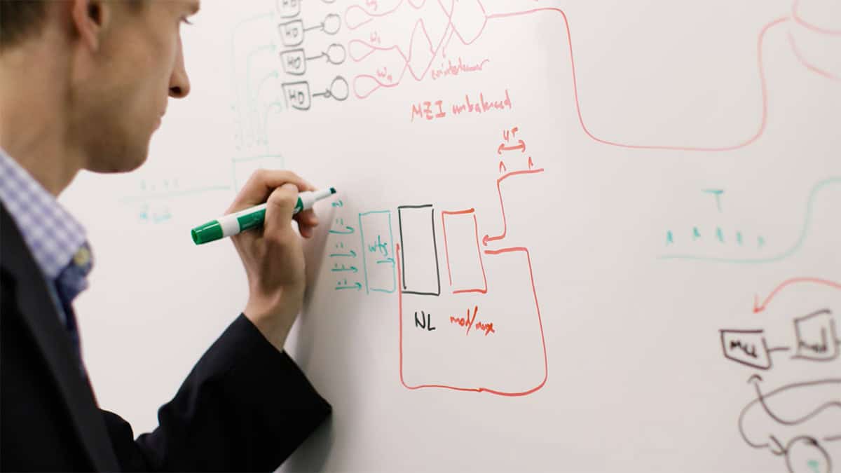
Ryan Hamerly writing on a whiteboard
Starting out Ryan Hamerly recently helped launch photonic processor start-up Opticore alongside his academic collaborators. (Courtesy: NTT Research, Inc)

However, the chance to meet and interact with scientists from different areas is still the same. “Science is science, regardless of what institution you’re affiliated with,” he says. “We’re still doing the same things: we do research in a lab, we write up the results, submit them and publish them in journals, and we go to conferences and present our work.”

Hamerly still sees himself as principally a theorist. He spends much of his time writing computer code – occasionally for models that run on a supercomputer but usually for models that can run on his laptop. The rest of his time is focused on writing papers, travelling to present work, responding to reviews or in meetings.

Looking to the future, Hamerly believes that technology will impact research, but that the core elements of a researcher’s role are likely to remain similar for the foreseeable future. “The job of a researcher before the Internet, for example, is not too different from a post-Internet researcher,” he says, pointing to how you still have to communicate research via papers and conferences, and understand the field by reading others’ publications.

“There will definitely be changes in the way you do every one of these things in the next 10 years, especially with AI, but I don’t see any of them becoming optional.”

For young researchers entering the field, Hamerly advises keeping your options open. He did not envisage himself leaving full-time academia and work in an industrial lab, but switched because it offered a better opportunity to pursue the research he wanted to do. “They are both good routes to do research,” he concludes, “but you might find – based on which offers you get – that one is better than another.”

The post From ideas to industry: a theoretical physicist’s journey into Silicon Valley appeared first on Physics World.

❌