❌

Normal view

Exciton wavefunctions come into view

1 October 2026 at 09:00

Physicists have experimentally reconstructed the quantum probability distribution of an exciton for the first time using super-fast spectroscopy. By simultaneously capturing the spatial and momentum spreads of these short-lived quasiparticles, the work adds to our understanding of how excitons evolve in complex materials. According to members of the research team, this improved understanding could lead to advances in organic photovoltaic devices.

When light shines on materials such as insulators and semiconductors, the energy from these incident photons can sometimes promote electrons in the material to higher energy bands, leaving behind positively charged holes. The electron and hole can then bind together, forming a neutral excited quasiparticle known as an exciton.

Excitons play a key role in light harvesting in optoelectronics devices, but their quantum mechanical structure has proved notoriously difficult to study. Among other reasons, this is because the excited electrons decay back to their original states within just picoseconds (10-12 s), and standard spectroscopic techniques are not fast enough to simultaneously probe the spatial dimensions of the quasiparticles’ orbits and their momentum profiles within that time limit.

Photoemission orbital tomography

In the new work, physicists led by Peter Puschnig of the University of Graz, Austria, together with colleagues at Marburg University and Forschungszentrum Jülich in Germany, got around this problem thanks to a technique called time-resolved photoemission orbital tomography (trPOT). This technique combines pump-probe photoemission spectroscopy with momentum microscopy and offers resolution at the femtosecond (fs, 10-15 s) scale, making it well-suited to capturing the exciton wavefunction.

Puschnig and colleagues began by applying an ultrashort normal-incidence laser pulse with an energy of 2.35 eV to an organic semiconductor called alpha-sexithiophene, which is employed in optoelectronic applications such as solar cells. This pulse generated the excitons. The next step was to eject the electrons from these excitons using a second, linearly polarized laser pulse with a relatively high energy of 21.7 eV. This process is known as photoemission.

“If we then measure the energy and direction of the ejected electrons, theoretical models allow us to infer their quantum-mechanical state,” Puschnig explains. “And by varying the time between the first and second laser pulses, we are able to obtain snapshots of the exciton at different times after its creation.”

The team found that the exciton in the sexithiophene films initially extends over a distance of approximately 1.5 nm, or roughly three molecules. Within 400 fs of its creation, though, its size contracts by about 25%. “What makes this particularly exciting is that we are not just measuring an energy or lifetime but are also gaining access to the quantum-mechanical wave function of the exciton itself, including its spatial structure and phase,” Puschnig says.

Coordinating demanding experiments and theory

Puschnig says the idea for the experiment grew out of the team’s earlier work on photoemission orbital tomography (POT), including a 2021 proof-of-principle study showing that it could be extended into the ultrafast regime. “The main challenge was coordinating demanding experiments and theory: producing well-defined molecular films; transporting them under ultra-high vacuum from Jülich to Marburg in a vacuum suitcase; performing ultrafast photoemission measurements; and carrying out computationally intensive ab-initio calculations in Graz to interpret the data,” he adds.

The work, which is detailed in Physical Review X, provides a new way to study excitons directly in real space and follow their quantum-mechanical evolution in time. According to the researchers, it could help us understand how excited states evolve into charge-separated states in the donor/acceptor systems that occur in organic photovoltaics, where the electron and hole can begin to separate after photoexcitation.

The researchers say their next goal is to move from the relatively simple exciton they studied to more complex systems. “We want to observe how charge-separation processes are controlled by the molecular and electronic structure of a material,” Puschnig tells Physics World. “Doing this will be particularly interesting because charge separation is the crucial step between absorbing a photon and generating a usable electrical current in an organic solar cell.”

The post Exciton wavefunctions come into view appeared first on Physics World.
Upconverting colloidal quantum dots bring ‘colour vision’ to the infrared

20 August 2026 at 12:06
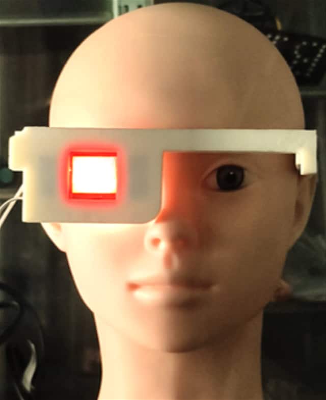
Infrared visualization Wearable eyeglasses. (Courtesy: Fu et al., Sci. Adv. 12, eaed0245 (2026))

Most people can perceive different colours in the visible range of the electromagnetic spectrum – at wavelengths between about 400 and 700 nm. However, our eyes cannot see infrared radiation, let alone perceive infrared “colours”. But now a team at China’s Beijing Institute of Technology has created colloidal quantum dot-based light upconverters that convert the infrared to the visible while preserving the spectral notion of colour. These nanostructures can be incorporated into wearable eyeglasses and, more ambitiously, could someday be implanted directly into the retina.

Photoreceptors in mammalian eyes contain light-absorbing pigments consisting of opsins and their covalently linked retinals. Infrared light at wavelengths greater than 700 nm cannot be absorbed by these photoreceptors, so when such light reaches the retina no corresponding electric signal is sent to the brain. Seeing infrared radiation could reveal otherwise invisible features and improve night vision, which relies on infrared light.

In recent years, researchers have made great strides in developing materials that capture photons with lower energies (in the infrared, for example) and re-emit them as photons with higher energies (typically visible or ultraviolet light). This process is known as upconversion, and the emitted light is said to be anti-Stokes shifted. This has led to the development of photoreceptor-binding upconversion nanoparticles that convert infrared light into visible emissions. These have been injected into mouse eyes and have been used to create wearable lenses for humans – with nonlinear upconversion projecting infrared-transformed visible light onto the cornea. While effective, these applications are limited to the narrow near-infrared (NIR) spectral range.

Confined electrons

Now, a team led by Ge Mu and Xin Tang studied a structure made up of semiconducting mercury telluride (HgTe) colloidal quantum dots (CQDs) atop an organic light-emitting diode (OLED). The OLED contains two light-emitting layers, one red-light-emitting and one cyan-light-emitting. Because of the small size of the CQDs, the electrons in them are confined in all three directions. This means that the electrons are restricted to discrete and separate atomic-like energy subbands rather than having access to a continuous band of allowed energies as they would in a bulk material.

When the CQDs absorb photons with infrared wavelengths, spanning the NIR to short-wave infrared regions, they produce excited carriers (electrons and holes) that then travel from their different energy levels into the OLED. This is a seamless process because the OLED is designed so that its electronic bands align with the sub-bands of the HgTe. When either the light intensity or the wavelength of the incident infrared light changes, explains Tang, the excited photocarriers are transported and recombined in the different emissive layers of the OLED thanks to the hole-trapping barriers that were engineered in these layers. The result is infrared-to-visible-light (red and cyan) upconversion.

Semi-transparent wearable eyeglasses

As a proof-of-concept, the researchers integrated their upconverter into lightweight, semi-transparent wearable eyeglasses and found that they can project multispectral infrared light onto the retina without affecting normal vision, so allowing the wearer to see infrared light as well as visible light. Indeed, a wearer can detect infrared light at wavelengths greater than 2 μm with a luminance of over 700 cd m−2.

Looking ahead, Tang says that the upconverter could be bound to light-sensitive proteins in the retina and so serve as an implantable next-generation retinal bionic photoreceptor. This structure would transform infrared light into visible light emissions that stimulate light-sensitive proteins on retinal neurons to bypass damaged photoreceptor cells and potentially restore visual function across both the visible and infrared.

This full colour upconverter has been a long-term project in my group, Tang tells Physics World. “Starting from an efficient single-colour upconverter, we then successfully demonstrated colour-tuneable OLEDs and Si-/Ge-/CMOS-integrated upconverters. And with our recent progress on the understanding of interfacial carrier transport between quantum dots and colour-tuneable OLEDs, we have now demonstrated this new full-colour upconverter.”

The latest work is detailed in Science Advances.

The post Upconverting colloidal quantum dots bring ‘colour vision’ to the infrared appeared first on Physics World.

‘Kinetic electronics’ make self-connecting circuits

14 August 2026 at 09:00
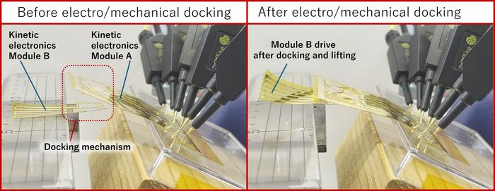
Side-by-side photos showing a pair of circuits before and after they connect
Come together: Kinetic electronics module A, which integrates an electrical circuit and an actuator, deforms in response to an electrical input and connects mechanically and electrically to thin-film circuit module B via the docking mechanism. Before connection (left image), the two modules are separate; after connection (right image), module A holds and lifts module B, and by supplying power through the connection point, it can independently drive module B to deform. (Courtesy: Fumihiro Sassa/Kyushu University)

Researchers at Kyushu University in Japan have developed a flexible electronic circuit that can connect itself to another electronic circuit and then disconnect from it. The prototype structure is an important step towards electronic devices that can reconfigure and even repair themselves, and it could have applications in wearable sensors, soft robotics and medical devices.

Most of today’s electronic devices are fixed, or “non-modular”, explains study leader Fumihiro Sassa of Kyushu University’s Department of Electrical and Electronic Engineering. Typically designed for specific tasks or environments, they are not readily adaptable to new ones, and they often cease to function if even a single component in their electronic circuitry fails. This leaves them dependent on human operators or external robotic systems if it becomes necessary to expand their functionality or repair damage.

“This can be a serious limitation inside very small machines, in space equipment, in devices requiring specialized handling, such as wearable chemical sensors, or in systems containing very large numbers of wires and electronic elements,” Sassa explains. “In such cases, in-situ repair can be difficult. The whole system may need to be replaced.”

Connection and disconnection

To overcome this problem, the Kyushu University researchers have been developing what they term “kinetic electronics” modules. These consist of electronic circuits and actuators that deform when an electrical current is applied to them so that they can mechanically and electrically connect to other modules. Before this connection takes place, different modules are separate, but after connection or “docking” takes place, one module can independently deform another when power is supplied through the point that connects them.

In this way, explains Sassa, the circuits can rearrange their own hardware structure. “Such functions have traditionally been used in mechanical systems, such as spacecraft, trains and modular robots, but we have now applied them to an electronic device.”

Sassa and colleagues fabricated their electrothermal bimorph actuators from polypropylene and polyimide films with heater electrodes and electrical circuits formed on them through a two-dimensional top-down process. Because the two polymers expand differently, Sassa explains that Joule heating causes selected actuator sections to bend. “Prescribed sequences of these motions produce docking and undocking and once docked, passive mechanical engagement maintains the connection without continuous power being supplied,” he says. “Undocking requires a separate actuation sequence.”

Towards miniaturization and more intelligent control

The researchers say they are working on miniaturizing their system and looking how to control it more intelligently. In the present study, which is detailed in npj Flexible Electronics, they demonstrated the docking mechanism using a small number of millimetre-scale independent sensors and actuators formed together on the circuit, with motion being controlled in sequence by an external microcontroller. They are now developing photolithographic processes to further decrease the size of these components and have already fabricated actuators smaller than 100 μm using these techniques.

“In a similar way to large-scale integration in conventional electronics, doing this will allow us to integrate very large numbers of these sensing and actuation elements, allowing the electronic circuit to form and change much more complex mechanical structures and functions,” says Sassa.

“We are also interested in so-called distributed control, in which the central controller does not need to specify every movement,” he adds. “Instead, many elements would follow relatively simple local control rules, from which advanced self-reconfiguration and self-organization could emerge.”

The post ‘Kinetic electronics’ make self-connecting circuits appeared first on Physics World.

❌