In a study published in Advanced Optical Materials, researchers at Vilnius University (VU) demonstrated perovskite-based laser structures that maintained stable performance over more than 400 million pulses. Their findings address one of the major challenges limiting the practical use of perovskites: their instability. These semiconductor materials could play an important role in next-generation optical technologies, but their tendency to degrade has long posed a challenge for researchers worldwide.
In a study published in Advanced Optical Materials, researchers at Vilnius University (VU) demonstrated perovskite-based laser structures that maintained stable performance over more than 400 million pulses. Their findings address one of the major challenges limiting the practical use of perovskites: their instability. These semiconductor materials could play an important role in next-generation optical technologies, but their tendency to degrade has long posed a challenge for researchers worldwide.
Despite being known for more mundane uses such as sticking notes to refrigerators or keeping bags shut, magnetization is one of the most fundamental and useful properties of a material. Indeed, it forms the physical basis for storing most of our digital information, encoding the bits used in hard drives, computer memories and credit cards.
In 2004, physicists isolated graphene, a sheet of carbon just one atom thick. It launched the study of two-dimensional (2D) materials: crystals a few atoms thick in which electrons are confined to a plane and can behave quite differently from those in ordinary solids. The family of known and predicted 2D crystals has since grown to thousands of members. Two recent studies show how computation can search that family for the most promising ones, the first for unusual electronic “topology”, the second for crystals well suited to twisting.
A hidden property of electrons
Electrons in a crystal can only have energies within allowed ranges called bands, separated by forbidden gaps. If a gap separates the filled electrons from the empty states, the material is an insulator. In a semimetal, filled and empty bands just touch, so a few electrons can move freely.
Two insulators can still differ at a deeper level, described by topology: a property of the whole set of electron states that cannot change smoothly, only by closing the gap or breaking a protecting symmetry. A doughnut and a coffee mug are topologically alike because each has one hole, and neither can become a sphere without tearing.
The idea took off with the quantum spin Hall effect. Proposed for graphene in 2005, it proved unobservable there because the effect is far too weak. A 2006 proposal for thin layers of mercury telluride was confirmed in 2007. In such a topological insulator the interior blocks current, yet the edges conduct, with electrons of opposite spin travelling in opposite directions, which protects them against many kinds of imperfection.
Symmetry-based methods known as topological quantum chemistry in 2017 made it possible to decide whether a computed electronic structure is topological. Applied to three-dimensional crystals, they pointed to thousands of candidates. Flat crystals lagged behind, with only about 400 known topological or related monolayers.
The first study, “Two-dimensional Topological Quantum Chemistry and Catalog of Topological Materials” 1, adapts these methods to 2D crystals and applies them to 8,872 entries in two computational databases. It finds 4,073 with nontrivial topology or a related property called obstruction, including 905 topological insulators, 2,129 topological semimetals and 1,003 obstructed atomic insulators, plus 36 close variants. In an obstructed insulator the electrons are centred on empty positions between the atoms rather than on the atoms themselves. The bulk looks ordinary, but cutting the crystal along certain lines produces edge states, and small flakes can carry fractions of an electron’s charge at their corners. The study also calculates edge states for selected materials. Its catalogue includes over 100 monolayers already made in laboratories, but most entries are computer predictions whose properties remain to be tested.
Workflow of the database construction. Starting from a 2D topological material database, a filtering score is applied to construct a database of theoretically twistable materials, which includes both semimetals and insulators. The candidate materials in this database are further classified according to their Bravais lattices, valley splitting, and spin splitting. Source: Y. Jiang et al. (2026) Science doi:10.1126/science.adu1550
Twisting layers
Stack two atomic sheets and rotate one slightly, and the mismatch creates a large interference pattern, called a moiré pattern, much like two overlapping window screens. Electrons feel this longer repeating pattern, and under the right conditions their bands become nearly flat. Electrons in a flat band have little energy of motion, so their mutual repulsion dominates and strongly correlated behaviour can emerge.
In 2011, calculations predicted that two graphene sheets twisted by about 1.1 degrees, a “magic angle”, would have such flat bands. In 2018, experiments at that angle revealed insulating states caused by electron repulsion, and superconductivity. Twisted layers of other materials, such as MoTe2 and WSe2, have since shown many correlated phases, though the mechanisms are still debated.
Most work has focused on these few materials, because most crystals have electronic structures too complicated to predict once twisted. The second study, “2D theoretically twistable material database” 2, therefore defines a material as theoretically twistable if its low-energy electrons admit a simple description. In a metal, the relevant electrons must sit at isolated points, as in graphene. In an insulator, the top of the filled band or the bottom of the empty band must stand clear of other bands. Insulators must also have gaps between 0.2 and 3 electronvolts, because larger gaps make electrical contacts difficult. The search was limited to crystals with at most 12 atoms in the repeating cell and four chemical elements.
Starting from the first study’s database, it identifies 61 semimetals and 1,568 insulators. It ranks them with a score and sorts them by lattice shape (about half are hexagonal), by where in momentum space the relevant electrons sit, and by the strength of spin-orbit coupling, the link between an electron’s spin and its motion. These choices shape the moiré pattern, which can resemble honeycomb, kagome or square lattices. Square-lattice moiré systems have been proposed but not yet realized, and could help simulate models relevant to cuprate superconductors.
Calculations on twisted bilayers of SnSe2, SnS2, ZrS2, HfS2 and Sc2CCl2 at a twist of about 7 degrees show isolated flat bands, as the database predicts. Experiments connect the theory to the laboratory. Bulk crystals of SnSe2, SnS2, HfS2, GaTe and ZrNCl were grown. Single layers of several candidates, including SnSe2, HfSe2, ZrS2 and WS2, were peeled off with a gold-assisted technique that yields larger, cleaner flakes. A dual-gated two-layer SnSe2 device was built for electrical measurements, and a twisted two-layer HfS2 device was used for scanning tunnelling measurements near absolute zero.
The direction is clear. Instead of discovering materials by trial and error, it is becoming possible to search systematically for crystals with chosen properties, then test them layer by layer.
Author: César Tomé López is a science writer and the editor of Mapping Ignorance
Disclaimer: Parts of this article may have been copied verbatim or almost verbatim from the referenced research paper/s.
References
U. Petralanda, Y. Jiang, H. Pi, M. G. Vergniory, B. A. Bernevig, N. Regnault, and L. Elcoro (2026) Two-dimensional topological quantum chemistry and catalog of topological materials Science doi: 10.1126/science.adu2107↩
Y. Jiang, U. Petralanda, H. Pi, G. Skorupskii, Q. Xu, D. Calugaru, H. Hu, J. Xie, R. A. Mustaf, P. Hohn, V. Haase, A. Ouahchi, S. Samal, J. Zhu, D. Yang, Z. Geng, G. Avedissian, Y. Wang, M. G. Vergniory, M. Claassen, et al. (2026) 2D theoretically twistable material database Science doi:10.1126/science.adu1550↩
In 1911, Heike Kamerlingh Onnes cooled mercury to a few degrees above absolute zero and watched its electrical resistance vanish. Lead soon joined the list of superconductors, losing its resistance below about 7.2 kelvin. A full explanation arrived in 1957: electrons bind into Cooper pairs that move together as one collective state below a critical temperature. Breaking a pair costs a minimum amount of energy, called the energy gap, so inside the gap a superconductor offers no states for single electrons.
Yu–Shiba–Rusinov states
Magnetism is an old enemy of this order. Magnetic impurities were known to suppress superconductivity, and in the 1960s Yu, Shiba and Rusinov showed theoretically that a magnetic atom disturbs the pairs around it and traps a localized state with an energy inside the gap. These Yu–Shiba–Rusinov (YSR) states were first seen atom by atom in 1997, using a scanning tunneling microscope (STM): a needle-sharp metal tip that measures the tiny current of electrons tunneling across a vacuum gap to a surface.
A different story concerns two superconductors joined by a very weak link. In 1962, Brian Josephson predicted that Cooper pairs can tunnel through such a link with no voltage at all, an effect confirmed in 1963. When a voltage is applied, another process takes over: multiple Andreev reflection. An electron whose energy lies inside the gap cannot enter a superconductor alone. Instead it is sent back as a hole, the absence of an electron, while a Cooper pair slips in, as Andreev described in 1964. Between two superconductors under a voltage V, a particle can bounce back and forth, gaining energy eV with each crossing, until it can finally escape above the gap. When n crossings are needed, the conductance shows a peak at a voltage equal to the sum of the two gaps divided by n. This pattern, explained in the early 1980s, is called subharmonic gap structure. For lead on lead the sum is 2.7 millivolts, so peaks are expected near 2.7, 1.35 and 0.9 millivolts.
A schematic of the scanning tunneling microscope junction. A lead-coated tip is approached to a nickelocene molecule (yellow) above a subsurface iron atom (red) on Pb(111). Source: C. Mier et al (2026) Nat. Commun. doi: 10.1038/s41467-026-76478-4CC BY-NC-ND 4.0
Impurity states and Andreev reflections have usually been treated as separate subjects. A recent experiment 1 places them in the same device. A nickelocene molecule, a nickel atom sandwiched between two five-carbon rings, sits on a lead surface above a single iron atom trapped between the molecule and the lead. On its own, the molecule carries a spin that appears as characteristic steps in the measured spectra. Above the iron, those steps vanish and YSR states appear instead. Density-functional calculations explain why: the magnetic moments of molecule and iron point in opposite directions and almost cancel, leaving a leftover spin of one half on the iron. That spin couples to the lead and produces a single pair of YSR states.
The second superconductor is a lead-coated STM tip, lowered toward the molecule at 2.4 kelvin. Far away, electrons tunnel through a wide vacuum barrier and the tip merely reads out the YSR states, which appear as lopsided peaks near the edge of the gap. As the tip approaches, the junction becomes more transparent, meaning electrons cross it more easily, and the setup becomes a weak link between two superconductors. At moderate conductance, new peaks appear at half the sum of the gaps, the signature of second-order Andreev reflection. At the highest conductances, a sharp peak develops at zero voltage: the Josephson contribution. Thermal fluctuations of the superconducting phase broaden this peak, as is typical of STM junctions.
These stages do not simply stack. As the tip approaches, the YSR peak moves to lower energy and mingles with the Andreev peaks. The interpretation is that the bound state becomes a stopping point along the Andreev path. Peaks then appear at the tip’s gap plus the bound-state energy, divided by n, rather than at the ordinary positions. This is called YSR-assisted multiple Andreev reflection.
Odd and even orders
A simple argument explains why odd and even orders differ. Each reflection carries the particle to the opposite electrode, and only the lead surface contains the magnetic atom; the tip has none. After an odd number of crossings the particle ends on the surface, where it can land in the bound state. The peak shifts and acquires the lopsided shape typical of tunneling into a single level. After an even number it ends in the tip, among ordinary states, and those peaks stay closer to their usual positions, although the second-order peak still turns lopsided at higher conductance as a YSR-assisted component splits off. Simulations reproduce this pattern. In the measurements, thermal broadening blurs finer details such as the third-order peak, and small features near zero voltage seem to reflect a mixture of both processes.
Reproducing the evolution of the spectra required two changes together: higher transparency and a stronger exchange coupling between the iron spin and the lead. Raising transparency alone gives a growth of the key peak that the measurements do not show. A likely reason is that the approaching tip slightly squeezes the molecule and strengthens the coupling, though this is an inference. The model treats the spin as classical and its two parameters as effective ones, so it is a phenomenological decomposition rather than a unique microscopic extraction. It also cannot capture the zero-voltage peak.
Even so, the result shows that YSR states and Andreev reflections are two limits of one problem, tuned continuously within a single molecular junction. Under suitable conditions, such spin-active links might also host a Josephson diode, in which supercurrent flows more easily in one direction, or a π-junction, in which the two superconductors prefer opposite phases. These remain possibilities, not demonstrated effects.
Author: César Tomé López is a science writer and the editor of Mapping Ignorance
Disclaimer: Parts of this article may have been copied verbatim or almost verbatim from the referenced research paper/s.
References
C. Mier, A. Fetida, R. Robles, P. Boronat, D. Jyoti, N. Lorente, L. Limot, and D. -J. Choi (2026) Yu-Shiba-Rusinov-assisted Andreev transport in a molecular junction between superconductors Nat. Commun. doi: 10.1038/s41467-026-76478-4↩
In the 1980s, scientists measured quantized jumps in the energy of ions for the first time. In the 2000s, it was photons’ turn. Now, thanks to a tour de force of device engineering and nanofabrication, researchers at Stanford University in the US are reporting that phonons – mechanical vibrations like those that carry sound – also display this quantum behaviour.
“We could see it by eye [in the data], which was very satisfying,” team leader Amir Safavi-Naeini tells Physics World. “I’ve been fascinated with the interface between the quantum world and the classical world and trying to move that interface closer to daily experience…and now we have mechanical objects.”
Laying the groundwork
The Stanford team’s recipe for observing quantum jumps in phonons begins with thin films of lithium niobate (LiNbO3). Although bulk samples of this material had been available since the 1950s, the commercialization of thin-film LiNbO3 a decade ago was a game changer for Safavi-Naeini and his colleagues once they worked out how to process the material.
Because LiNbO3 is piezoelectric, placing it under stress – from a vibration, say – produces a voltage. This voltage allows vibrational quanta to couple to superconducting qubits, after which the qubit states can be “read out” to determine whether a phonon was present or not.
The problem was that initially, the phonons had lifetimes of only 800 nanoseconds – well short of the millisecond the team needed to observe them falling from an excited state to the ground state. Extending these phonon coherence times “took a lot of work by a number of graduate students in my group,” Safavi-Naeini says.
After probing various sources of dissipation, including material properties that cause quantum excitations to lose coherence, the researchers realized that surface defects were key offenders. They therefore switched from polymer processing, which left a residue, to shadow masks that superimpose one chip over the other and evaporate metal through it. “There were probably three generations of students that worked on getting that four to five orders of magnitude increase in the performance of the devices,” Safavi-Naeini says.
The voltage profile of the nanomechanical resonator in motion. In the crystal used for the mechanical resonator, mechanical motion and electrical potentials are inherently coupled, so the motion profile has an accompanying electric potential profile. (Courtesy: Erik Szakiel)
Once they’d extended their phonon lifetimes, the researchers had to find a way of combining their “very clean, long-lived” mechanical and superconducting systems without destroying either. For this, Safavi-Naeini credits past and present students Takuma Makihara and Erik Szakiel, who spent most of their PhDs tackling issues with the mechanical oscillators before finding a way to couple them to the superconducting systems. “That was the last piece,” Safavi-Naeini recalls. “Once we had that, we could do these experiments.”
Spot the missing phonon
Because the superconducting qubits detect whether an even or odd number of phonons is present in the LiNbO3 (which at very low energies amounts to determining whether a phonon is there at all), they are effectively performing a parity measurement. That could make the Stanford team’s system useful for quantum error correction, where the goal is to find out whether an error has crept in without actually measuring the quantum states, since doing so would destroy their useful quantum characteristics.
One of the most common sources of error in superconducting qubits is the loss of an excitation, such as when a phonon decays. However, if data is encoded into phonons in pairs and the system detects an odd number of them, this loss becomes apparent without measuring all the states. This so-called “binomial” code has already been implemented for microwave photons, and Safavi-Naeini explains that it works best for long-lived particles – a further benefit of the team’s long-lived phonons.
Protein and gravity measurements
The Stanford researchers are now collaborating with Michael Roukes and colleagues at the California Institute of Technology (Caltech) to explore possible applications in high-precision measurements of single protein masses. They are also interested in fundamental science questions such as whether it’s possible to generate entanglement between mechanical systems through gravitational fields.
However, Safavi-Naeini cautions that their phonon lifetimes would need to be much longer – a factor of 10 for error correction and mass spectrometry, and for gravity perhaps as much as six orders of magnitude, with further modifications to the experimental set-up also required – before they can achieve these goals. “The hope is that by figuring out the fundamental sources of loss in these materials we can build our way up to those experiments in the coming decade,” he says. “Every time you improve, you hit some new source of noise, you understand it, then you can deal with it, and then you go to the next one. It’s a fun physics problem.”
In the mid-1970s a graduate student wrestling with a deceptively simple quantum problem uncovered one of the most haunting images in modern physics. The pattern seemed almost impossibly intricate: delicate wings assembled from infinitely nested bands and gaps, a self-similar pattern born from the motion of electrons in a crystal under a magnetic field. First published in 1976 (Phys. Rev. B14 2239), it came to be known as Hofstadter’s butterfly, after its discoverer Douglas Hofstadter.
Half a century later, the butterfly has not faded into scientific nostalgia. If anything, it has become even more important – reappearing in new materials, new experiments and in places no-one imagined when it was first plotted. Recent research by Kazuki Ikeda from the University of Massachusetts and Yaron Oz at Stony Brook University suggests that related patterns may even surface in the physics of black holes (J. High Energy Phys.2026 38).
Each new realization adds another chapter to a story that is not really about a single graph, or even a single discovery, but about the unity of patterns across the physical world. A structure first seen in a simple model has become a symbol of how richness can emerge from basic rules, how beauty can arise from constraint, and how the quantum world still harbours forms strange enough to surprise us.
How the butterfly got its wings
What makes Hofstadter’s butterfly so compelling is the remarkable story of its birth and, more importantly, how far it has travelled from its original birthplace. Like many scientific breakthroughs, its discovery was fairly obscure initially and owed a great deal to luck. In 1974 Hofstadter – son of the 1961 Nobel-prize-winning nuclear physicist Robert Hofstadter – had just dropped out of graduate school at Stanford University in the US and was “in despair” according to friend and physicist Francisco Claro.
Having just completed a PhD with the renowned solid-state physicist Gregory Wannier at the University of Oregon, Claro suggested that Hofstadter should approach Wannier as well. As it happened, Wannier had been struggling with a problem that had puzzled him for years: he could not obtain an analytical solution to Harper’s equation, which describes the motion of electrons on a 2D crystal lattice subjected to a perpendicular magnetic field.
Named after P G Harper, who was a graduate student of Rudolf Peierls at the University of Birmingham, UK, this classic “magnetic problem” displayed a mysterious sensitivity to whether the magnetic flux was a rational or irrational number. It was a feature that immediately captured Hofstadter’s imagination and, with the rational–irrational dichotomy echoing in his mind, Hofstadter began his PhD studies at Oregon by immersing himself in solving the problem.
But he soon found himself equally stuck. Frustrated by the analytical approaches often discussed at the time, he pursued a different path: numerical computation. Using a programmable Hewlett Packard desktop calculator that by today’s standards looks laughably primitive, he displayed the numerical solutions graphically as the energy of electrons versus magnetic flux Φ per unit cell of the lattice. At that moment, he became convinced that he had uncovered the true structure of the problem. “All at once my eyes were opened,” Hofstadter recalls.
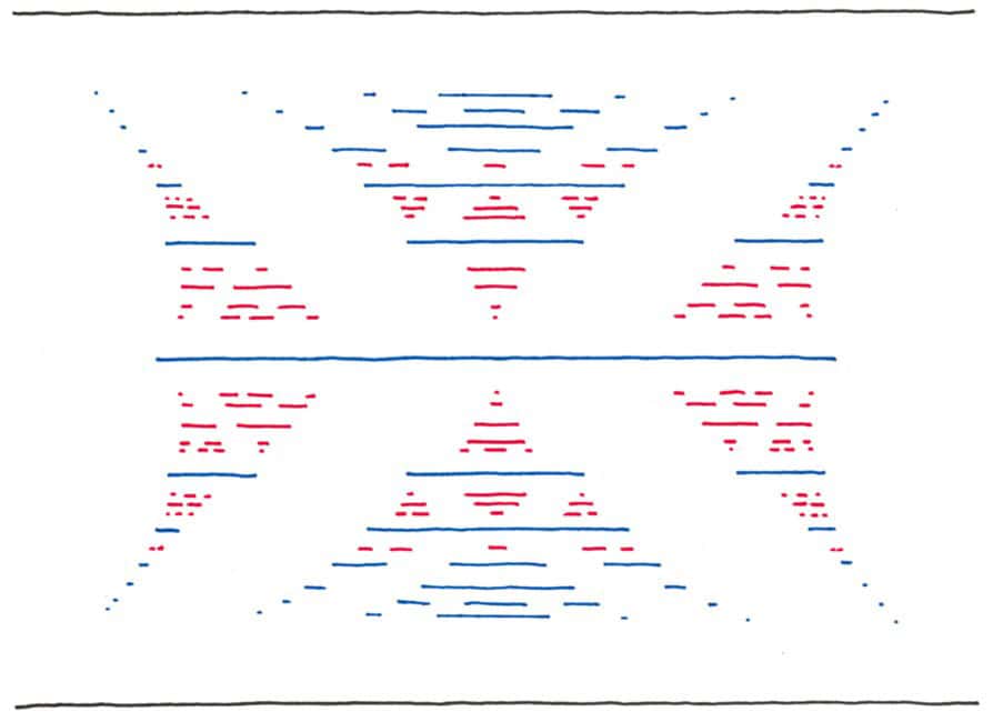
Beautiful beginning Hofstadter’s butterfly dates back to November 1974 when Douglas Hofstadter, who was then a PhD student at the University of Oregon, was trying to describe the motion of electrons in a 2D crystal lattice under an applied magnetic field. His work led him to produce a primitive, hand-drawn diagram – dubbed “Gplot” – that looked like a butterfly. The original diagram has been lost so Hofstadter created this reconstruction in 2016. (Courtesy: Indu Satija. Permission granted by Douglas Hofstadter)
What he found was a complex recursive shape (or fractal in today’s terminology) hidden within the energy spectrum of electrons in a magnetic field. Resembling a butterfly, Hofstadter brought his hand-plotted diagram, which he codenamed “Gplot”, to Wannier, who was not impressed. According to Hofstadter, Wannier dismissed the result as “numerology” and even threatened to withdraw the PhD student’s funding.
But after nearly a year, Wannier came to recognize the validity and significance of Hofstadter’s work, ultimately awarding Hofstadter his PhD and accepting the butterfly as a legitimate description of the energy spectrum of electrons moving on a 2D lattice in a magnetic field. Wannier even added to the butterfly’s story with a paper titled “A result not dependent on rationality for Bloch electrons in a magnetic field (Phys. Status Solidib88 757). This work, along with further studies with Claro, introduced a set of integers uniquely labelling every gap in the graph, providing a simplified description of the spectrum (Phys. Rev. B 19 6068).
Douglas Hofstadter: in his own words
Ruby celebration Douglas Hofstadter (right) pictured in 2016 with colleagues Indu Satija (centre) and Francisco Claro (left) all wearing T-shirts emblazoned with Hofstadter’s butterfly to celebrate its 40th anniversary. (Courtesy: Indu Satija)
Born in 1945, Douglas Hofstadter discovered his eponymous butterfly while a PhD student at the University of Oregon in 1975, using computational modelling to make his breakthrough (see main text). Four years later Hofstadter published his Pulitzer-prize-winning popular-science book Gödel, Escher, Bach, which tackles cognition, mathematics and symmetry.
Currently a professor of cognitive science and comparative literature at Indiana University in Bloomington, US, Hofstadter is still active as a researcher and wrote a follow-up book I Am a Strange Loop in 2007. On the golden jubilee of the now-famous butterfly named after him, Hofstadter provided the following comment to Physics World.
“This graph was first computed using a programmable desktop calculator and was first plotted by hand using coloured felt-tip pens. I was just extremely relieved that by showing that my ‘Gplot’ graph was made of distorted copies of itself, I would at last be able to get a PhD thesis. I had no idea that Gplot would go on to become well known as the Hofstadter butterfly, and that variations on the theme would proliferate like wildfire over the coming decades.”
“As the years have gone by,” he continues, “articles about Hofstadter’s butterfly have grown more and more numerous and harder and harder for me to follow. For better or for worse, these theories are all way beyond me, but remembering the first wingbeats of the butterfly’s flight cheers me up.”
Statements about states
Hofstadter’s butterfly is more than a beautiful graph. It is a map of what happens when quantum particles are caught between two competing kinds of order: the regular periodicity of a crystal lattice and the circular orbits of a magnetic field. When these two scales contend with one another, the energy spectrum does something extraordinary. Instead of varying smoothly, it fragments into a hierarchy of allowed and forbidden energies, referred to as bands and gaps, respectively.
Zoom in on one region and new structures emerge. Zoom in again and the pattern repeats, endlessly varied yet ruled by strict mathematical order. It is one of the rare instances in which fractal geometry appears not only in abstract mathematics or artistic imagination, but in the measurable behaviour of matter itself.
The deep connection between this theoretical pattern and real-world matter became clear through an exotic quantum phenomenon known as the integer quantum Hall effect. It was discovered experimentally by Klaus von Klitzing at the Max Planck Institute for Solid-State Physics in 1980 – a breakthrough that earned him the Nobel Prize in Physics five years later.
The classical Hall effect is what happens when a voltage is produced in a bulk conductor at right angles to an applied magnetic field. Similarly, the quantum Hall effect is the appearance of a voltage across opposite faces of a thin 2D semiconductor when a current is passed along the plane of the material and a magnetic field applied perpendicularly it. But there is one big difference in the quantum version.
If you slowly increase the power of the magnet, the transverse electrical conductance does not grow steadily. Instead, it jumps up sharply, with plateaus in between like steps on a staircase. In other words, it assumes quantized values given by integer multiples of the fundamental constant e2/h, where h is Planck’s constant and e is the charge on an electron.
In 1982 the British physicist David Thouless and his collaborators at the University of Washington, Seattle, made another remarkable discovery: the effect, they found, is topological. Topology is the study of the global properties of objects and topological invariants are those properties that do not change regardless of how much you try to deform a given object.
Thouless and colleagues found that the integers underlying the quantum Hall effect are topological invariants arising from the global topology of the electronic wave functions. This seminal work, which was published in 1982 (Phys. Rev. Lett.49 405), significantly contributed to Thouless earning the 2016 Nobel Prize in Physics, which he shared with Duncan Haldane and Michael Kosterlitz for their work on “topological phase transitions and topological phases of matter”.
1 Butterfly behaviour
(Courtesy: Indu Satija; CC BY 3.0 New J. Phys.18 103023; J. Stat. Phys. 156 417. Reused with permission from Springer Nature)
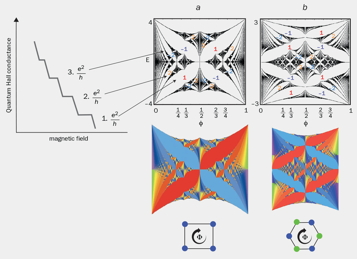
Hofstadter’s butterfly, in its original form, refers to the behaviour of electrons in 2D lattices subject to an applied magnetic field. (a and b) Shown here (top row) are graphs of the electrons’ energy (E) plotted against the magnetic flux (Φ) per unit cell for square and honeycomb lattices (bottom row). The relation between the quantum Hall effect (displayed in the staircase-like graph, left) and Hofstadter’s butterfly is shown via the arrows. The colours on the “butterfly graphs” (middle row) correspond to the quantum numbers of the Hall conductivity. Some of these integer labels are shown (colour coded) in the top row.
How all of this relates to Hofstadter’s butterfly is simple: the butterfly model describes all integer quantum Hall states, where the integers of Hall conductivity label the gaps in Hofstadter’s butterfly – the exact same integers that Wannier and Claro introduced in the butterfly spectrum (figure 1). In other words, the butterfly is not merely a chart of recursively split energy levels; it is also a coded map of topology in quantum matter under a magnetic field.
A pattern repeating across physics
That connection places it squarely within one of the central themes of modern condensed-matter physics, namely the realization that certain physical properties are protected not by local details, but by global features of the quantum state. But what is fascinating is that in the 50 years since Hofstadter’s butterfly was discovered, physicists have found that the same spectral architecture in it can also arise in a remarkable range of settings. It has appeared, for example, in other lattice geometries, in engineered semiconductor devices and in so-called moiré materials.
The butterfly’s migration into moiré systems has been especially fruitful. Such materials are created by stacking two atomically thin materials onto each other with a slight twist, creating a moiré pattern with different properties from the individual layers. Utilizing moiré materials, in research that began in 2013 led by Philip Kim of Columbia University (Nature497 598) and continues apace with a team led by Ali Yazdani of Princeton University (Nature639 60), the butterfly structure can now be tuned, probed and in some cases directly imaged on modern quantum platforms.
Over the last 50 years, the butterfly itself has also evolved into other forms. For instance, in some systems, the butterfly emerges without an external magnetic field. As a team of researchers led by Xu-Tao Wan from East China Normal University showed in 2025 (Phys. Rev. Lett.136 033401), the fractal pattern can be controlled by twist angle – that is, by geometry alone.
Each time physicists add a new layer of realism – spin, interactions, periodic driving or lattice complexity – the butterfly adapts, and re-emerges in new forms, so long as it is not overwhelmed by strong interactions, disorder or thermal effects
In other realistic systems, electron spin – the particle’s intrinsic magnetic orientation, absent from the original simplified model – becomes an essential part of the physics. Even when a magnetic field splits the system into spin-up and spin-down states via Zeeman splitting, the butterfly spectrum survives. More striking still, the butterfly can emerge independently for each spin state, as Xiaomeng Liu and Zhida Liu of Cornell University discovered in 2025 (Nature Phys.21 1873).
This persistence of the fractal structure, despite the added complexity introduced by spin, highlights the extraordinary robustness and universality of the underlying quantum phenomenon. More generally, what these new iterations of Hofstadter’s butterfly reveal is that what once looked like a specialized theoretical curiosity now seems more like a recurring motif in quantum matter.
Indeed, this is part of its enduring fascination: each time physicists add a new layer of realism – spin, interactions, periodic driving or lattice complexity – the butterfly adapts, and re-emerges in new forms, so long as it is not overwhelmed by strong interactions, disorder or thermal effects. This durability prompted a friend to once joke that whenever he undergoes an MRI scan, he cannot help wondering what kind of butterfly his body might be producing.
Beauty from simplicity
As my friend’s joke reveals, there is something unmistakably human about the butterfly’s appeal. Physicists are drawn to it not only for its usefulness, but for its beauty. It belongs to that rare class of scientific objects whose visual grace seems to gesture toward deeper truths. And yet its deepest charm may lie in the fact that its immense complexity grows from remarkable simplicity.
2 Baby butterflies
(Courtesy: Indu Satija)
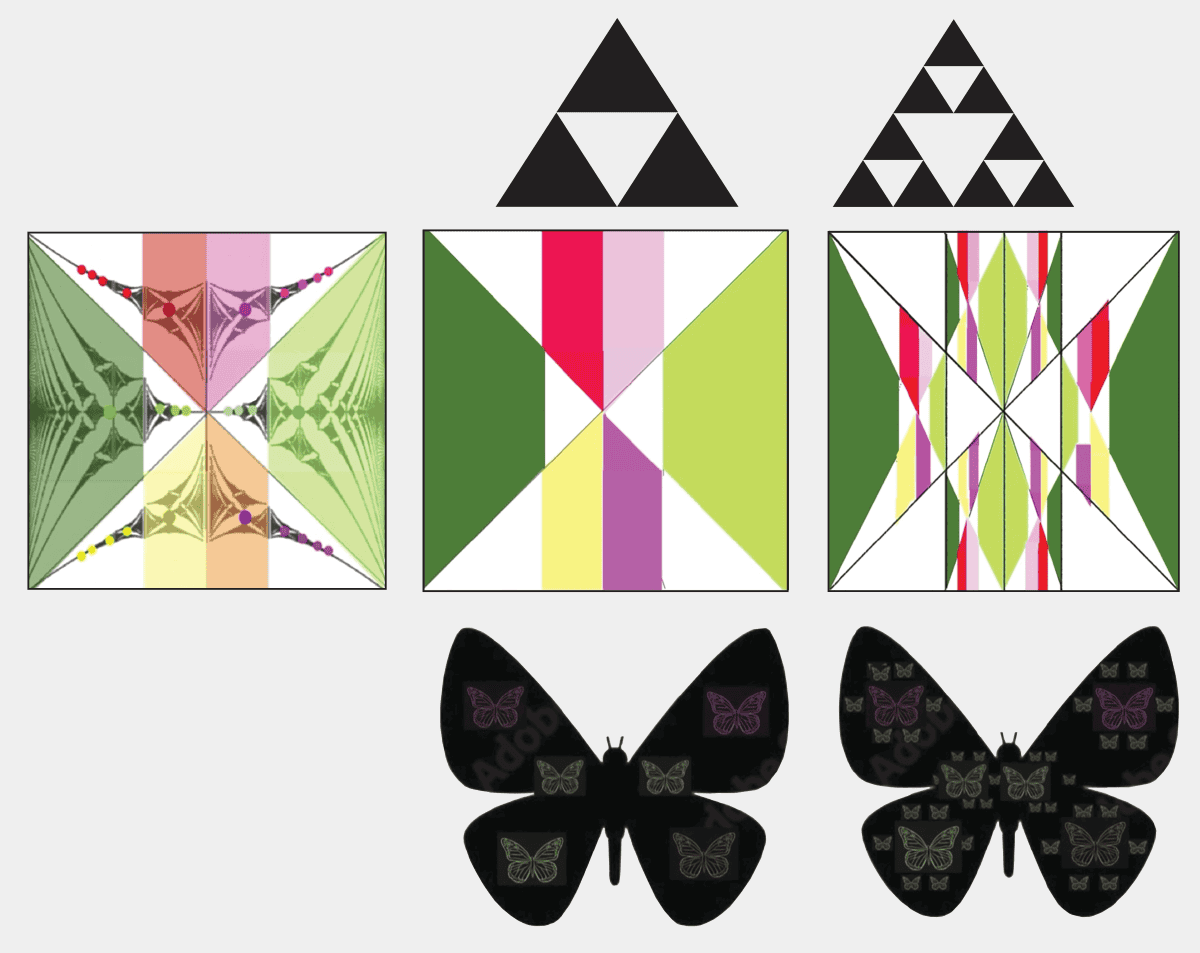
A simplified representation of Hofstadter’s butterfly, commonly known as the butterfly skeleton, interpreted as a 2D tessellation of trapezoids and triangles. It is shown in parallel with the “Sierpiński gasket” (top), which is made entirely from triangles. The iterative construction underlying this fractal consists of a parent butterfly generating six “baby” butterflies, represented by the six colour-coded trapezoids. Each baby butterfly is accompanied by a tail – an infinite chain of progressively smaller butterflies, indicated schematically by dots in the corresponding colour. The two butterflies at the bottom provide a schematic illustration of the hierarchical organization of the structure.
Beneath the intricate pattern are integers, recursion relations and number-theoretic structures that connect it to fairly simple geometric patterns, including the Farey tree, the tree of Pythagorean triplets and fractal packings such as the Apollonian gasket. In fact, this complicated quantum fractal admits a surprisingly simple geometric description: the butterfly landscape can be organized as a hierarchical lattice of trapezoids, bringing it into close parallel with geometric fractals such as the Sierpiński gasket (figure 2). It is extraordinary to think that this geometric harmony underlies such a complex and beautiful graph.
Fifty years on, Hofstadter’s butterfly remains exactly what great scientific ideas are supposed to be: elegant, prolific and unfinished. That interplay of beauty, mathematics and physical reality is what keeps the butterfly alive. Its evolution under interactions, spin effects and new forms of engineered geometry continues to reveal unexpected physics. And with each turn, the butterfly reminds us of something rare and precious in science: that the universe can hide immense complexity within simple forms, and that sometimes, if we are lucky, those forms are beautiful enough to be unforgettable.
Multiferroics are materials that simultaneously exhibit two or more ferroic orders—stable arrangements of physical properties that can be switched using an external stimulus. These materials could be highly advantageous for the development of various technologies, including non-volatile, low-power memory devices, spintronic devices, miniaturized electronics, neuromorphic hardware, sensors and magnetoelectric devices.
When a material heats up, its electrical resistance often rises. The harder question is what, exactly, is getting in the way. The electrons carrying the current may be scattered by vibrations of the material's atomic lattice, known as phonons. They may also collide with one another. Frustratingly, a conventional temperature test warms the electrons and the lattice together, so the effects arrive tangled in the same resistance measurement.
When a material heats up, its electrical resistance often rises. The harder question is what, exactly, is getting in the way. The electrons carrying the current may be scattered by vibrations of the material's atomic lattice, known as phonons. They may also collide with one another. Frustratingly, a conventional temperature test warms the electrons and the lattice together, so the effects arrive tangled in the same resistance measurement.
Nickel disulfide, NiS₂, is an unusual material. Its interior behaves as an electrical insulator, blocking the flow of current, while certain parts of its surface conduct electricity freely. This contradiction has puzzled physicists for decades, and a recent study offers a detailed explanation. The conduction, it turns out, is confined to tiny one-dimensional steps on the surface, and these narrow conducting channels are a direct consequence of how electrons are arranged inside the crystal.
Mott insulator
NiS₂ shares its crystal structure with pyrite, the mineral sometimes called fool’s gold. At ordinary conditions, its electrons do not move freely through the lattice: the strong electrical repulsion between them opens an energy gap that keeps the bulk of the material insulating. This behaviour defines what physicists call a Mott, or charge-transfer, insulator, a category of materials that simple band theory cannot explain. Band theory predicts that any material with a partially filled outer electron shell should conduct electricity, yet compounds like nickel oxide obstinately insulate instead. In 1949, the physicist Nevill Mott showed why: if two electrons crowding the same atomic site cost more energy than is available, the electrons stay locked in place and no current flows, regardless of what band theory predicts. NiS₂ behaves in much the same way.
Yet electrical-transport measurements had repeatedly found that crystals of NiS₂ conduct through their surfaces. Earlier scanning-tunnelling experiments helped explain part of the puzzle: the broad, flat surface remains insulating, but the electronic gap narrows sharply near atomic-scale steps, tiny cliffs just one or two atoms high where the surface abruptly changes level. A new study 1 confirms this picture and examines the steps with much higher spatial resolution than before.
A not that smooth surface
A scanning tunnelling microscope (STM) works by bringing an extremely sharp needle close enough to a surface that electrons can leak across the gap between tip and sample. Measuring that leakage at different energies reveals both the surface’s shape and how easily electrons can enter or leave it. In NiS₂, these measurements uncovered electronic states concentrated tightly along the step edges: the states extend for a long distance parallel to a step but stay confined to roughly one to two nanometres across it. In other words, the electrons are effectively free to move in one direction while remaining trapped in the other two, forming genuine one-dimensional conduction channels.
Surface spectra of the terminations observed in STM. Source: M. Iraola, H. Guo et al (2026) Nature Communications doi: 10.1038/s41467-026-76126-x
Two distinct kinds of surface step were observed, depending on whether the outermost atomic layer exposes nickel or sulfur atoms. Both carry electronic states associated with their steps, but they are not equally important. The nickel-terminated steps host states that sit right at the energy where electrical conduction happens, making them the most likely explanation for the surface conductivity that transport experiments had measured for years. The sulfur-terminated steps also host states inside the insulating gap, but their energy is positioned further away, making them less directly responsible for carrying current.
The study also tested what happens when a magnetic field is applied perpendicular to the surface. The step-edge states survived fields as strong as 10 tesla, a field far stronger than any produced by a laboratory magnet used for everyday purposes. Their intensity weakened somewhat, particularly on the sulfur-terminated steps, but the states were never destroyed. This robustness matters because NiS₂ already displays complicated magnetic behaviour of its own, which might easily have disrupted a more fragile conducting state.
The deeper explanation lies in how electrons are distributed inside the crystal. In an ordinary insulator, the occupied electronic states can usually be pictured as clouds centred on the atoms themselves. NiS₂ is different: calculations show that part of its electron density is naturally centred at special positions between atoms, specifically near the midpoints of pairs of sulfur atoms, where no atom actually sits. Physicists call these obstructed charge centres, and materials built around them belong to a class known as obstructed atomic insulators, a concept that grew out of a broader effort over the past decade to classify materials by the geometry, and not just the energy, of their electron states.
The concept of obstructed atomic insulator. In an OAI, the valence bands are induced from Wannier functions localized at obstructed Wannier charge centers (OWCCs)—symmetric positions in the crystal not occupied by any ion. Wannier functions are the localized molecular orbitals of crystalline systems. Source: M. Iraola, H. Guo et al (2026) Nature Communications doi: 10.1038/s41467-026-76126-x
Not ordinary metallic defects
This arrangement is not a chemical accident; it is protected by the symmetry of the crystal. When the crystal is cut to form a surface, though, the special positions that hosted this electron density can no longer fit together the way they did in the bulk. At a step edge, this mismatch creates what is known as a filling anomaly: an imbalance in how the available electronic states can be occupied, which leaves behind a state inside the insulating gap, localized right at the edge. Calculations of artificial step structures reproduce the main features seen under the microscope, including this localization, supporting the idea that the conducting channels are not ordinary metallic defects caused by broken chemical bonds, but a direct consequence of the crystal’s underlying electronic geometry.
The study also settles a long-standing question about NiS₂’s magnetism at low temperature. Below about 39 kelvin, the nickel magnetic moments arrange themselves into a non-collinear antiferromagnetic pattern, with neighbouring moments pointing in different directions that largely cancel out. Below about 30 kelvin, they rearrange again into a state that produces a small but measurable net magnetization. New neutron-diffraction measurements support a revised model of this low-temperature arrangement, resolving a debate about the material’s magnetic ground state that had lasted for roughly fifty years.
Taken together, the results give NiS₂ a significance well beyond its peculiar conducting surface. The material shows that strong repulsion between electrons, magnetism, and the geometry of electronic states can coexist within a single crystal. Such geometric protection is normally associated with topological materials, in which certain electronic states are shielded from disorder or defects by the crystal’s symmetry. The new results suggest that this protection can survive even when strong interactions push a material into being an insulator, making NiS₂ a rare setting for studying how the quantum-mechanical arrangement of electrons decides where electricity is allowed to flow within an otherwise insulating crystal.
Author: César Tomé López is a science writer and the editor of Mapping Ignorance
Disclaimer: Parts of this article may have been copied verbatim or almost verbatim from the referenced research paper/s.
References
Mikel Iraola, Haojie Guo, Fabio Orlandi, Sebastian Klemenz, Martina O. Soldini, Sandra Sajan, Pascal Manuel, Jeroen van den Brink, Titus Neupert, Miguel M. Ugeda, Leslie M. Schoop & Maia G. Vergniory (2026) One-dimensional conduction channels in the correlated Mott NiS2 arising from obstructed Wannier charges Nature Communications doi: 10.1038/s41467-026-76126-x↩
Topological quantum materials combine unusual electronic states with properties such as magnetism or superconductivity, offering possibilities for future electronics and quantum technologies. Researchers at Tohoku University have now shown that changing the number of layers in a crystal can provide a systematic way to design topological magnets. The work is published in the Journal of the American Chemical Society.
Topological quantum materials combine unusual electronic states with properties such as magnetism or superconductivity, offering possibilities for future electronics and quantum technologies. Researchers at Tohoku University have now shown that changing the number of layers in a crystal can provide a systematic way to design topological magnets. The work is published in the Journal of the American Chemical Society.
Material properties such as sound insulation, resistance to extreme heat and thermal expansion originate from how the zillions of microscopic building blocks (nuclei and electrons) interact at equilibrium and respond to perturbations. Atoms are typically about one ten-billionth of a meter across, so there can be a lot of parts to keep track of—a task that is complicated at the quantum-mechanical level, where particles are neither here nor there until observed.
Material properties such as sound insulation, resistance to extreme heat and thermal expansion originate from how the zillions of microscopic building blocks (nuclei and electrons) interact at equilibrium and respond to perturbations. Atoms are typically about one ten-billionth of a meter across, so there can be a lot of parts to keep track of—a task that is complicated at the quantum-mechanical level, where particles are neither here nor there until observed.
Researchers at Nagoya University have built a graphene nanoribbon that can switch which way it twists using a natural solvent. Graphene nanoribbons are thin ribbon-shaped structures made of fused carbon rings. Twisted or helical versions of these ribbons show promise for advanced light and electronic devices. However, no graphene nanoribbon could switch that twist on demand, until now.
A 3D illustration of the [4]helicene nanoribbon shows the long chain of fused rings that gives the molecule its twisted structure. Source: Tomoyuki Ikai / Nagoya UniversityScientists have worked out how to switch between a right-handed and left-handed twist (chirality) by changing the solvent around it. The discovery 1 opens opportunities for new optical switches, chemical sensors, and spintronic components that adapt to changing environments.
Tomoyuki Ikai, lead author and professor at Nagoya University’s Graduate School of Engineering, is a polymer chemist inspired by natural helical structures such as DNA and proteins. Polymers are large molecules built from many small, repeating units linked together in a chain. Ikai had been working on ladder polymers, where each repeating unit is locked into place and cannot freely rotate around the bond connecting to its neighbor (unlike a typical flexible linear polymer).
“We used the same fusion approach already used to make predictable helical ladder polymers. But instead of a stable building block, such as [6]helicene, we used [4]helicene, a 4-ring unit written off as too unstable to be useful,” Ikai said.
Soak, twist, repeat
These units are difficult to control on their own because they switch their chirality too fast to hold one handedness. The team’s method fuses these small, restless units into one long chain. Once joined, they found that a neighbor effect took hold: each unit’s twist began to match its neighbors, and long stretches of the ribbon settled into a single, shared spiral.
To lock it in one overall direction, the researchers dissolved the ribbon in a natural chiral liquid, a liquid made of molecules that come in two mirror-image versions. They tested six candidates before they found the right one: beta-pinene, a compound found in pine trees and citrus peel.
Because beta-pinene molecules can be arranged in left- and right-hand mirror-images, these two versions each push the ribbon toward the opposite spiral. This also changed the twist direction of light the ribbon gave off, a property called circularly polarized luminescence, and is the first graphene nanoribbon shown to switch its light this way.
The switching induced a remarkably high degree of helical bias, with almost all of the helicene units aligning in the same direction. The switching effect is strongest at –90°C and grows weaker as the temperature rises toward room temperature.
“For a long time, people saw [4]helicene as unsuitable for chiral materials, because it could not be controlled,” Ikai said. “In this paper, we show that once you link enough of these units together, the instability itself becomes the useful part.”
A chiral solvent’s nudge toward one handedness is usually very weak on its own. Here, the ribbon’s own structure, with each unit mechanically linked to its neighbors, amplifies that weak nudge into a strong, nearly one-handed result.
An adaptive material
The researchers point to several possible future uses: The switchable light could serve optical devices. The ribbon’s chemical sensitivity to beta-pinene suggests it may work as a chiral sensor, and a similar design could one day help detect hazardous or unstable chemicals. Because graphene conducts electricity well, the ribbon may also suit electronic sensors.
The molecule’s twisted shape connects to spintronics, a field that uses the spin of electrons rather than just their charge. Ikai noted that a right-handed or left-handed structure can, in principle, let electrons of one spin pass through more easily than the other, a property helical structures are known for in physics literature.
The current design only holds its twist while it stays in the chiral liquid. If the solvent is removed, the ribbon drifts back to a mixed, unstable state. Ikai’s next goal is a form of “chiral memory,” a way for the ribbon to lock in its twist even after the solvent is gone. This next step builds on memory techniques the researchers have explored in other helical systems and is now applied to graphene for the first time.
References
Ikai, T., Inagaki, H., Oki, K. et al. (2026) Dynamic helical poly[4]helicene nanoribbon. Nat Commun doi: 10.1038/s41467-026-76724-9↩
Water droplets sliding across solid surfaces can acquire electric potentials of thousands of volts and thereby corrode non-conductive surfaces on metals when they discharge. That is the conclusion of researchers in Germany who say that the poorly-understood phenomenon warrants further investigation to help prevent corrosion of vulnerable outdoor equipment and cultural heritage sites.
Metal corrosion by water droplets is a serious economic and safety issue, and prevention begins with the proper understanding of the relevant processes. Conventional wisdom is that most corrosion is caused by a combination of physical abrasion by the motion of the droplets and chemical degradation from natural acids and anthropogenic pollutants in the water. The notion that electrochemistry might play a significant role in corrosion had not been seriously considered, says physical chemist Hans-Jürgen Butt of the Max Planck Institute for Polymer Research in Mainz.
Part of the reason, he believes, is that, until relatively recently, it was thought that the triboelectric effect (electrically charging objects by rubbing them together) did not work in liquids. “If you have a solid and you rub another insulating solid against it you get electron transfer – I think this has been known for more than 2500 years” he says. However, this relies on atomic-scale roughness of the surface to concentrate charge at specific points where bonds can be broken – and fluids cannot, by definition, be rough.
“If you take a water droplet and let it slide there is some mechanical force from surface tension, but that’s much too low,” says Butt. “There is no way you could generate enough energy locally to pick up an electron or to put an electron or an ion from the water onto the surface.” In the past 10 years, however, it has become increasingly clear that sliding droplets do become highly charged.
Sloping surfaces
In their present work Butt and colleagues deposited water droplets onto copper surfaces covered with 60 nm of Teflon. When they dropped droplets straight onto the surface, they observed no corrosion. They then deposited droplets first onto a variety of other sloped insulating surfaces such as plant leaves, PVC construction boards and the perfluorooctadecyltrichlorosilane (PFOTS) hydrophobic coating often used on window glass. The droplets ran down these surfaces and then fell onto the Teflon-coated copper. After around 3000 droplet impacts, atomic force microscopy and confocal microscopy revealed evidence that the droplets had corroded both the coating and the underlying copper.
The researchers believe that the droplets become positively charged as they slide down the sloping surface. As they fall onto the coating, the potential difference between the copper and the underlying copper can exceed 1 kV. This is greater than the dielectric breakdown strength of the coating, causing the droplet to discharge. This damages the coating and leaves the underlying metal vulnerable to further oxidation.
To test their hypothesis, the researchers measured charge movement within the copper surface, showing that negative charge flowed towards droplets dripping off insulating surfaces. They also used high-speed cameras to show that, whereas a drop deposited directly retained its spherical shape before impact, a dripping drop was drawn into a cone shape, producing a tip of positive charge that would increase its corrosive capacity.
Uncertain consequences
The practical implications of this are unclear. “Technical coatings on cars, ships etc. are typically 100 microns and thicker, so the process we describe is probably not of direct relevance,”says Butt. However, the phenomenon could be involved in the degradation of monuments and other outdoor historical objects. “We have evidence that surfaces change their properties when you slide charges over them, but the real consequences are not yet known,” explains Butt.
He says his own group is most clearly focused on understanding the fundamental physics involved. “We still don’t know why the heck there is such a charge separation: it’s energetically unfavourable, it should not happen, but it happens.” he says. “The one effect we describe here is, in a way, pretty trivial – everyone knows that if you have a high potential and it’s somehow grounded there is a breakthrough – but what happens at the surface with this deposited charge is not clear.”
Materials scientist Zhong Lin Wang of Georgia Institute of Technology in Atlanta was one of the first researchers to discover the triboelectric effect in liquids, and helped to develop the triboelectric nanogenerator used to quantify it. “The transferred electrons can be kicked back to the water solution, resulting in chemical reaction at the vicinity surface. This process, called contact-electro-catalysis, was first proposed in 2022, and is now an active field of research in chemistry, materials and environmental science.” He says. “[Butt and colleagues] show that the electrons transferred from the water droplet can ‘break’ the surface coating layer and lead to local oxidation. This is an interesting discovery.”
Fusion reactors, devices that generate energy by fusing light atomic nuclei at extremely high temperatures, could contribute to ongoing efforts aimed at producing electricity more sustainably. The extreme environment inside these devices, however, can damage materials that surround the superheated, electrically charged plasma where the nuclear fusion reaction takes place.
Every electronic and optoelectronic device generates heat, and today that heat is managed almost entirely from the outside. Heatsinks, fans, cold plates and refrigerators are bulky exterior measures bolted onto a chip or package after the fact. They treat heat as a single averaged quantity to be removed in bulk, even though the heat is actually produced locally, component by component, deep inside the circuitry.
In January 2024, physicists at TU Dortmund University demonstrated a continuous time crystal in a semiconductor whose oscillations remained stable for hours. In a new study published in Nature Communications, Professor Alex Greilich and his team show that many such time crystals can form in the same material and synchronize their electron-nuclear spin oscillations.

 Login