Reading view

Japan-US team builds world’s first silicon spintronic chip for smart computers

Scientists in Japan and the US have made a big achievement in smart computing after developing the first silicon-based spintronic probabilistic bit in the world, or p-bit.

The device was designed by a joint research team from Japan’s Tohoku University and the US National Institute of Standards and Technology (NIST). It is the world’s first spintronic p-bit fabricated on a silicon chip with conventional semiconductor manufacturing processes.

The researchers announced that they had experimentally verified the operation of the p-bit, the base unit of probabilistic computing. Probabilistic computing is a field of computer science and AI that focuses on the study and implementation of probabilistic algorithms, models, and methods for computation.

“The achievement provides a pathway toward large-scale spintronic p-computers for applications such as AI and machine learning,” the researchers pointed out.

Smarter AI hardware

Conventional computers process data using bits that exist in one of two states: 0 or 1. This binary system forms the foundation of modern technologies, including smartphones, supercomputers, data centers, AI, and virtually every digital device in use today. However, it struggles with searching through enormous numbers of possible solutions.

In contrast, probabilistic computers use p-bits, which are electronic elements that fluctuate randomly between 0 and 1. They utilize physical randomness, to explore many possible states and make them attractive for tasks involving AI, machine learning and optimization.

Schematic cross-sectional structure of the spintronic p-bit.
Credit: Shunsuke Fukami, William A. Borders et al.

Spintronics, a technology that processes and stores information by manipulating the intrinsic quantum spin of an electron, has meanwhile emerged as one of the most promising technologies for building p-computers. Spintronic devices exploit the magnetic properties of electrons.

“Among several candidate technologies, spintronics is considered especially promising because nanoscale magnetic devices can naturally generate probabilistic behavior through magnetic fluctuations,” the researchers stressed.

Built on a silicon chip

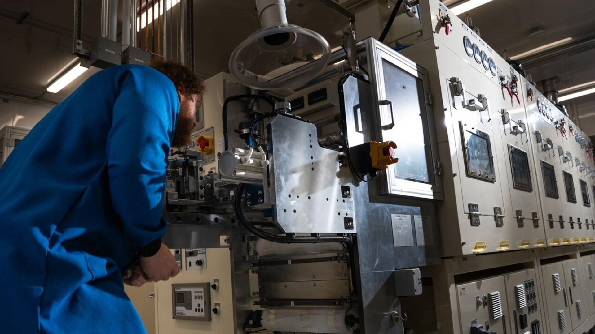
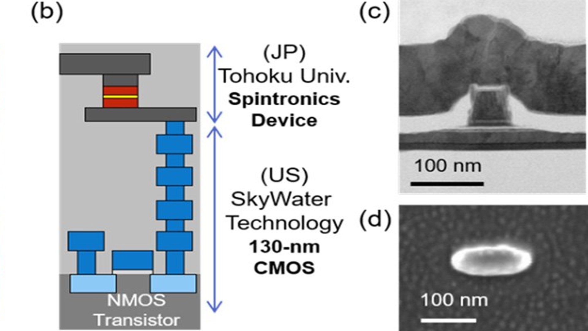
The study was led by Ju-Young Yoon, PhD, a researcher at Tohoku University’s lab for nanoelectronics and spintronics. The team integrated spintronic devices right onto a silicon chip by combining semiconductor and spintronics manufacturing techniques in both Japan and the US.

To fabricate transistors and lower interconnect layers, the team used the 130-nm (130-nanometer) CMOS process provided by SkyWater Technology, a Minnesota-based semiconductor firm. They then integrated superparamagnetic nanodevices and upper electrodes using spintronic device fabrication facilities at the university.

The resulting chip successfully demonstrated the two key characteristics required for p-bit operation. First, the team observed stochastic fluctuations in the output voltage over time, and confirmed that the device could naturally switch between different states.

They also proved that the average output could be controlled through an applied input voltage, allowing the probabilistic behavior to be tuned. The scientists said this is the first experimental demonstration of a spintronic p-bit monolithically integrated on a silicon chip using semiconductor integrated circuit processes.

The findings could enable larger spintronic p-computers. “By further advancing device and circuit technologies and increasing the number of integrated p-bits, the researchers expect spintronic p-computers to move closer to large-scale practical implementation,” the university concluded in a press release.

The study has been published in the journal IEEE Electron Device Letters.

💾

Scientists in Japan and the US have paved the way for smart computers by integrating a spintronic p-bit on a silicon chip for the first time.
  •  

US opens first national lab production line for safer grid-scale batteries

The US has recently launched a new battery production line, which is expected to help researchers develop safer and cheaper energy storage technologies for the electric grid.

The new line is housed at the Grid Storage Launchpad (GSL), a 93,000-square-foot research facility. It is run by the Department of Energy’s (DOE) Pacific Northwest National Laboratory (PNNL) in Richland, Washington State.

According to PNNL, the newly commissioned production line features a total of 16 pieces of equipment inside a 1,400-square-foot laboratory. It is reportedly the first prismatic battery cell production line at a US national laboratory.

Researchers at PNNL pointed out that it will allow them to manufacture, test, and validate advanced battery designs at an industrially relevant scale. “This helps our researchers bridge the gap between science and industry,” Adam Jivelekas, GSL operations manager, said.

A new grid storage hub

The line will produce prismatic battery cells. These are rectangular and larger than cylindrical cells, and shaped like a nine-volt battery (9V). As a result, they contain more energy per cell. Developed with a heavier metal casing, they are less prone to overheating, which makes them increasingly popular for storing energy on the electric grid.

Mark Weller, PhD, a PNNL materials scientist and the principal investigator of the project, explained that metal transfers heat more efficiently than most materials. This allows these batteries to cool more easily. “If you have better heat transport, if the cells are more mechanically uniform, if they’re packed more efficiently, all those things can translate to not just higher safety, but lower cost,” he added.

In addition, their rectangular shape means they can be stacked neatly together. This reduces wasted space compared to cylindrical alternatives. Efficient packing helps boost energy density at the pack level.

As per Jivelekas, the facility will help speed up the transition from battery research to production. “We can help external researchers or industry partners test and validate their prismatic cell designs,” he pointed out.

Start of operations

PNNL noted that the facility is located inside a specialized dry laboratory, where humidity levels are kept lower than those found in some of the driest places on the planet. Maintaining these conditions is critical, as trace levels of moisture can degrade the sensitive battery components.

The facility wrapped up testing earlier this year. The scientists are now preparing validation projects intended to demonstrate its capabilities. Well emphasized that the real test is proving it can be used to consistently manufacture high-quality prismatic cells.

“Making a coin cell takes a few milligrams of material; making a prismatic cell takes at least a kilogram,” he elaborated in a press release. “When you scale up like that, you can’t assume that a chemistry that worked well in a coin cell will work just as well in a prismatic cell.”

To demonstrate the approach, the research team will produce and evaluate two promising battery chemistries to use in prismatic cells. These include sodium-ion and lithium-iron-phosphate (LFP).

Following production, the researchers will submit these two prismatic cell types to a number of tests to evaluate their performance and safety. “With this capability, we can do the research and development and pilot-scale testing that is difficult for companies to justify and help facilitate a smoother handoff to get advanced battery concepts to market,” Weller concluded.

💾

A new battery production line in the US will test and validate advanced prismatic cells for future grid energy storage systems.
  •  
❌