❌

Reading view

COXEM Targets HBM Inspection With Atmospheric-Pressure SEM Technology
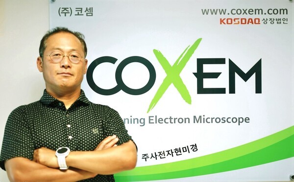
COXEM CEO Lee Jun-hee. (Photo: THE ELEC)

COXEM, a scanning electron microscope (SEM) specialist, is transforming itself into a maker of nondestructive inspection equipment for advanced semiconductor packaging. The company has begun supplying modules for high-bandwidth memory (HBM) analysis and plans to introduce automated inspection equipment for panel-level packaging (PLP) and glass substrates.

"The ion beam polisher, which precisely polishes semiconductor cross sections, was developed into equipment in collaboration with a domestic equipment company," COXEM CEO Lee Jun-hee said in a recent interview at the company's headquarters in Daejeon. "It has already been supplied to major semiconductor manufacturers and is undergoing mass-production evaluations."

COXEM, founded in 2007, is a South Korean developer and manufacturer of SEMs. The company started by licensing technology from the Korea Research Institute of Standards and Science (KRISS). It localized compact tabletop SEMs in the early 2010s and ranked fifth globally in sales in 2022, establishing its competitiveness in the market.

Lee, who holds a doctorate in electrical and electronic engineering from the Korea Advanced Institute of Science and Technology (KAIST), joined COXEM as head of its research center in 2010 and led research and development (R&D) of the technology. Lee was recognized for his technology development capabilities and business planning skills in 2012.

Ion Beam Polisher Module for HBM, MLCC Targets Qualification Early Next Year
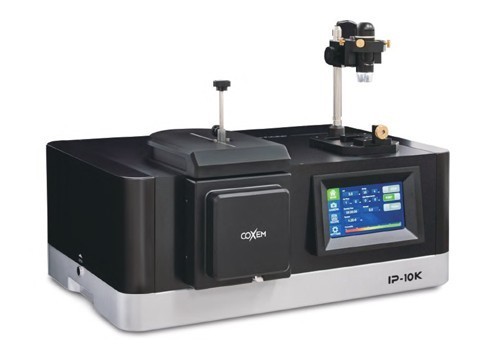
COXEM's IP-10K ion beam polisher. (Photo: COXEM)

An ion beam polisher is preprocessing equipment used to etch and polish a sample before it is examined with an electron microscope. It is based on ion miller commercialization technology that COXEM completed in 2019. COXEM's ion gun module, which emits an argon (Ar) ion beam, is installed inside the equipment. A separate SEM is also installed to observe and analyze the sample after preprocessing. AP Systems handles assembly and sales of the complete equipment.

Semiconductor analysis laboratories have traditionally polished sample cross sections manually, mainly using blades or sandpaper. The ion beam polisher automates the process. It uses a nanometer-scale particle beam to create flat cross sections without errors. It also minimizes sample damage and contamination compared with chemical mechanical polishing (CMP), preserving the sample's fine structures.

The system is similar to focused ion beam-scanning electron microscope (FIB-SEM) systems from global competitors such as Thermo Fisher Scientific and ZEISS, but differs in processing area and speed. FIB-SEM can precisely process extremely small areas of several micrometers or less and is suited to detailed analysis of nanoscale defects.

The ion beam polisher can rapidly remove material across areas as wide as several millimeters at a rate of 1,000 micrometers per hour. It can be used to inspect structures and defects including through-silicon vias (TSVs) and microbumps in HBM, as well as internal layers of multilayer ceramic capacitors (MLCCs). It is also less expensive. COXEM's CP-SEM lineup combining an ion miller and SEM costs about one-tenth as much as competing FIB-SEM systems.

"We initially guaranteed 100 hours of durability for the ion gun module, but have increased that to several thousand hours to meet the requirements of actual semiconductor mass-production lines," Lee said. "We expect to pass customer qualification tests around the end of this year or early next year and move into mass-production supply."

Nondestructive Inspection Equipment for Large Substrates Under Development
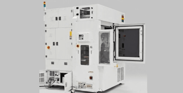
COXEM's Eirtron automated inspection equipment under development. (Photo: COXEM)

COXEM is also preparing semiconductor inspection equipment under its Eirtron brand. The equipment is designed for nondestructive observation of large-area samples, including wafers, large panels and glass substrates, during manufacturing. It is based on atmospheric-pressure scanning electron microscope (A-SEM) technology developed by COXEM.

Conventional inspection of large substrates requires cutting cross sections and moving them to an analysis laboratory. This is because conventional SEMs used for inspection rely on sealed high-vacuum chambers, limiting sample size. SEMs inspect samples by analyzing signals reflected from an irradiated electron beam. If the beam collides with air particles and scatters, the signal weakens and the detected image becomes blurred. High-vacuum chambers are used to prevent this.

A-SEM addresses this issue while maintaining high-resolution imaging with 30-nanometer resolution. This is achieved by completely separating the electron column, including the electron gun that emits the beam, from the external environment using a graphene membrane.

Graphene has high electron transmittance, allowing the beam to pass while blocking outside air. A multi-window structure allows it to withstand pressure of one atmosphere. The graphene membrane and signal detector are positioned as close as possible to the sample, while helium gas is injected to minimize electron-beam scattering and signal loss. These are all proprietary technologies patented by COXEM.

A-SEM can observe samples in ambient air at atmospheric pressure, eliminating size restrictions. It also removes the need for complex preprocessing steps such as evacuating a vacuum chamber or cutting samples, helping reduce process time.

"A-SEM technology enables real-time observation and analysis on production lines without damaging samples, making it an innovation that could shift the paradigm of semiconductor inspection processes," Lee said. "By commercializing automated A-SEM equipment, we aim to take the lead in the semiconductor equipment market currently dominated by overseas companies such as Applied Materials and Hitachi."

A test model of COXEM's automated equipment is currently undergoing validation by a major South Korean substrate company. The company plans to expand its target customer base to outsourced semiconductor assembly and test (OSAT) companies.


  •  

YMC Plans at Least 15 Billion Won in Dividends Over Three Years

Equipment components made by YMC. (Source: YMC)

YMC, a maker of components and materials for semiconductor and display equipment, plans to distribute at least 15 billion won in dividends to shareholders over three years starting this year.

YMC disclosed the shareholder value enhancement plan on Sept. 16. The company updated a plan announced in April, setting numerical targets for shareholder returns.

YMC will use 30% of net income as a source for dividends. It also set a minimum dividend level. The company plans to pay at least 5 billion won annually from this year through 2028, for a cumulative total of at least 15 billion won over the three years.

The company will also continue to cancel treasury shares. YMC canceled 500,000 treasury shares in March and plans to cancel at least another 630,569 shares by year-end, equivalent to about 50% of the 1,261,138 shares it currently holds. If completed as planned, the total number of shares outstanding will decline by at least 3.32%. Including shares canceled in February 2023, cumulative cancellations are expected to exceed 1.63 million shares.

YMC has also established a system to monitor implementation of its shareholder value enhancement plan. The company will carry out the plan under the management and supervision of its board and conduct a self-assessment at least once a year, disclosing its implementation status. It also plans to expand investor communications through domestic and overseas investor relations events and press releases.

"The shareholder value enhancement plan demonstrates our strong confidence in improving the company's future performance and our commitment to shareholder returns," YMC said. The company posted consolidated revenue of 100.5 billion won and operating profit of 3.89 billion won in the first half of 2026, up 19.2% and 55.3%, respectively, from a year earlier. A new semiconductor plant in Dangjin, South Chungcheong Province, completed last year, began full-scale mass production this year, driving revenue growth and improved profitability.

YMC manufactures and supplies diffusers and susceptors for chemical vapor deposition (CVD) equipment as well as vacuum equipment components. Diffusers uniformly distribute gas inside process equipment chambers to help form even thin films on treated surfaces or facilitate etching. Susceptors support wafers or substrates to maintain uniform temperatures during thin-film deposition.

  •  

Samsung Electronics to Expand DDR5 Module Output Only Through Outsourcing

Samsung Electronics is expanding production capacity for DDR5 memory modules and SSDs exclusively through outsourcing. (Photo: Samsung Electronics)

Samsung Electronics plans to outsource all additional production of conventional memory modules as it focuses its in-house capacity on high-value memory products such as high-bandwidth memory (HBM).

Samsung Electronics is strongly urging outsourced semiconductor assembly and test (OSAT) partners to expand production lines to meet growing demand for conventional memory modules, according to industry sources on Sept. 15. Instead of expanding its own production capacity for DDR5 memory modules and solid-state drives (SSDs) used in PCs, servers and laptops, the company is increasing allocations to outsourcing partners.

β€œSamsung Electronics lacks space to expand existing back-end production lines needed to manufacture semiconductors for artificial intelligence (AI), so it is reallocating space and equipment at packaging plants in Cheonan and Onyang to advanced packaging lines, including HBM,” a person familiar with the matter said. β€œThe company has decided to handle most increases in conventional memory module production through outsourcing rather than expanding its own capacity.”

Another person familiar with the matter said, β€œSamsung Electronics has asked its partners since June last year to increase investment in production lines for conventional DDR5 memory modules and SSDs. This year, it has even proposed that partners bring forward capacity expansions from their existing plans.”

Samsung Electronics is expanding outsourcing of conventional modules because it needs to use its limited production facilities more efficiently. The company plans to begin construction this month of a new 6 trillion won HBM plant at its Onyang campus, but completion will take several years.

A new $1.5 billion back-end processing plant under construction in an industrial park in Thai Nguyen Province in northern Vietnam will also be dedicated to testing older memory products, including DDR4, low-power LPDDR4, NAND flash and universal flash storage (UFS) products. That leaves Samsung Electronics with limited in-house facilities available to increase conventional module production.

DDR5 memory modules are assembled by mounting prepackaged DRAM and NAND chips and passive components onto printed circuit boards (PCBs) using surface-mount technology (SMT). The process is relatively less complex than advanced packaging for products such as HBM, allowing outsourcing partners to expand production capacity sufficiently.

Hanyang Digitech, SFA Semicon and Dreamtech Expand Facilities

Memory modules. (Photo: Hanyang Digitech)

Samsung Electronics’ outsourcing partners are also expanding production facilities in line with the company’s increased outsourcing of memory modules.

Dreamtech, which began mass production of DDR5 modules in India in November last year, is also expanding its production lines. In June, the company approved equipment investment to convert and expand its Noida Plant 1 in India, which had assembled printed board assemblies (PBAs) for smartphones, into a large-scale memory module production line. The expansion work will be completed this month, followed by a gradual increase in production capacity. The plant is ultimately expected to secure annual production capacity of more than 50 million units.

Hanyang Digitech is working to improve productivity at its existing memory module plant in Vietnam. The company invested more than 31.5 billion won in the first half of this year to introduce new machinery and automate production processes.

SFA Semicon is transferring DDR5 testing and module assembly equipment previously used at Samsung Electronics’ Onyang campus to SFA Semicon’s plant in the Philippines. The first phase is scheduled to begin operations in November, followed by the second phase in the second quarter of next year. The move is expected to significantly increase DDR5 final testing and module production capacity. SFA Semicon handles fine-pitch ball grid array (FBGA) packaging of memory chips at its Cheonan plant in South Chungcheong Province and conducts final testing and module assembly at its Philippine plant.

  •  
❌