❌

Reading view

Siemens EDA Says AI Can Cut Chip Design Time by Up to 10x
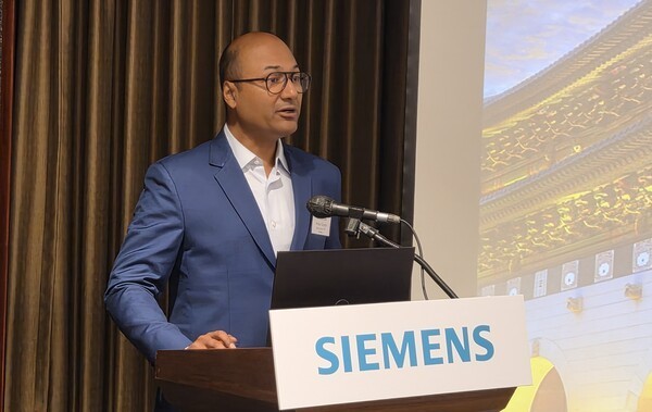
Ankur Gupta, Senior Vice President of IC Products at Siemens Digital Industries Software's Electronic Design Automation (EDA) business, introduces the company's AI strategy during a media briefing held at Lotte Hotel World in Seoul on Aug. 11. (Photo: THE ELEC)

Siemens EDA outlined how artificial intelligence (AI) can reduce semiconductor design time by as much as tenfold, highlighting multi-agent AI as a key technology for addressing the growing complexity of chip development.

Ankur Gupta, Senior Vice President of IC Products at Siemens Digital Industries Software's Electronic Design Automation (EDA) business, presented the company's AI-native design strategy during a media briefing held at Lotte Hotel World in Seoul on Aug. 11.

"Last month, we integrated a broad range of agentic AI capabilities into our EDA platform, including multi-agent workflows, self-verification and long-duration autonomous execution," Gupta said.

Multi-agent AI enables multiple AI agents to divide and coordinate semiconductor design tasks. After engineers specify design parameters such as manufacturing process, voltage and temperature conditions, the agents automatically perform verification, debugging and design modifications. Siemens introduced its AI-powered EDA system, Fuse, in 2025.

According to the company, multi-agent AI can accelerate transistor characterization workloads by up to ten times while reducing token costs by roughly 90%.

"Engineers at large companies are restricting or even suspending the use of large language models because token budgets have become unsustainably high," Gupta said. "The EDA industry recognizes this as a critical challenge and is developing technologies that deliver much higher token efficiency."

Siemens is also collaborating with Nvidia to develop AI-enabled EDA tools. Earlier this year, the two companies announced a strategic AI partnership aimed at integrating AI throughout the semiconductor design flowβ€”from register-transfer level (RTL) design through verification. Under the collaboration, Nvidia's AI infrastructure and Nemotron models will be incorporated into Siemens' EDA software.

Gupta said modern semiconductor designs are reaching unprecedented levels of complexity.

"Today's chips contain more than 200 billion transistors and exceed thermal densities of 100 watts per square centimeter," he said. "Conventional design approaches can no longer keep pace with the speed of the market."

He added that even modest improvements in chip efficiency can have a substantial impact.

"A 5% reduction in power consumption translates into significant energy savings at the system level, making it an important factor in building a more sustainable industry," he said.

Other leading EDA vendors, including Synopsys and Cadence Design Systems, are also incorporating AI capabilities into their design platforms.

Gupta said Siemens differentiates itself through its focus on design verification, emphasizing that the company provides a comprehensive integrity platform.

"In semiconductor design, a single minor error can result in design failure or lower manufacturing yields," he said. "Because such failures can cost hundreds of millions of dollars, building software that customers can trust is the industry's highest priority."

Siemens also said AI can significantly reduce verification time, one of the most time-consuming stages of semiconductor development. According to the company, its EDA tools can accelerate automatic test pattern generation (ATPG) simulation by up to five times for certain workloads. ATPG simulation is used to validate test patterns in virtual environments before they are applied to detect manufacturing defects in semiconductor devices.

  •  

Fadu Launches Recruitment Drive for System Semiconductor Engineers

Fadu headquarters in Seoul's Gangnam district. (Photo: THE ELEC)

South Korean semiconductor company Fadu announced on Aug. 10 that it is recruiting junior-level engineers, ranging from new graduates to professionals with up to eight years of experience.

The company will accept applications through Aug. 23 as part of an effort to secure top talent and strengthen its future technology competitiveness.

Applicants will undergo a coding test later this month, followed by interviews in September. Successful candidates are expected to join the company in November and work at Fadu's headquarters in Seoul's Gangnam district.

The recruitment program is expected to hire more than a dozen employees. Eligible candidates include bachelor's degree graduates as well as engineers with up to eight years of experience in hardware or embedded software development.

Open positions include firmware development, firmware verification and test engineering roles.

The selected employees will analyze customer requirements for Fadu's enterprise solid-state drive (eSSD) products and help incorporate those requirements into product development. Responsibilities will also include analyzing eSSD test results, identifying root causes of issues and proposing improvements.

  •  

Iron Device Surpasses 100 Million Units in Cumulative Smart Power Amplifier Shipments

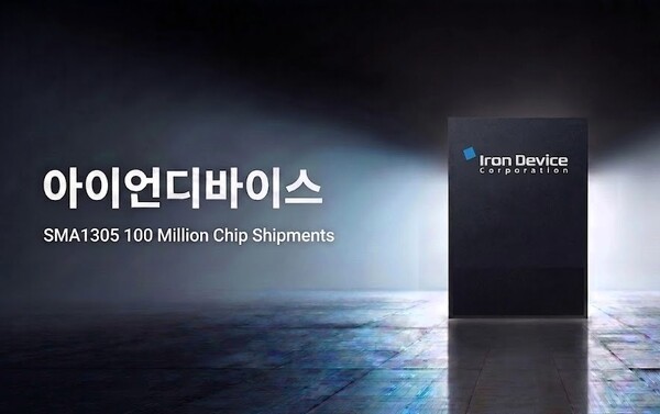
Β (Source: Iron Device)

Iron Device said on Aug. 10 that cumulative sales of its SMA1305 smart power amplifier for Samsung Electronics mobile devices and tablets have exceeded 100 million units, reaching the milestone four years after shipments began.

The company began supplying the SMA1305 in January 2022. According to its latest tally, cumulative shipments surpassed 100 million units as of March this year, equivalent to an average of approximately 25 million units supplied annually.

On average, two SMA1305 chips are installed in each mobile device, while tablets typically use four units per device.

"The achievement demonstrates that our technology is being recognized in the global market," said Lee Young-taek, a director at Iron Device. "We also have high expectations for sales of follow-up products."

The SMA1305 is a mixed-signal semiconductor used in smartphones and tablets. The chip amplifies audio signals to drive speakers and incorporates Iron Device's proprietary speaker protection algorithm, which the company says improves performance and reliability compared with competing products. The device also integrates low-noise, low-power design and audio signal processing technologies to maximize system efficiency.

Iron Device develops chips that combine analog, digital and power technologies on a single device. The company has recently expanded into the on-device AI market, targeting applications in smart glasses and humanoid robots.

"Audio products are evolving beyond simple sound input and output devices into AI sensors capable of understanding their surroundings," the company said. "We define audio as a core interface for interacting with the real world and are developing technologies accordingly."

  •  

LX Semicon Begins Supplying Automotive MCUs to Hyundai Motor and Kia

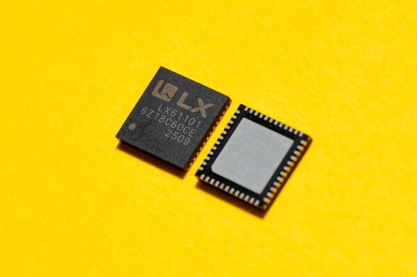
LX Semicon's LX61101 microcontroller unit (MCU). (Photo: LX Semicon)

LX Semicon has begun supplying automotive semiconductors to Hyundai Motor and Kia, marking the first major achievement from a new business initiative launched four years ago to diversify beyond display driver ICs (DDIs).

The company said on Aug. 10 that it has been supplying its automotive microcontroller unit (MCU), code-named LX61101, to Hyundai Motor and Kia vehicles since July. The chip has already been installed in vehicles produced from July, and the scope of adoption is expected to expand. Specific vehicle models and shipment volumes were not disclosed due to non-disclosure agreements (NDAs) with customers.

The LX61101 is a motor-control-focused MCU based on a 40 MHz Arm Cortex-M3 core. It is optimized for motor control in automotive body electronics systems. When installed in vehicle doors, the chip monitors and controls motor speed, position and rotation direction in real time. For example, if an obstacle is detected while an automatic door is closing, the system can reverse operation and reopen the door.

LX Semicon said South Korean companies were involved across the entire process, including foundry manufacturing and back-end supply chain management (SCM).

The company has been developing automotive MCUs as a future growth engine since 2022. In 2023, it participated in Hyundai Motor and Kia's supplier selection process for new business projects. Following three years of development and testing, LX Semicon has now entered mass production of the LX61101.

The chip also meets key automotive semiconductor standards, including the AEC-Q100 reliability qualification standard and ISO 26262 functional safety requirements.

  •  
❌