Lotte Energy Materials has entered the market for ultra-thin copper foil used in artificial intelligence (AI) data centers and is considering a third capacity expansion based on binding customer agreements.
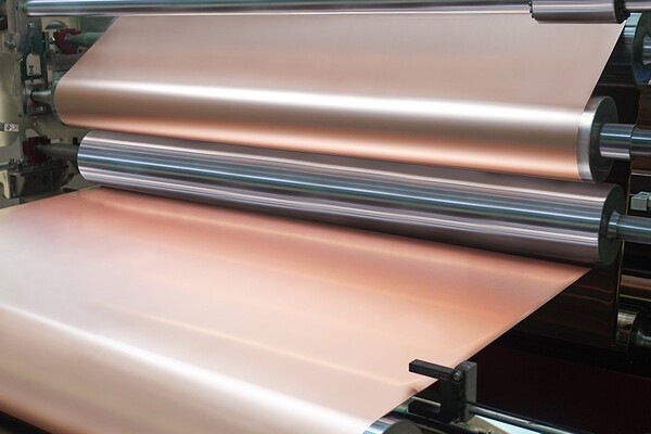
The company disclosed its third-phase expansion strategy on Aug. 6, centered on ultra-thin copper foil products. Ultra-thin copper foil, measuring between 1 and 3 micrometers in thickness, is a next-generation circuit material used in AI data center optical transceivers and semiconductor packaging applications. The product is significantly more difficult to manufacture than conventional circuit foil due to its extremely thin profile.
Lotte Energy Materials currently supplies reverse-treated foil (RTF) and high-voltage low-profile (HVLP) copper foil for AI data center optical transceivers. The materials are used in the inner and outer layers of transceiver substrates. RTF products range from 12 to 70 micrometers in thickness, while HVLP products range from 12 to 35 micrometers.
The company plans to expand its portfolio into the thinner ultra-thin copper foil segment to target the rapidly growing optical transceiver market.
The ultra-thin copper foil market is currently dominated by Japan’s Mitsui Chemicals. However, rising investment in AI data centers has created an opportunity for new entrants. Demand for ultra-thin copper foil has surged as optical networking transitions toward 800G and 1.6T architectures. At the same time, North American customers have increasingly sought non-Chinese supply chains. Lotte Energy Materials is currently the only company operating a circuit foil production base in South Korea.
The company emphasized that any third-phase expansion will depend on securing binding agreements with customers. Future investment decisions will be based on confirmed demand commitments rather than speculative capacity additions.
“Customer demand for additional expansion is strong, and we are reviewing a third expansion phase either at available space within our domestic facilities or at a new site,” the company said. “The project will proceed once binding customer contracts are signed and economic feasibility is secured.”
Lotte Energy Materials added that it plans to determine the timing and scale of investment through discussions with customers and is already conducting preliminary preparations, including concept design work, due to strong demand from key clients.
The broader circuit foil business is also shifting toward AI-related applications. Demand has expanded beyond traditional IT products into high-end copper foil for AI accelerators, network switches and optical transceivers.
High-value-added HVLP products currently account for roughly 20% of circuit foil sales. Following completion of the second expansion phase next year, the proportion is expected to exceed 50%. Some production lines dedicated to AI-focused HVLP products are already being operated exclusively for specific customers.
The company began mass production earlier this year of HVLP 1 and HVLP 2 products used in AI networking equipment supplied to Nvidia systems. Production yields have reached approximately 60%, and commercial shipments began in the second quarter after customer qualification procedures were completed.
Production capacity for HVLP 3 and HVLP 4 products designed for Nvidia’s next-generation Rubin platform was secured through the first expansion phase completed in May. Initial mass production began in the second quarter, and related revenue is expected to increase in the second half as Rubin shipments expand.
Lotte Energy Materials completed its first expansion phase in May, increasing annual circuit foil production capacity from 3,700 metric tons to 6,700 metric tons.
The second expansion phase, currently under construction, will add annual capacity of 16,000 metric tons. Major equipment contracts have been finalized and manufacturing has begun. The company plans to accelerate equipment delivery schedules and start operating part of the new production lines in the second quarter of 2027, ahead of the original timetable, with full operations beginning in the fourth quarter.
The company also reported second-quarter consolidated revenue of 286.4 billion won and an operating loss of 9.2 billion won. Despite higher copper foil sales volumes and increased revenue from AI-focused high-end products, earnings remained in the red due to initial expansion costs and production stabilization expenses.
“Both pricing and demand are entering a more stable phase,” Chief Executive Officer Kim Yeon-seop said. “We believe a turnaround is only a matter of time and can be achieved in the near future.”
Chinese display maker Visionox is preparing a follow-on investment for its 8.6-generation OLED production line, with industry attention focused on whether South Korean equipment suppliers such as YAS can secure orders after missing out on the first phase.
According to industry sources on Aug. 6, Visionox is planning a second-phase investment for its V5 fab under construction in Hefei, Anhui Province. While the exact timing has not been finalized, the project is widely expected to begin in the first quarter of 2027.
The V5 facility is designed for a total production capacity of 32,000 glass substrates per month. The first phase covers 8,000 substrates per month, while the second phase will add the remaining 24,000 substrates per month—three times the size of the initial investment.
The first phase included equipment supplied by South Korean companies such as AP Systems, SynusTech and ICD. Applied Materials (AMAT) won the order for the deposition equipment, widely considered the most critical tool in the production line. The company began delivering equipment in May and is currently conducting installation, commissioning and process validation for Visionox's ViP technology, a fine-metal-mask (FMM)-less OLED manufacturing process. Yield rates on the line are reportedly in the 30–40% range.
Although both AMAT and YAS deposit organic materials onto substrates by heating solid organic emissive materials in a vacuum environment, their approaches differ significantly.
AMAT uses a vertical deposition architecture in which 8.6-generation glass substrates are positioned upright during processing. The system integrates deposition, substrate transfer and encapsulation processes within a connected vacuum environment. Maintaining uniform film thickness across large vertically transported substrates is a key technical challenge.
YAS, by contrast, employs a horizontal architecture in which substrates remain flat while organic materials are deposited from evaporation sources located beneath them. The system maintains a constant distance between the evaporation source and substrate to ensure uniform film formation across the entire panel. As a result, chamber structures, transfer systems and overall equipment configurations differ substantially from those used by AMAT.
AMAT benefits from operational data and process conditions accumulated from the first-phase V5 line. If Visionox selects the same equipment for the expansion, previously developed deposition recipes and process parameters can be reused. Adopting YAS equipment, however, would require fresh validation of both equipment performance and manufacturing processes because of the different substrate-handling architecture.
Commenting on the possibility of YAS participating in the second phase, a Visionox official said, "We are currently validating the AMAT equipment, but yields remain low and pricing is high. If we adopt YAS equipment, we would need to conduct new verification work, so there are many factors to consider."
Visionox had also previously considered applying the conventional FMM process to portions of the V5 line. In May last year, the company discussed introducing FMM deposition equipment from Japan's Canon Tokki and South Korea's Sunic System. However, it ultimately chose the ViP approach.
According to Visionox, the likelihood of reverting to FMM technology in the second phase remains low.
Asked whether poor yields on the initial ViP line could lead the company to reconsider FMM technology, a Visionox official said, "Even if yields do not meet expectations, there is almost no possibility of returning to the FMM method. If we were to go back to FMM, it would raise questions about the rationale behind the investment, and we do not know whether the Hefei government would approve such a move."
Visionox is expected to determine the supplier for the second-phase deposition equipment based on the results of equipment installation, commissioning and ViP process validation on the first production line.
For the first-phase investment, Visionox selected lithography equipment from Canon, excimer laser annealing (ELA) and laser lift-off (LLO) systems from AP Systems, plasma-enhanced chemical vapor deposition (PECVD) and sputtering equipment from Applied Materials, and certain sputtering tools from ULVAC. Dry etching equipment was supplied by Tokyo Electron and ICD, while logistics and material-handling systems for array and deposition processes were provided by SynusTech.
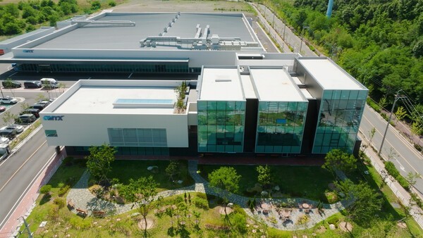
CMTX’s M Campus in Gumi, North Gyeongsang Province (Photo: CMTX)
CMTX’s M Campus in Gumi, North Gyeongsang Province (Photo: CMTX)
CMTX said through its shareholder communication platform that it has no plans to issue convertible bonds (CBs) or bonds with warrants (BWs), dismissing concerns raised after its recent extraordinary general meeting.
The company said amendments approved at the extraordinary shareholders’ meeting held on July 22 included the introduction of an independent director system in line with revisions to Korea’s Commercial Act, as well as an increase in the issuance limits for CBs and BWs. “We currently have no plans to issue CBs or BWs,” CMTX said.
Following shareholder approval, CMTX increased the issuance limit for both CBs and BWs to 50 billion won each from 10 billion won previously. The company said the move was intended as a preparatory measure to provide flexibility for future mergers and acquisitions (M&A) and strategic investment opportunities. It added that it currently holds approximately 90 billion won in cash and cash equivalents and has secured 100 billion won in available credit facilities from financial institutions, making external fundraising unnecessary at this time.
CMTX said that if it had been planning a large-scale issuance of CBs or BWs in the near future, it would have raised the limits by a substantially larger amount. The company described the amendments as a minimum-level revision designed to address potential future needs. It also emphasized that any future financing decisions would be made with the goal of minimizing dilution for existing shareholders.
The company also revised its articles of incorporation to reflect changes to the Commercial Act, including replacing outside directors with independent directors and increasing the required proportion of independent directors from at least one-quarter of the board to at least one-third.
Through its recently launched shareholder communication forum, CMTX said it plans to continue sharing key management information, including earnings analysis, investment and capacity expansion progress, new customer acquisition, and shareholder return policies.
HanWool Semiconductor on Aug. 6 unveiled its strategy for AI-based multilayer ceramic capacitor (MLCC) back-end manufacturing equipment, highlighting an ultrasound inspection system and a second-generation mounter capable of conducting high-speed, full-scale inspection of internal defects.
The company aims to expand its presence in automotive electronics and AI server markets by transforming MLCC inspection methods. As demand grows for high-reliability MLCCs, inspection requirements are extending beyond external appearance to internal structures and evolving from sample-based checks to high-speed, 100% inspection.
HanWool is developing an “AI-based ultrasound full inspection system” capable of non-destructively detecting microscopic cracks, delamination and voids inside MLCCs. The system combines AI-driven judgment technology with ultrasound signal analysis to overcome the limitations of conventional sample inspections while improving both inspection speed and reliability.
A key element of the strategy is the company’s proprietary deep-learning inspection platform, HaWAIe. The platform is designed to detect defects such as microcracks, chipping, electrode failures and foreign materials that are difficult to identify through visual inspection or rule-based algorithms. HanWool plans to expand its use beyond visual inspection equipment to ultrasound inspection systems and process automation equipment.
The company is also developing a second-generation mounter designed for high-value-added MLCC production. HanWool said the new system will improve production yield and throughput by more than 30% compared with existing equipment while supporting ultra-small MLCC products.
“The MLCC inspection market is rapidly evolving from simple visual inspection toward high-speed full inspection capable of identifying internal defects,” a HanWool Semiconductor official said. “Through commercialization of our AI ultrasound inspection system and second-generation mounter, we aim to secure a leading position in the market for high-value MLCC manufacturing equipment.”
Simmtech reported a sharp increase in second-quarter earnings as sales of package substrates for artificial intelligence semiconductors continued to expand.
The company disclosed on Aug. 5 that it recorded consolidated revenue of 514.6 billion won and operating profit of 62.9 billion won for the second quarter.
Compared with the same period last year, revenue increased 51.0% while operating profit surged 1,034.4%, more than elevenfold. On a sequential basis, revenue rose 21.8% and operating profit increased 358.7%.
For the first half of 2026, Simmtech posted cumulative revenue of 936.9 billion won and operating profit of 76.6 billion won.
The company's operating margin reached 12.2% in the second quarter, up 10.6 percentage points from a year earlier and 9.0 percentage points from the previous quarter.
Net profit totaled 44.9 billion won, compared with a net loss in the year-earlier period, marking a return to profitability.
Simmtech expects growth to continue in the second half of the year.
In a separate disclosure, the company forecast second-half consolidated revenue of 1.0719 trillion won and operating profit of 163.1 billion won. The projected operating profit exceeds the company's first-half operating profit by more than two times.
The company said demand for system IC package substrates is expected to remain strong, while sales of products for SOCAMM are set to expand in earnest.
As a result, the proportion of high-value-added products used in AI applications is expected to increase further during the second half of the year.
Taiwan-based GlobalWafers has formally acknowledged growing supply shortages in the silicon wafer market, signaling a potential shift toward higher wafer prices as demand from artificial intelligence and advanced semiconductor applications accelerates.
During its second-quarter earnings conference call on Aug. 4, GlobalWafers said supply-demand imbalances are already emerging across the semiconductor wafer industry.
"The supply-demand imbalance in the wafer industry is already underway," the company said. "Our 12-inch (300mm), 8-inch (200mm) and 6-inch (150mm) production lines are effectively operating at full utilization, and supply constraints have already appeared for certain advanced 12-inch products."
The company attributed the tightening market to rapidly growing demand from AI semiconductors, high-bandwidth memory (HBM), silicon photonics and advanced packaging technologies.
GlobalWafers said both memory and logic chip manufacturers are increasingly seeking to secure long-term production capacity, turning potential shortages into a reality.
Similar trends are emerging across the broader wafer industry.
German wafer supplier Siltronic said during its earnings announcement on July 30 that inventory levels at memory and logic customers have normalized and customers have begun rebuilding safety stock inventories.
The company added that inventory replenishment is expected to further increase wafer demand and that requests for 300mm wafers are coming not only from existing customers but also from new ones.
Industry leader Shin-Etsu Chemical reported on July 24 that shipments of 300mm wafers increased by double-digit percentages both year over year and sequentially.
Japanese wafer manufacturer SUMCO also indicated in May that customer inventory adjustments were approaching completion.
South Korea's SK Siltron has been expanding production capacity through the phased startup of new facilities, but industry sources said demand growth is outpacing those additions.
The structure of long-term agreements (LTAs) is also changing.
Historically, LTAs were primarily designed to ensure stable wafer supplies for customers. Increasingly, however, they are being used as tools to secure future manufacturing capacity in anticipation of supply shortages.
Contract durations are also lengthening, with agreements increasingly extending from the traditional three-year range to five to eight years.
Last month, GlobalWafers signed a 10-year LTA with Micron, one of the longest agreements in the wafer industry's history. The contract, which begins next year, includes strategic financial support in the form of upfront payments.
The company said most of its revenue in the second half of this year and the first half of next year is expected to come from LTAs.
Shin-Etsu Chemical has stated that all of its 300mm wafer shipments are currently supplied under LTAs. Siltronic said roughly two-thirds of its shipments are sold through similar agreements.
Some memory customers are already requesting supply allocations for two to three years into the future.
Signs of pricing pressure are also emerging.
As supply tightens, prices in the spot market have started rising ahead of contract prices.
Siltronic said prices for non-LTA 300mm wafers have begun increasing, while GlobalWafers expects spot prices in the second half of 2026 to be higher than in the first half.
The industry expects price increases to eventually spread to long-term contracts as well.
GlobalWafers said it is discussing price increases with customers to reflect higher costs for raw materials, energy, logistics and labor.
"Existing LTAs will maintain their contracted prices, but future agreements will incorporate pricing mechanisms that reflect market conditions, product mix changes and industry developments," the company said.
Siltronic echoed the view, stating that prices must recover to levels that justify reinvestment as some LTAs come up for renegotiation in 2027 and 2028.
"We need broad and meaningful price increases," the company said.
The wafer industry has spent the past two years coping with shipment declines and pricing pressure after customer inventories surged beginning in 2023.
That trend began to reverse in late 2025 as inventories of 300mm wafers declined and inventory coverage levels fell further during the first quarter of this year, signaling the end of the industry's inventory correction cycle.
Many suppliers now view the second quarter of 2026 as the beginning of a new upcycle.
Industry participants expect supply shortages and price increases to become more pronounced from the second half of 2027.
Current shipment growth is being supported by higher utilization rates at existing semiconductor fabs. However, once new memory facilities being built by Samsung Electronics, SK hynix and Micron begin production, wafer demand could roughly double from current levels.
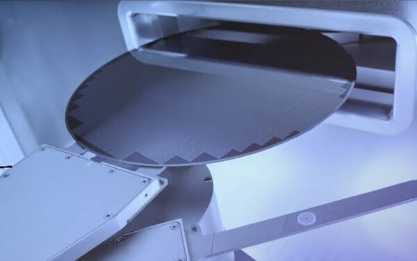
iVisionWorks is developing a semiconductor wafer inspection system. (Photo: KLA)
iVisionWorks is developing a semiconductor wafer inspection system. (Photo: KLA)
Machine vision inspection system company iVisionWorks has begun developing semiconductor wafer inspection equipment, the company announced on Aug. 5.
The new system will be a wafer metrology and inspection platform built on a high-sensitivity optical architecture. The market is currently dominated by overseas suppliers such as KLA and Hitachi High-Tech. iVisionWorks said it aims to develop a product that can compete on both defect detection capability and inspection speed.
The company plans to complete proof-of-concept (PoC) testing in the second half of this year and finish a prototype in the first half of next year. The prototype will then be used for customer evaluations.
Wafer inspection systems are used to identify defects generated during semiconductor manufacturing processes. Their performance has a significant impact on production yield and manufacturing efficiency.
Demand for wafer inspection equipment has been rising rapidly as the global expansion of artificial intelligence drives increased semiconductor production.
According to market research firm Fortune Business Insights, the global semiconductor defect inspection equipment market was valued at approximately $6.14 billion in 2025 and is projected to reach about $13.41 billion by 2034.
"We are concentrating our company-wide capabilities on entering the semiconductor inspection equipment market," said Gil Gi-jae, Chief Executive Officer of iVisionWorks.
"The semiconductor inspection equipment market has high technological barriers to entry, but we intend to leverage our accumulated precision optical technologies to establish a position in the sector and secure a new growth momentum," he added.
iVisionWorks currently supplies machine vision inspection equipment for secondary battery manufacturing processes.
Machine vision systems are automated measurement and identification platforms that combine optical hardware, software and image-processing technologies to inspect products and manufacturing processes.

 Login