
❌

Reading view

US startup to build magnetic mirror fusion research facility in Wisconsin
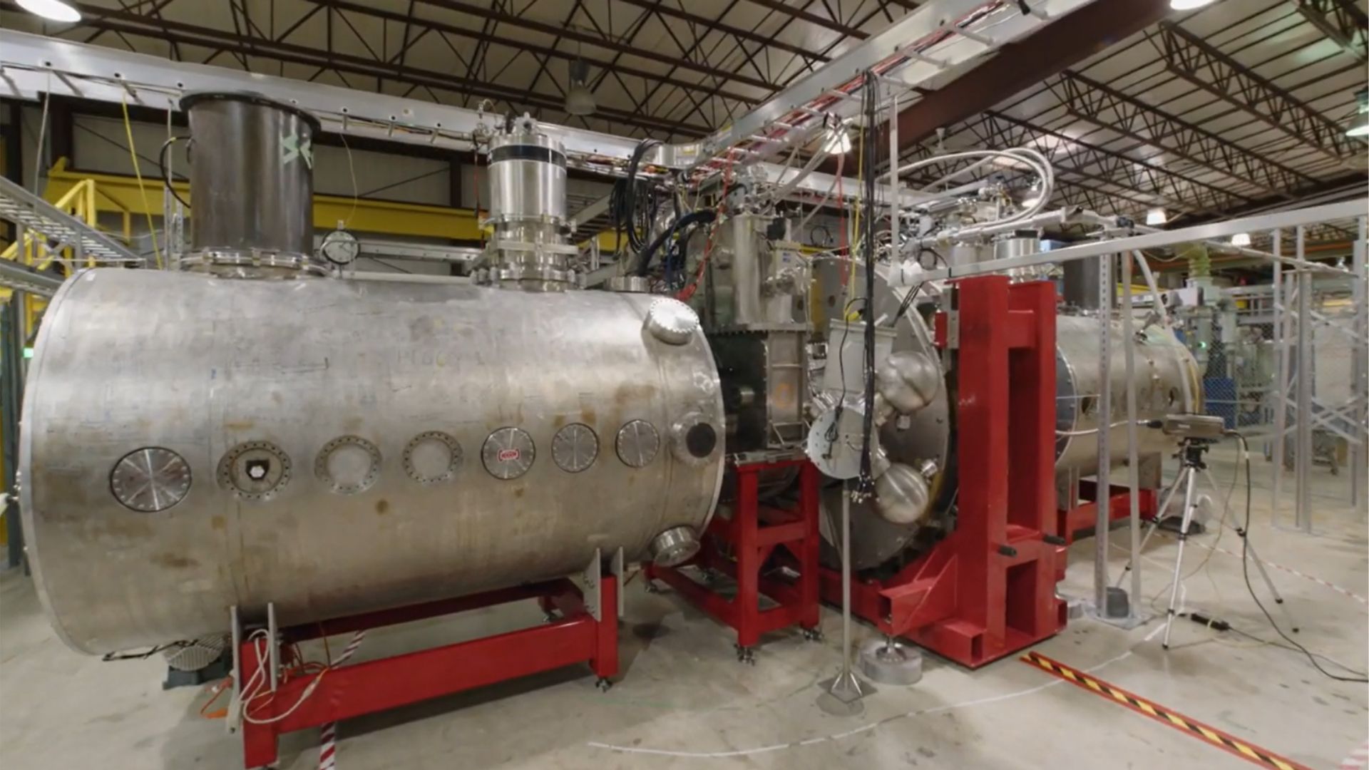
Wisconsin has committed up to $55 million in incentives to help Realta Fusion build its new headquarters and fusion research facility in Madison, a move aimed at strengthening the state’s position in the emerging fusion energy industry.

The funding package will support development of β€œThe Realta Forge” at OM Station, the site of the former Oscar Mayer plant. Realta plans to build its prototype magnetic mirror fusion machine, called Hammir, at the facility and expects to create more than 600 technical and non-technical jobs.

According to the company, the incentive package includes about $37.5 million in state sales and use tax exemptions, up to $15 million in performance-based enterprise zone tax credits from the Wisconsin Economic Development Corporation, and $2.8 million in tax increment financing from the City of Madison.

Realta said it evaluated sites in Illinois, New Jersey, New Mexico, Tennessee, and other states before deciding to keep the project in Wisconsin, where it was founded.

State backs fusion

The company expects to break ground on the facility before the end of the year. Once completed, The Realta Forge will serve as Realta’s headquarters and dedicated research and development center for advancing its compact magnetic mirror fusion technology.

β€œWe spent the better part of the past two years searching across the country to find the most favorable business environment and the most attractive site to build our R&D facility, and we found it in our own backyard,” said Realta CEO Kieran Furlong.

The company says its CoSMo fusion systems are based on the magnetic mirror concept, which uses magnetic fields to confine high-temperature plasma. Unlike conventional power plants, fusion aims to generate electricity by fusing light atomic nuclei, producing large amounts of energy without carbon emissions during operation.

Realta added that the Hammir prototype will help demonstrate the company’s fusion approach before commercial deployment.

β€œIn terms of cash today, avoided costs tomorrow, and accelerating progress, this is the most impactful state-supported fusion deal ever done in the United States,” said Realta VP of Technical Development Dominick Bindl.

Building regional hub

The announcement follows Wisconsin’s passage of Act 165 earlier this year, becoming the first standalone state law in the United States to exempt capital expenditures on fusion energy projects from state sales tax. State officials say the legislation is intended to attract companies developing next-generation energy technologies.

β€œFusion energy is not only good for our planet and our power grid, but it plays to all of our strengths as a state with our world-class research universities, research laboratories, and an incredible manufacturing and supply chain network supported by our dedicated and highly skilled workforce,” said Wisconsin Governor Tony Evers.

Madison also approved $2.8 million in tax increment financing tied to job creation at the OM Station redevelopment. According to the company, it is the city’s first tax increment financing package for private-sector job creation in a decade.

With construction expected to begin later this year, Realta said the facility will become the center for development of its magnetic mirror fusion technology while helping establish Wisconsin as a growing hub for fusion research, advanced manufacturing and high-skilled engineering jobs.
  •  

Intel ships first commercial processors made with next-generation lithography tools

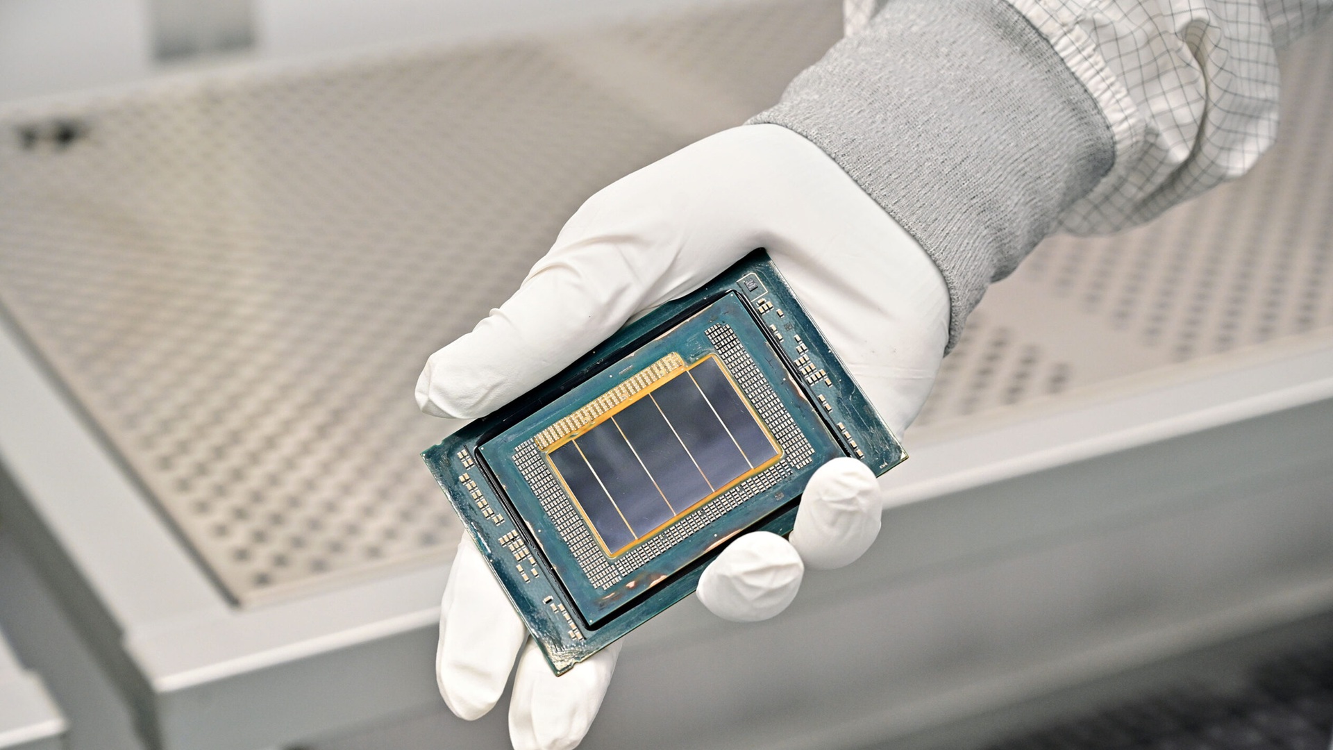
Intel Foundry has become the first chipmaker to manufacture and ship a high-volume logic product using ASML’s High NA extreme ultraviolet (EUV) lithography, marking a major step toward commercial adoption of the next generation of chipmaking technology.

The milestone applies to a subset of Intel Core Ultra Series 3 processors, code-named Panther Lake, built on the company’s Intel 18A process node. Intel said specific Intel 18A layers are now dual-qualified on ASML’s High NA EUV platform at its Oregon facility, with products shipping to customers at yields matched to the existing NXE platform.

The announcement signals a shift for High NA EUV from research and early testing into production manufacturing. Intel and ASML said the technology is being used on selected chip layers to collect manufacturing data and further optimize system setup, uptime, and production implementation before wider deployment in future process nodes.

High NA EUV is the next evolution of EUV lithography, offering higher resolution and improved process control for patterning increasingly smaller chip features. The technology is expected to help semiconductor manufacturers build denser and more complex chips while supporting future advances in computing and artificial intelligence.

Production milestone reached

ASML said the deployment builds on decades of collaboration with Intel to advance semiconductor manufacturing. The latest production milestone follows Intel’s installation of the industry’s first commercial High NA EUV system at its Hillsboro, Oregon, research and development site in 2024. The company later became the first to install and qualify ASML’s second-generation TWINSCAN EXE:5200B system, which delivers higher throughput, improved overlay accuracy, and an upgraded light source.

The Panther Lake processors are manufactured on Intel 18A, with High NA EUV used to pattern selected layers of the chips. Intel said the approach provides manufacturing experience while maintaining production performance on existing platforms.

β€œWith increased resolution and better process control, the introduction of High NA EUV marks a substantial development in semiconductor lithography,” said Christophe Fouquet, ASML President and CEO. β€œWe are proud to play a role in enabling the smaller, denser patterning that will accelerate advancements in AI and other emerging technologies.”

The companies said insights gained from production will help refine system setup, uptime and manufacturing processes, paving the way for broader adoption of the technology in future generations of semiconductor manufacturing.

Scaling future nodes

Intel described the milestone as an important step in integrating High NA EUV into commercial chip production at scale while maintaining manufacturing flexibility for future process technologies.

β€œThis milestone reflects the close technical collaboration between Intel and ASML and shows how High NA EUV can be integrated into advanced semiconductor manufacturing at scale,” said Naga Chandrasekaran, Executive Vice President and General Manager of Intel Foundry.

According to Intel, qualifying High NA EUV on selected Intel 18A product layers allows the company to continue delivering production output while evaluating how the technology can support future process nodes with higher performance, greater transistor density, and improved manufacturing flexibility.

With Panther Lake now entering high-volume manufacturing using High NA EUV, Intel becomes the first company to ship commercial high-volume logic products built with the technology, providing an early demonstration of how next-generation lithography can move from development into large-scale chip production.

  •  
❌