
❌

Reading view

Dodge Charger maker road-tests solid-state EV battery hitting 90% charge in 18 minutes

Stellantis has integrated Factorial Energy’s solid-state battery cells into a Dodge Charger Daytona development vehicle and begun road testing the technology, marking a key step toward bringing solid-state batteries into production vehicles.

The milestone is the first time Factorial’s FEST (Factorial Electrolyte System Technology) solid-state cells have been installed in a Stellantis vehicle. The companies will now evaluate battery performance, reliability, and safety under real-world driving and charging conditions.

The development follows laboratory validation completed in 2025, when Stellantis and Factorial demonstrated automotive-scale FEST cells with an energy density of 375 Wh/kg. The cells also achieved charging from 15 percent to 90 percent in 18 minutes and operated across temperatures ranging from -22 °F to 113 °F.

Moving from laboratory testing to an on-road vehicle required engineers to redesign parts of the battery system. Stellantis said it developed a patented mechanical architecture that allows the solid-state cells to fit within an existing battery pack while maximizing performance.

From lab to road

Engineers also modified battery controls and pack design to meet automotive requirements for durability and safety. According to the companies, these changes were needed to ensure consistent performance under a range of driving and charging conditions.

The battery pack is based on Stellantis’ STLA Large platform and serves as the first vehicle in a previously announced multi-stage development program.

“Battery development is a balancing act. It’s not enough to optimize a single metric. We need a system that delivers real benefits in a real vehicle,” said Ned Curic, Stellantis Chief Engineering and Technology Officer.

“This milestone shows we are bringing solid-state batteries closer to our customers with the potential for longer range, faster charging, and lower costs. Just as important, FEST’s strong compatibility with lithium-ion manufacturing processes gives us a critical path to scale this technology.”

Solid-state batteries replace the liquid electrolyte used in conventional lithium-ion batteries with a solid material. The technology is expected to improve energy density, increase safety, and reduce charging times. However, scaling production and integrating the cells into vehicles have remained major challenges for automakers and battery developers.

Scaling battery technology

With the battery now installed in a working vehicle, Stellantis and Factorial have launched a testing and calibration program to gather performance data from real-world operation.

The companies said the program will evaluate charging behavior, vehicle safety, and long-term reliability. The results will also help refine battery management systems and pack-level controls before any future commercial deployment.

“We are deeply honored to work alongside Stellantis, one of the world’s great mass-market automakers, on this STLA Large-based development car,” said Siyu Huang, CEO of Factorial.

“What we have built together, from cell chemistry to pack architecture to enable real-world road testing, is exactly the kind of deep, full-stack collaboration that solid-state has always required.”

Factorial, which is backed by Stellantis, Mercedes-Benz, Hyundai and Kia, is among several companies racing to commercialize solid-state batteries. The latest milestone moves its technology beyond cell-level testing and into vehicle validation, a critical stage before potential mass-market adoption.

  •  

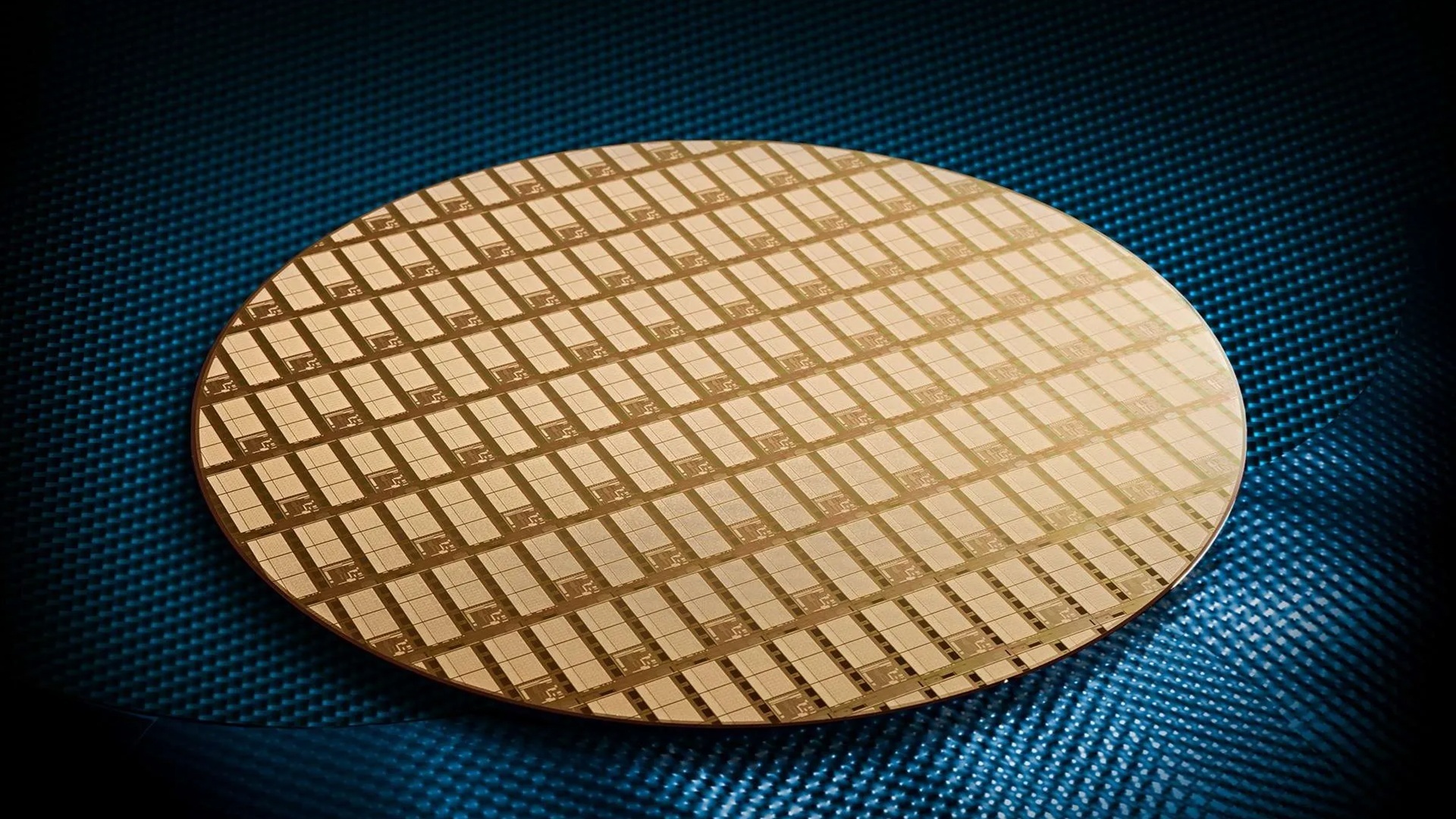
China cuts photonic chip costs by 90% using nanoscale stamping on eight-inch wafers

A Chinese startup has claimed a breakthrough in photonic chip manufacturing by producing 8-inch optical chip wafers without relying on conventional deep ultraviolet (DUV) lithography systems.

Hangzhou-based Prinano said it successfully validated mass production of photonic chips using its nanoimprint lithography (NIL) technology, a manufacturing approach that physically stamps nanoscale patterns onto wafers instead of projecting them through optical systems.

According to the company, the process was carried out in collaboration with Shenzhen Litra Technology and used its PL-AS vacuum air-cushion nanoimprint lithography equipment. Prinano said the method “completely avoids” the need for DUV lithography tools while reducing manufacturing costs to about one-tenth of traditional solutions.

The announcement comes as Chinese chipmakers continue looking for alternative manufacturing technologies amid restrictions on access to advanced lithography systems from Dutch supplier ASML.

Seeking lithography alternatives

Photonic chips are used in applications such as optical communications, sensing systems, lidar, and data centers. Unlike conventional electronic chips, they process information using light rather than electrical signals.

Prinano said its technology supports wafer-level production of photonic chips and can be applied to optical communication and sensing devices based on gallium arsenide, indium phosphide, and silicon photonics.

The company said its PL-AS tool offers sub-10-nanometer line-width resolution along with wafer-level pressure control. However, it did not disclose production volumes, manufacturing yields, or customer shipment data.

Nanoimprint lithography has long been viewed as a potential alternative to traditional optical lithography because it can create extremely fine features without the need for expensive projection optics. The technology was pioneered in the 1990s by Princeton University professor Stephen Y. Chou.

Prinano founder Ge Haixiong studied under Chou and established the company in 2017 to develop NIL equipment, materials, and manufacturing processes.

Questions over scalability

Interest in nanoimprint lithography has increased in recent years as chipmakers seek lower-cost manufacturing methods. In 2023, Canon introduced a commercial NIL system and promoted it as an alternative to some advanced lithography tools.

Despite the promise, analysts have questioned whether the technology can match the throughput and yields required for large-scale semiconductor manufacturing.

Research firm SemiAnalysis has previously noted that while NIL equipment can be cheaper than advanced lithography tools, overall economics depend on factors such as defect rates, template production, throughput, and process integration.

Prinano’s announcement focuses specifically on photonic chips rather than advanced logic processors, a distinction that may make commercialization more achievable. Photonic devices often rely on repeating nanoscale structures such as gratings, waveguides, and ring resonators, which can be well suited to imprint-based manufacturing.

The company said the technology has moved into wafer-level production validation, but independent verification of yields, commercial deployment, and manufacturing scale has not yet been disclosed.

For China’s semiconductor industry, the development highlights ongoing efforts to explore alternative manufacturing routes as access to advanced lithography equipment remains restricted.

  •  

Google’s DiffusionGemma delivers 4x faster text generation using parallel decoding

Google has unveiled DiffusionGemma, a new experimental AI model that generates text using diffusion rather than the autoregressive approach used by most large language models today. The company says the model can deliver up to four times faster text generation on dedicated GPUs while running on consumer hardware.

The model builds on Google’s Gemma 4 family and Gemini Diffusion research. Unlike traditional language models that generate text one token at a time from left to right, DiffusionGemma creates and refines blocks of text in parallel.

According to Google, the approach enables output speeds exceeding 1,000 tokens per second on an NVIDIA H100 GPU and more than 700 tokens per second on an NVIDIA GeForce RTX 5090.

The company says DiffusionGemma is aimed at developers working on speed-sensitive applications such as interactive editing, rapid content iteration, code infilling, and other workflows where low latency is more important than maximum output quality.

Breaking text bottlenecks

Most large language models generate text sequentially, predicting one token after another. While effective, this process can leave local hardware underutilized when serving a single user.

DiffusionGemma takes a different approach. Instead of generating text word by word, it creates a 256-token block at once and then repeatedly refines it through multiple passes.

Google compares the difference to moving from a typewriter to a printing press. Rather than waiting for each token to be generated before producing the next one, the model processes an entire section of text simultaneously.

The company says this shifts the bottleneck from memory bandwidth to compute performance, allowing modern GPUs to operate more efficiently during local inference.

Another key feature is bi-directional attention. Since the model generates text in parallel, every token can attend to every other token during generation. This makes it better suited for tasks where future context matters, such as code completion, in-line editing, mathematical structures, and biological sequences.

Google highlighted a demonstration in which DiffusionGemma was fine-tuned to solve Sudoku puzzles, a task that can be challenging for conventional autoregressive models because later tokens influence earlier decisions.

Designed for local AI

The model uses a 26-billion-parameter mixture-of-experts architecture but activates only 3.8 billion parameters during inference. According to Google, this allows the model to fit within roughly 18 GB of VRAM when quantized, making it accessible on high-end consumer GPUs.

DiffusionGemma also includes an iterative self-correction mechanism. Because it evaluates an entire text block during refinement, it can identify and fix mistakes as generation progresses.

However, Google acknowledged that the model prioritizes speed over quality. The company said standard Gemma 4 models remain the preferred choice for production environments where output quality is the primary concern.

The speed advantage is also most apparent in local deployments and low-concurrency environments. In cloud settings serving large numbers of users simultaneously, conventional autoregressive models can often utilize hardware efficiently through batching, reducing the benefits of diffusion-based generation.

Google has released DiffusionGemma under an Apache 2.0 license through Hugging Face and is supporting deployment through tools including MLX, vLLM, Hugging Face Transformers, NVIDIA NeMo, and Unsloth.

  •  

Lab-aged moon rock offers new clues about how water forms on the lunar surface

Georgia Tech researchers have recreated the effects of solar wind on lunar minerals in a laboratory experiment, providing new evidence that the constant stream of charged particles from the sun plays a major role in shaping the moon’s surface.

The team exposed ilmenite, a mineral commonly found on both Earth and the moon, to a synthetic version of solar wind. The experiment produced nanophase iron, tiny metallic particles that are widely observed in lunar soil and are considered a key signature of space weathering.

Scientists have long known that the moon’s surface is altered by both micrometeorite impacts and solar wind. However, the relative contribution of each process has remained unclear. The new results suggest solar wind alone can create some of the same microscopic features seen in actual lunar samples.

The findings could help researchers better interpret remote sensing data used to estimate the age and composition of the moon’s surface. They may also improve understanding of how lunar soil evolves over time without requiring direct sample collection from every location.

Simulating lunar aging

The research was carried out by physics Ph.D. candidate Roshan Trivedi and recent Ph.D. graduate Advik Vira through the Georgia Tech Center for Lunar Environment and Volatile Exploration Research (CLEVER), a NASA-backed research initiative focused on lunar science and Artemis mission objectives.

Using a vacuum chamber designed to simulate solar wind conditions, the researchers exposed ilmenite samples to charged particles and then examined the material using high-resolution electron microscopy.

The experiment recreated the effects of thousands of years of solar wind exposure in a controlled environment.

The team observed the formation of nanophase iron and lunar-like rims on the mineral surface, features commonly associated with space weathering on the moon.

“Scientists have been doing laboratory radiation experiments for years, but they haven’t been able to characterize the results at this level of detail,” said lead author Trivedi.

The ability to reproduce these features in the laboratory could help scientists better understand how different regions of the moon have changed over time and improve interpretations of orbital observations.

Clues about lunar water

The study may also offer insights into one of lunar science’s most important questions: how water forms on the moon.

Researchers found that the solar wind experiments created tiny voids within the mineral structure. These microscopic spaces could potentially provide locations where hydrogen delivered by solar wind interacts with oxygen present in lunar minerals.

“Water would be a fantastic resource for humans operating on the moon, but scientifically, we are driven simply by the question of how water gets there in the first place,” said Phillip First, a professor in the School of Physics.

“Solar wind is potentially one way, because protons in solar wind provide the hydrogen of H2O molecules while oxygen is present in lunar minerals.”

The researchers say the ability to simulate a wide range of exposure ages could help future studies investigate the connection between solar wind, lunar minerals, and water formation.

“Having the ability to recreate the solar wind and having results look so similar to actual lunar samples is excellent,” said co-lead author Vira.

The findings were published in The Planetary Science Journal.

  •  
❌