❌

Reading view

COXEM Targets HBM Inspection With Atmospheric-Pressure SEM Technology
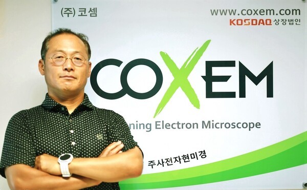
COXEM CEO Lee Jun-hee. (Photo: THE ELEC)

COXEM, a scanning electron microscope (SEM) specialist, is transforming itself into a maker of nondestructive inspection equipment for advanced semiconductor packaging. The company has begun supplying modules for high-bandwidth memory (HBM) analysis and plans to introduce automated inspection equipment for panel-level packaging (PLP) and glass substrates.

"The ion beam polisher, which precisely polishes semiconductor cross sections, was developed into equipment in collaboration with a domestic equipment company," COXEM CEO Lee Jun-hee said in a recent interview at the company's headquarters in Daejeon. "It has already been supplied to major semiconductor manufacturers and is undergoing mass-production evaluations."

COXEM, founded in 2007, is a South Korean developer and manufacturer of SEMs. The company started by licensing technology from the Korea Research Institute of Standards and Science (KRISS). It localized compact tabletop SEMs in the early 2010s and ranked fifth globally in sales in 2022, establishing its competitiveness in the market.

Lee, who holds a doctorate in electrical and electronic engineering from the Korea Advanced Institute of Science and Technology (KAIST), joined COXEM as head of its research center in 2010 and led research and development (R&D) of the technology. Lee was recognized for his technology development capabilities and business planning skills in 2012.

Ion Beam Polisher Module for HBM, MLCC Targets Qualification Early Next Year
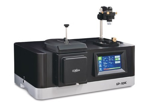
COXEM's IP-10K ion beam polisher. (Photo: COXEM)

An ion beam polisher is preprocessing equipment used to etch and polish a sample before it is examined with an electron microscope. It is based on ion miller commercialization technology that COXEM completed in 2019. COXEM's ion gun module, which emits an argon (Ar) ion beam, is installed inside the equipment. A separate SEM is also installed to observe and analyze the sample after preprocessing. AP Systems handles assembly and sales of the complete equipment.

Semiconductor analysis laboratories have traditionally polished sample cross sections manually, mainly using blades or sandpaper. The ion beam polisher automates the process. It uses a nanometer-scale particle beam to create flat cross sections without errors. It also minimizes sample damage and contamination compared with chemical mechanical polishing (CMP), preserving the sample's fine structures.

The system is similar to focused ion beam-scanning electron microscope (FIB-SEM) systems from global competitors such as Thermo Fisher Scientific and ZEISS, but differs in processing area and speed. FIB-SEM can precisely process extremely small areas of several micrometers or less and is suited to detailed analysis of nanoscale defects.

The ion beam polisher can rapidly remove material across areas as wide as several millimeters at a rate of 1,000 micrometers per hour. It can be used to inspect structures and defects including through-silicon vias (TSVs) and microbumps in HBM, as well as internal layers of multilayer ceramic capacitors (MLCCs). It is also less expensive. COXEM's CP-SEM lineup combining an ion miller and SEM costs about one-tenth as much as competing FIB-SEM systems.

"We initially guaranteed 100 hours of durability for the ion gun module, but have increased that to several thousand hours to meet the requirements of actual semiconductor mass-production lines," Lee said. "We expect to pass customer qualification tests around the end of this year or early next year and move into mass-production supply."

Nondestructive Inspection Equipment for Large Substrates Under Development
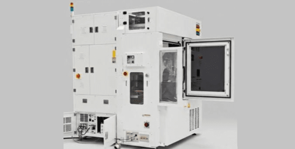
COXEM's Eirtron automated inspection equipment under development. (Photo: COXEM)

COXEM is also preparing semiconductor inspection equipment under its Eirtron brand. The equipment is designed for nondestructive observation of large-area samples, including wafers, large panels and glass substrates, during manufacturing. It is based on atmospheric-pressure scanning electron microscope (A-SEM) technology developed by COXEM.

Conventional inspection of large substrates requires cutting cross sections and moving them to an analysis laboratory. This is because conventional SEMs used for inspection rely on sealed high-vacuum chambers, limiting sample size. SEMs inspect samples by analyzing signals reflected from an irradiated electron beam. If the beam collides with air particles and scatters, the signal weakens and the detected image becomes blurred. High-vacuum chambers are used to prevent this.

A-SEM addresses this issue while maintaining high-resolution imaging with 30-nanometer resolution. This is achieved by completely separating the electron column, including the electron gun that emits the beam, from the external environment using a graphene membrane.

Graphene has high electron transmittance, allowing the beam to pass while blocking outside air. A multi-window structure allows it to withstand pressure of one atmosphere. The graphene membrane and signal detector are positioned as close as possible to the sample, while helium gas is injected to minimize electron-beam scattering and signal loss. These are all proprietary technologies patented by COXEM.

A-SEM can observe samples in ambient air at atmospheric pressure, eliminating size restrictions. It also removes the need for complex preprocessing steps such as evacuating a vacuum chamber or cutting samples, helping reduce process time.

"A-SEM technology enables real-time observation and analysis on production lines without damaging samples, making it an innovation that could shift the paradigm of semiconductor inspection processes," Lee said. "By commercializing automated A-SEM equipment, we aim to take the lead in the semiconductor equipment market currently dominated by overseas companies such as Applied Materials and Hitachi."

A test model of COXEM's automated equipment is currently undergoing validation by a major South Korean substrate company. The company plans to expand its target customer base to outsourced semiconductor assembly and test (OSAT) companies.

  •  

YMC Plans at Least 15 Billion Won in Dividends Over Three Years

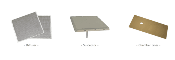
Equipment components made by YMC. (Source: YMC)

YMC, a maker of components and materials for semiconductor and display equipment, plans to distribute at least 15 billion won in dividends to shareholders over three years starting this year.

YMC disclosed the shareholder value enhancement plan on Sept. 16. The company updated a plan announced in April, setting numerical targets for shareholder returns.

YMC will use 30% of net income as a source for dividends. It also set a minimum dividend level. The company plans to pay at least 5 billion won annually from this year through 2028, for a cumulative total of at least 15 billion won over the three years.

The company will also continue to cancel treasury shares. YMC canceled 500,000 treasury shares in March and plans to cancel at least another 630,569 shares by year-end, equivalent to about 50% of the 1,261,138 shares it currently holds. If completed as planned, the total number of shares outstanding will decline by at least 3.32%. Including shares canceled in February 2023, cumulative cancellations are expected to exceed 1.63 million shares.

YMC has also established a system to monitor implementation of its shareholder value enhancement plan. The company will carry out the plan under the management and supervision of its board and conduct a self-assessment at least once a year, disclosing its implementation status. It also plans to expand investor communications through domestic and overseas investor relations events and press releases.

"The shareholder value enhancement plan demonstrates our strong confidence in improving the company's future performance and our commitment to shareholder returns," YMC said. The company posted consolidated revenue of 100.5 billion won and operating profit of 3.89 billion won in the first half of 2026, up 19.2% and 55.3%, respectively, from a year earlier. A new semiconductor plant in Dangjin, South Chungcheong Province, completed last year, began full-scale mass production this year, driving revenue growth and improved profitability.

YMC manufactures and supplies diffusers and susceptors for chemical vapor deposition (CVD) equipment as well as vacuum equipment components. Diffusers uniformly distribute gas inside process equipment chambers to help form even thin films on treated surfaces or facilitate etching. Susceptors support wafers or substrates to maintain uniform temperatures during thin-film deposition.

  •  

Novathermo Expands AI Chip Thermal Materials, Targets 36 Billion Won in Sales

Novathermo CEO Kim Hyung-chul. (Photo: Novathermo)

Novathermo, a thermal management materials startup, is focusing its resources on thermal materials for artificial intelligence (AI) semiconductors and automotive electronics. Following the commercialization of a high-thermal-conductivity material for printed circuit boards (PCBs), the company has added silicone thermal pads to its product lineup. It aims to reach 36 billion won in sales by 2030.

Kim Hyung-chul, CEO of Novathermo, said on Sept. 16 that PCB thermal materials require significant time for final validation because they undergo multiple processes while still in a semi-finished state, while thermal interface material (TIM) silicone pads can be evaluated by customers in a form close to the finished product after production and before shipment.

"It is significant because this is our first commercial product line that expands our thermal management technology into the TIM market, where demand is substantial," Kim said.

Novathermo develops and produces new polymer-based thermal materials using carbon nanotubes (CNTs). Its main products are designed to rapidly transfer heat generated by semiconductors and automotive electronic components while maintaining electrical insulation. The company is developing thermal materials for PCBs, semiconductor packaging and power electronics.

Its core technology involves uniformly dispersing highly thermally conductive materials such as CNTs and alumina within polymers. Novathermo uses a high-shear mixing process to reduce material agglomeration and create pathways for heat transfer. The technology is designed to improve thermal performance while maintaining electrical insulation and mechanical strength.

Its flagship product is Aqua, a high-thermal-conductivity material for PCBs. PCBs are substrates that connect semiconductors and other electronic components. Aqua enables the PCB material itself to conduct heat efficiently, allowing heat generated by chips to dissipate through the substrate as well.

Heat generated by semiconductors is typically removed through heat sinks or cooling systems positioned above the chip. Aqua adds another heat-transfer path through the underside of the substrate. In Novathermo's own tests, replacing only the material with Aqua while keeping the substrate thickness and component configuration unchanged reduced chip temperatures by as much as 30% and substrate temperatures by 20%. The product was commercialized in November last year.

The material achieves thermal conductivity of about 2 watts per meter-kelvin (W/m·K) on mass-production equipment. Novathermo has achieved up to 3.3 W/m·K at the laboratory stage. Thermal conductivity measures how effectively a material transfers heat, with higher values indicating faster heat transfer.

Novathermo has also completed customer validation for automotive components. In a comparison of identical circuits using different PCB materials in an automotive lidar module, Aqua lowered the temperature of the transmitter (Tx) chip by more than 10 degrees Celsius compared with the conventional material. The company said that exceeded the customer's initial target of a 4-degree reduction.

The company is also conducting proof-of-concept (PoC) projects with global companies. PoC involves applying the material directly to a customer's product to determine whether it meets required performance specifications. Successful validation could lead to additional reliability testing and discussions on mass-production supply.

Novathermo has also introduced FLEXURE, a silicone thermal pad brand. It has established mass-production capabilities for products with thermal conductivity ratings of 3, 5 and 8 W/m·K. The company has also completed prototype design for a high-performance 12 W/m·K product line.

FLEXURE is placed between a semiconductor chip and a heat sink. Microscopic gaps form between the surfaces of the chip and heat sink, and air trapped in those spaces can impede heat transfer. The silicone pad fills the gaps, transferring heat generated by the chip to the heat sink.

A key challenge in product development is achieving both thermal performance and suitable physical properties. Adding more filler to increase thermal conductivity can make a pad harder or more prone to tearing while reducing its ability to conform to component surfaces. Novathermo adjusted the filler composition, silicone structure, cross-linking and molding processes to improve thermal conductivity, dimensional stability and surface conformity.

Novathermo plans to expand its customer base in semiconductor packaging, power electronics and automotive electronics, centered on its high-thermal-conductivity PCB materials and silicone TIM pads. Its current mass-production yield is about 70%.

The company also plans to expand production capacity. Monthly output is targeted to rise from 10,000 panels this year to 1.2 million panels in 2030. Over the same period, the number of key customers is expected to increase from three to 25, while exports are targeted to rise from 10% to 55% of sales. Novathermo aims for 36 billion won in revenue by 2030.

"Customers requesting samples are focusing not only on thermal performance but also on the pads' ability to resist tearing and maintain surface conformity even under high-hardness conditions," Kim said. "We will improve product quality and mass-production reliability to help localize high-performance thermal materials that are heavily dependent on overseas suppliers and stabilize the supply chain."

  •  

HD Construction Equipment Wins Order for 45 Excavators in Hong Kong

HD Construction Equipment’s 53-ton DEVELON DX530 excavator.

HD Construction Equipment will supply 45 mid- to large-sized excavators for a railway extension project in Hong Kong.

HD Construction Equipment said on Sept. 16 it will supply 45 DEVELON excavators for the Tung Chung Line Extension project led by MTR Corporation.

The order consists of seven 53-ton large excavators and 38 mid- to large-sized excavators ranging from 14 to 36 tons.

The equipment will be deployed for construction of a new station and an approximately 1.2-kilometer railway extension. As the construction site is located on reclaimed coastal land, demand is also expected for specialized equipment such as long-reach arms for extended-range operations.

Including this order, HD Construction Equipment has sold 75 excavators in Hong Kong this year. The company plans to increase annual sales in the market to more than 100 units by 2029.

  •  

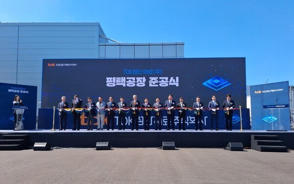
TOK Completes Pyeongtaek Poseung Plant

TOK's Pyeongtaek Poseung plant completion ceremony on Sept. 15. (Photo: Gyeonggi Province)

Japan's Tokyo Ohka Kogyo (TOK) held a completion ceremony on Sept. 15 for its manufacturing facility in the Poseung district of Pyeongtaek, Gyeonggi Province. About 100 officials attended, including Gyeonggi Free Economic Zone Authority Commissioner Kim Neung-sik, Pyeongtaek Mayor Choi Won-yong, TOK President Noriaki Taneichi and TOK Advanced Materials CEO Kim Ki-tae.

TOK Advanced Materials will invest a total of 101 billion won on a 55,560-square-meter site to establish a high-purity chemical manufacturing facility in the first phase. The company also plans to build photoresist (PR) production capacity in the future. Of the total investment, 70.6 billion won is foreign direct investment. The project will create about 70 new jobs.

TOK Advanced Materials is the Korean subsidiary of TOK. TOK is the market leader in photoresists, supplying products to Samsung Electronics, SK hynix, TSMC and Intel. Photoresist is a key material used to form circuit patterns on silicon wafers during semiconductor patterning.

The project follows a memorandum of understanding (MOU) signed in April 2023 after the Gyeonggi Free Economic Zone Authority visited TOK's headquarters in Kanagawa Prefecture, Japan. The two sides discussed cooperation aimed at attracting a world-class semiconductor materials production base. The plant was completed three years after the investment was secured.

Gyeonggi Province has what it describes as the world's largest semiconductor cluster, linking semiconductor industry hubs including Pyeongtaek's Poseung and Hyeondeok districts with Yongin, Icheon, Hwaseong and Anseong. The Poseung and Hyeondeok districts are expected to become a hub for advanced materials within the semiconductor belt.

"Semiconductors are a strategic high-tech industry that determines national competitiveness," Kim Neung-sik said. "The completion of TOK's plant will help the region emerge as a hub for key semiconductor materials."

  •  

Orchem Unveils TGV Plating, Adhesion Technologies for Glass Substrates

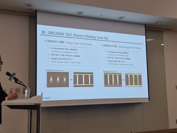
An Orchem official explains the company's ZENITH-1000 and ZENITH-1500 chemicals used for bridge-fill and side-up TGV plating at a technical seminar during KPCA Show 2026 on Sept. 10. (Photo: THE ELEC)

Orchem has introduced two plating approaches for metallizing through-glass vias (TGVs) in glass substrates. The company also unveiled a wet-process adhesion technology designed to improve bonding between glass and copper and between glass and insulating layers.

Orchem introduced its TGV plating and wet seed layer technologies at a technical seminar held during KPCA Show 2026 at Songdo Convensia in Incheon on Sept. 10. The company specializes in plating and surface-treatment chemicals used in semiconductor packaging and printed circuit board (PCB) manufacturing.

Orchem has developed two TGV plating approaches depending on substrate thickness and hole diameter. One is the bridge-fill method, commonly called center fill, which first forms a copper bridge at the center of the TGV hole and then fills the spaces above and below it. The other is the side-up fill method, which grows copper from the hole sidewalls toward the center.

The bridge-fill method uses Orchem's ZENITH-1000 plating solution. Filling the spaces above and below the copper bridge separately shortens overall plating time. The method is suited to TGVs with a low aspect ratio (AR). As substrates become thicker or hole diameters smaller, however, a higher AR can result in deeper enclosed holes, or blind vias, above and below the copper bridge.

ZENITH-1500 is used for side-up fill, in which copper grows across the entire TGV sidewall until the copper layers meet at the center. The approach can reduce void formation in high-AR TGVs. Orchem has completed plating evaluations on glass substrates up to 1 millimeter thick and is evaluating smaller hole diameters with aspect ratios of up to 20:1. Because copper grows across the entire hole sidewall, however, a thicker copper layer also forms on the substrate surface and plating takes longer.

Orchem has also developed an adhesion promoter (AP) to improve bonding between glass and copper or between glass and Ajinomoto Build-up Film (ABF). Glass has lower surface roughness than organic substrates, making it difficult to achieve sufficient adhesion. Palladium (Pd) catalysts used in electroless plating also have difficulty bonding copper to the glass surface.

The company synthesized the AP based on 3-aminopropyltriethoxysilane (APTES), a conventional silane-based adhesion material, by increasing the number of functional groups and molecular size. It is designed with separate functional groups that bond to glass and to copper or ABF, improving adhesion. The adhesion promoter can be wet-coated onto the glass surface before electroless copper plating. The coating is less than 100 nanometers thick.

Orchem also plans to commercialize bottom-up plating and a sputter-less process. Bottom-up plating grows copper from the bottom of a TGV hole and can reduce void formation even at high aspect ratios. The company is currently evaluating technology to uniformly form a seed layer at the bottom of the hole. The sputter-less process uses an adhesion promoter and electroless plating to form a copper seed layer without conventional sputtering. Orchem plans additional evaluations and aims to commercialize the adhesion material for the sputter-less process by year-end.

"TGV plating chemicals have already reached the commercialization stage," an Orchem official said. "Development of the adhesion material for the sputter-less process is complete, and our goal is to commercialize it by year-end after additional evaluation and validation."

  •  

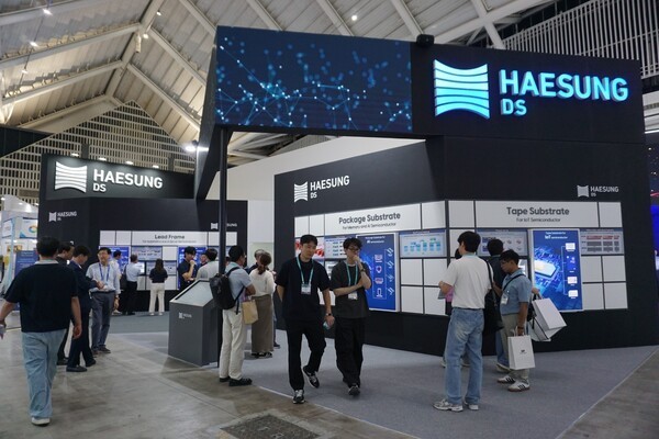
Haesung DS Showcases Three Semiconductor Substrate Technologies

Haesung DS participates in KPCA Show 2026. (Photo: Haesung DS)

Haesung DS said it showcased semiconductor substrate products including lead frames, package substrates and tape substrates at KPCA Show 2026 at Songdo Convensia in Incheon.

Lead frames are metal substrates that connect semiconductor chips to external circuits and provide structural support. Package substrates transmit electrical signals between semiconductor chips and mainboards. Tape substrates are thin-film substrates used for packaging components such as display driver integrated circuits (DDIs).

Haesung DS has participated in the event annually since 2023, presenting its key products and technologies. The company uses the exhibition to share technology and market trends with Korean and overseas customers and industry officials and explore potential business cooperation.

Haesung DS CEO Choi Young-sik received the Best Pathfinder Award at this year’s event in recognition of his active corporate management and commitment.

“We were able to introduce our technologies to industry officials,” a Haesung DS official said. “We will continue to strengthen our technological competitiveness and production capabilities to proactively respond to market and customer needs and actively identify new growth opportunities.”

  •  

CK Solution Expands AI Data Center Business With Schneider Electric

CK Solution is expanding its artificial intelligence (AI) data center business with global energy management and automation company Schneider Electric. The company plans to broaden its data center capabilities by adding power and automation solutions to its existing HVAC and cooling business.

CK Solution said it signed an agreement to become an authorized distributor for Schneider Electric in Korea. CK Solution will supply Schneider Electric's AI data center solutions in the Korean market and provide technical support and services.

Schneider Electric offers power infrastructure and cooling solutions for data centers, including switchgear, uninterruptible power supplies (UPS), transformers and automation systems. It also supplies software including digital twins and data center infrastructure management (DCIM) systems.

The company is also developing high-density power and cooling technologies for AI data centers with Nvidia and other major graphics processing unit (GPU) companies. It is also working with SK Telecom on the SK AI Data Center Ulsan project.

CK Solution has been expanding its data center business based on HVAC technology developed for semiconductor cleanrooms and battery dry rooms. After establishing a data center business division last year, it secured telecommunications and information and communications technology (ICT) companies as customers. It also partnered with LG Electronics in data center HVAC solutions.

The company has also been building its order backlog. In June, CK Solution signed a 9.2 billion won contract with Hanwha Systems to build data center cooling facilities and a building management system (BMS). The contract runs through March next year.

CK Solution plans to use the Schneider Electric distributor agreement to expand its data center business from cooling and HVAC into power infrastructure and automation. It aims to secure new customers by combining its design and construction experience with Schneider Electric's solutions.

  •  

Murata to Mass-Produce iPaS for AI Chips Next Year

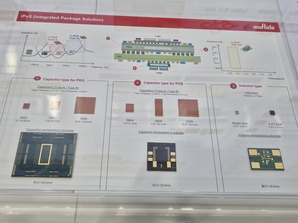
Korea Murata Electronics displayed iPaS at KPCA Show 2026 on Sept. 9. (Photo: THE ELEC)

Murata, the world's largest maker of multilayer ceramic capacitors (MLCCs), plans to begin mass production next year of its Integrated Package Solution (iPaS), a power substrate for artificial intelligence (AI) semiconductors. Major customers are expected to be big tech companies developing AI chips. Murata is expanding its AI power solutions from passive components such as MLCCs and silicon capacitors to substrate-based products.

Murata showcased iPaS at KPCA Show 2026 at Songdo Convensia in Incheon on Sept. 9. Instead of mounting individual capacitors or inductors on a substrate, iPaS integrates their functions into an ultra-compact multilayer substrate. The units can be arranged in arrays, allowing capacitance, electrical characteristics, dimensions and circuit routing to be customized to customer requirements.

Unlike conventional passive components, iPaS allows circuit wiring to be formed on its surface. Internal vias connect the upper and lower wiring layers, enabling power to be delivered vertically. This reduces the surface area occupied by passive components and frees up space for chip mounting.

Conventionally, power modules are placed around an AI accelerator and supply power through substrate wiring. With iPaS, a power module can be positioned directly beneath an AI accelerator, enabling a vertical power delivery (VPD) architecture. The shorter power delivery path reduces losses.

As AI accelerator computing performance increases, so do power consumption and current requirements. Supplying large currents reliably within limited space makes reducing the distance between the power module and AI semiconductor increasingly important. iPaS supports high-density power architectures by reducing the space occupied by passive components while enabling vertical power delivery.

Major customers are expected to include hyperscalers and other big tech companies. As a high-value product, iPaS is expected to be used primarily in high-end products such as AI accelerators rather than general-purpose semiconductors.

"It is a high-priced product, so our customers will be big tech companies rather than makers of general-purpose products," a Murata official said. "It should be in mass production next year."

Murata is developing iPaS in capacitor and inductor versions. The capacitor type integrates high-capacitance functionality into the substrate, reducing the number of surface-mounted MLCCs. The inductor type integrates coil functionality into the substrate to support high-current delivery. Murata also plans to develop a product combining capacitor and inductor functions on a single substrate.

Murata has been developing iPaS for AI and high-performance computing (HPC) applications for several years. It first unveiled samples at FLEX Japan in 2023 and demonstrated a power module using iPaS at the Electronic Components and Technology Conference (ECTC) in 2024. The module reduced the number of surface-mounted capacitors by more than 60% while maintaining voltage fluctuation characteristics similar to conventional designs. Murata has discussed product adoption with graphics processing unit (GPU) and AI accelerator customers, targeting commercialization in 2026.

Murata plans to develop iPaS into a next-generation growth product, targeting annual sales of 50 billion yen within 18 months of mass production. That would be equivalent to about 5% of its capacitor sales of 936.4 billion yen in fiscal 2025, which ran from April 2025 through March 2026.

  •  

Simmtech Wins Three Awards at KPCA Show

Simmtech Vice President Park Min-ho. (Photo: Simmtech)

Simmtech was recognized for its mass-production achievements in Small Outline Compression Attached Memory Module (SOCAMM), a next-generation memory module for artificial intelligence (AI) servers, with three employees and executives receiving industry awards.

Simmtech said Vice President Park Min-ho received the Minister of Trade, Industry and Resources Award at the KPCA Show 2026 reception and awards ceremony held at Songdo Convensia in Incheon on Sept. 9. Park was recognized for establishing a SOCAMM mass-production system, contributing to the competitiveness of industries supporting AI semiconductors and strengthening the domestic supply chain.

Simmtech Chief Executive Officer Jeon Young-sun received the Proud Printed Circuit Board (PCB) and Semiconductor Packaging Achievement Award, while senior researcher Yoo Jong-sang received the Proud PCB and Semiconductor Packaging Industry Professional Award.

Simmtech is also showcasing semiconductor substrates for AI servers at KPCA Show 2026, held from Sept. 9 to 11. Products on display include SOCAMM, next-generation Low Power Compression Attached Memory Module (LPCAMM) substrates, enterprise solid-state drive (SSD) modules and Compute Express Link (CXL) memory modules.

"Winning three awards at this year's KPCA Show reflects recognition of Simmtech's leadership in next-generation semiconductor substrates," a company official said. "We will expand investment in advanced packaging substrate technologies, including SOCAMM module substrates and high-layer-count fine-circuit substrates, while strengthening partnerships with global semiconductor manufacturers to solidify our position among the market leaders."

  •  

Duksan Hi-Metal Showcases Solder Ball Technology

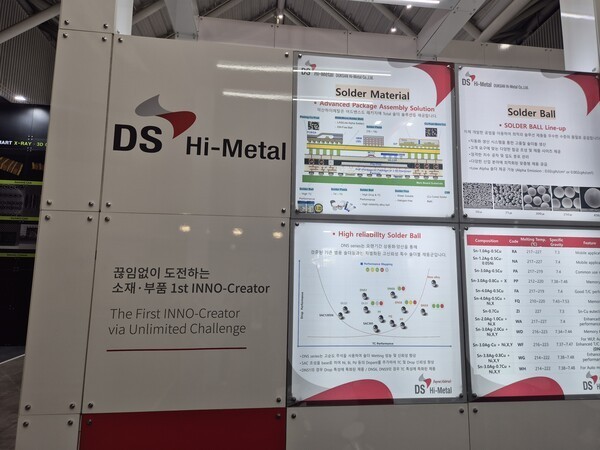
Duksan Hi-Metal displays solder materials at KPCA Show 2026 on Sept. 9. (Photo: THE ELEC)

Duksan Hi-Metal, a semiconductor materials company under Duksan Group, is showcasing solder materials for semiconductors at KPCA Show 2026, held at Songdo Convensia in Incheon from Sept. 9 to 11. The company is strengthening its “total solder solution” business, supplying a full range of materials required for semiconductor bonding.

Solder balls are bonding materials that electrically connect semiconductor chips to substrates. Duksan Hi-Metal holds the largest share of the global solder ball market. As advanced packaging becomes finer with the growth of artificial intelligence (AI) semiconductors and high-performance servers, solder balls are also becoming smaller. Duksan Hi-Metal produces micro solder balls thinner than a human hair with tolerances of several micrometers.

Copper-core solder ball (CSB) products consist of a copper core covered with solder. They use copper’s high thermal conductivity to improve heat dissipation while maintaining a uniform height at package joints.

The company is also displaying solder paste, flux and copper posts (Cu-Post). Solder paste is a cream-like material combining solder powder and flux. Flux removes oxide layers during bonding, helping solder spread evenly across the bonding surface. Cu-Post can replace solder balls and offers high electrical and thermal conductivity, making it suitable for fine-pitch connections.

“This exhibition is an opportunity to showcase increasingly precise next-generation semiconductor interconnect materials based on the technologies we have accumulated over many years,” a Duksan Hi-Metal official said. “We will continue supplying high-performance materials for rapidly growing advanced industries such as AI and lead the global market.”

  •  

Kolon Industries Completes mPPO Plant Expansion

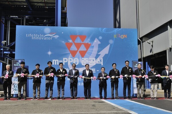
Kolon Industries held a completion ceremony for its mPPO production line at Gimcheon Plant 2 on Sept. 8. (Photo: Kolon Industries)

Kolon Industries said it has completed the expansion of a production line for modified polyphenylene oxide (mPPO), a low-dielectric material used in artificial intelligence semiconductors, and held a completion ceremony on Sept. 8. Attendees included Kolon Industries CEO Huh Sung, Gimcheon Mayor Bae Nak-ho, Gimcheon City Council Chairman Oh Se-gil and Kolon Life Science CEO Lee Hankook.

The company completed the new facilities at its Gimcheon Plant 2 in the second quarter. Production began in the second half after regulatory approvals for hazardous materials and trial operations. Kolon Industries plans to gradually ramp up output through the end of the year.

Kolon Industries’ mPPO offers low-dielectric performance about three to five times higher than epoxy resins used for the same purpose. mPPO is a low-dielectric material used in copper-clad laminates (CCLs), a raw material for semiconductor printed circuit boards (PCBs). Low-dielectric properties that reduce signal loss and heat generation during high-speed signal transmission are important for data-intensive products such as AI accelerators and 6G communications equipment.

The company plans to supply all of the output to global CCL manufacturers. Once trial production is completed and mass production begins in earnest, Kolon Industries expects annual sales from mPPO alone to reach about 200 billion won.

“This expansion marks a turning point for our mPPO business as it enters a full-fledged growth phase,” Huh said. “We will develop next-generation electronic materials into a new growth engine based on differentiated technology and quality competitiveness.”

  •  

Intekplus Wins 6 Billion Won Equipment Order in China

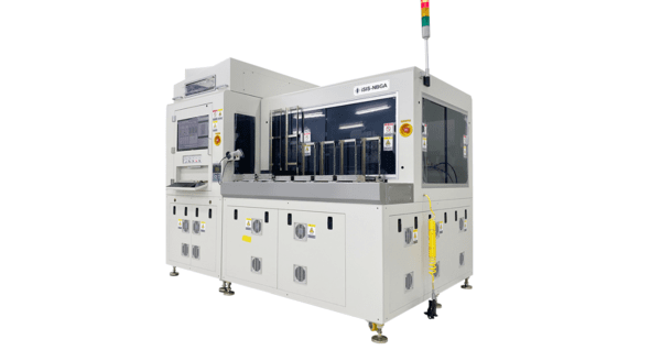
Intekplus’ iSIS-NBGA inspection system. (Photo: Intekplus)

Intekplus will supply about 6 billion won worth of semiconductor and substrate inspection equipment overseas.

Intekplus said in a regulatory filing on Sept. 9 that it signed a contract with ACCUTECH to supply semiconductor and substrate inspection equipment. ACCUTECH is a semiconductor equipment distributor based in Shenzhen, China.

The contract is valued at about 6.08 billion won, equivalent to 6.78% of Intekplus’ 98.77 billion won in revenue last year.

Intekplus will supply two types of equipment from its iPIS series for semiconductor package and chip inspection and its iSIS series for semiconductor mid-end and substrate inspection. The specific models were not disclosed.

The iPIS lineup includes systems for final visual defect inspection of semiconductor packages, 3D dimensional inspection and 2D side inspection. The iSIS lineup includes systems for 3D inspection of microbumps on flip-chip substrates and 3D inspection of bumps and surface defects on flip-chip ball grid array (FC-BGA) substrates.

Payments will be made in four stages. Intekplus will receive 30% of the contract value as an advance payment and another 30% after equipment delivery. A further 30% will be paid after installation and commissioning are verified, with the remaining 10% due after final acceptance. The contract runs through Nov. 30 next year, with the final payment expected before then.

Intekplus recently won an order from a major Japanese substrate manufacturer for automated optical inspection (AOI) equipment used in glass-substrate research and development. The equipment will be delivered in the second half of this year. The number of systems and contract value were not disclosed.

Intekplus posted first-half revenue of 21.77 billion won and an operating loss of 7.03 billion won. Its first-half net loss widened from a year earlier to 7.54 billion won.

  •  

LG Innotek Advances Embedded Substrates With Silicon Capacitors

An embedded substrate sample unveiled by LG Innotek at KPCA Show 2026 on Sept. 9. A silicon capacitor is embedded in the buildup layer. (Photo: THE ELEC)

LG Innotek has unveiled an embedded flip-chip ball grid array (FC-BGA) substrate with silicon capacitors integrated inside the package substrate for artificial intelligence chips. The company is also developing technology to embed active devices and bridges. Demand for embedded substrates, particularly FC-BGAs, is growing as higher-performance AI chips require more stable power delivery.

LG Innotek displayed FC-BGA samples with embedded silicon capacitors at KPCA Show 2026, held at Songdo Convensia in Incheon on Sept. 9. The company showed two structures, with silicon capacitors embedded in either the substrate’s core layer or buildup layer.

The core-layer structure accommodates relatively thick, high-capacitance silicon capacitors. The buildup-layer structure embeds thinner silicon capacitors to reduce overall substrate thickness. LG Innotek said the location and specifications of the embedded silicon capacitors can be varied depending on the semiconductor and substrate design.

A silicon capacitor is a passive component made by forming dielectric and electrode layers on a silicon wafer. It stores power required by a semiconductor and supplies it instantaneously to suppress voltage fluctuations. Conventionally, capacitors are mounted on the substrate surface and deliver power to the chip through copper interconnects. Embedding capacitors inside the substrate shortens the power-delivery distance between the semiconductor and capacitor while freeing up mounting area on the substrate surface.

Silicon capacitors are particularly suited to stable power delivery at high frequencies because of their low equivalent series inductance (ESL). AI semiconductors operate at high speeds and can draw large amounts of power instantaneously. Lower ESL helps suppress voltage fluctuations.

Major silicon capacitor suppliers include Murata and Samsung Electro-Mechanics. TSMC also uses internally produced silicon-based deep trench capacitors (DTCs) in advanced packaging.

LG Innotek has been developing embedding technology for about a decade. It initially embedded multilayer ceramic capacitors (MLCCs) in flip-chip chip-scale packages (FC-CSPs). As the AI semiconductor market expanded, the company unveiled FC-BGA technology with embedded silicon capacitors in 2024 and began applying it to mass-produced products last year.

LG Innotek is also developing technology to embed active devices and bridges inside FC-BGAs, in addition to passive components such as silicon capacitors and inductors. Active devices directly control signals and power, while bridges connect multiple chips over short distances to support high-speed signal transmission. The goal is to expand the substrate’s role beyond simply connecting semiconductors to the mainboard.

“We have applied embedding technology for about 10 years, beginning with passive components inside FC-CSPs,” an LG Innotek official said. “It is attracting renewed attention as FC-BGAs become more advanced.”

“In the past, substrates simply served as a medium for transmitting signals, but they are now evolving to provide functionality themselves by incorporating silicon capacitors, inductors and other components,” the official said. “Moving components from the substrate surface to the inside gives customers greater design flexibility and enables thinner products.”

  •  

Axcelis to Build $35 Million Semiconductor Equipment Plant in Korea

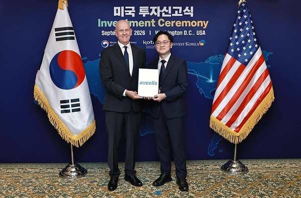
Robert Mahoney, left, Executive Vice President of Global Operations at Axcelis, participates in an investment declaration ceremony. (Photo: Axcelis)

U.S. semiconductor equipment maker Axcelis Technologies said Sept. 8 it plans to build a new equipment manufacturing facility in South Korea with an investment of about $35 million.

Robert Mahoney, Axcelis' Executive Vice President of Global Operations, recently participated in an investment declaration ceremony in Washington, D.C., with officials from South Korea's Ministry of Trade, Industry and Resources (MOTIR) and the Korea Trade-Investment Promotion Agency (KOTRA). The investment totals $35 million.

The new manufacturing facility will be built in Pyeongtaek with a total gross floor area of about 200,000 square feet. The investment is aimed at expanding ion implantation equipment production capacity to meet global demand.

Ion implanters are key front-end semiconductor manufacturing tools that precisely introduce ions into wafers to create desired electrical properties. Axcelis Korea established the Axcelis Asia Operations Center (AAOC) in Pyeongtaek in 2021 and began producing the equipment locally.

The new facility will be designed around a lean manufacturing environment aimed at eliminating waste and maximizing production efficiency. A groundbreaking ceremony is scheduled for Oct. 20, with production targeted to begin in the second half of 2028.

The facility will include Class 1,000 (ISO 6) and Class 10,000 (ISO 7) cleanrooms, a warehouse and a training center. A Class 1,000 cleanroom limits particles measuring 0.5 micrometers (㎛) to no more than 1,000 per cubic foot.

"Ion implanters are among the most important tools in front-end semiconductor manufacturing," Axcelis President and Chief Executive Officer Russell Low said. The investment will strengthen the company's global high-volume manufacturing infrastructure and expand the capabilities needed to serve customers worldwide, he said.

  •  

Taesung Showcases Three TGV Process Systems at KPCA Show 2026

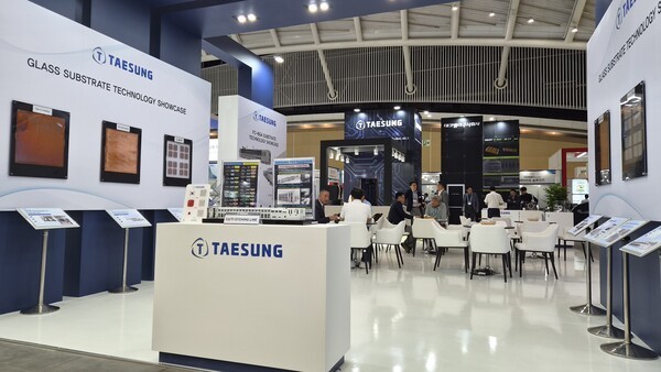
Taesung is showcasing its glass substrate production equipment technology at KPCA Show 2026. (Photo: Taesung)

Taesung said Sept. 9 it is showcasing glass substrate production equipment technology at the International Semiconductor Substrate & Advanced Packaging Industry Exhibition, or KPCA Show 2026.

KPCA Show is a South Korean exhibition specializing in printed circuit boards (PCBs) and semiconductor packaging. The event is being held Sept. 9-11 at Songdo Convensia in Incheon. Taesung is presenting process technologies optimized for glass substrates, including etching, cleaning and plating, at its booth.

In particular, the company is showcasing key equipment for the Through Glass Via (TGV) process. TGVs are tiny holes formed in glass substrates to create electrical signal paths between chips and substrates. Taesung is displaying etching equipment that shapes and refines the holes, cleaning equipment that removes contaminants and plating equipment that coats the holes with metal to enable electrical conductivity.

Taesung has developed equipment for each stage of glass substrate processing based on technology accumulated in its existing PCB manufacturing equipment business. The company is targeting the market with mass-production solutions tailored to different manufacturing methods and process conditions for individual customers. Supply discussions with major customers are currently in their final stages, and Taesung expects to secure new orders within this month.

"Global demand for glass substrates is growing as AI semiconductors become more powerful and advanced packaging technologies develop," Taesung said. "We will actively showcase our differentiated process equipment technology at KPCA Show."

The growing AI and high-performance computing (HPC) markets are also increasing the importance of next-generation semiconductor packaging technologies. Glass substrates, a next-generation packaging material, have flatter surfaces than conventional substrates made of plastic or organic materials, making them better suited for denser, finer circuit patterns. They are also less susceptible to warpage and deformation caused by heat.

  •  

Simmtech Showcases Next-Generation AI Substrate Technology

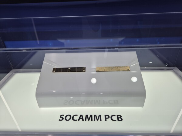
A SOCAMM module printed circuit board (PCB) displayed by Simmtech at KPCA Show 2026 on Sept. 9. (Photo: THE ELEC)

Simmtech is showcasing next-generation semiconductor substrate technologies, including Small Outline Compression Attached Memory Module (SOCAMM) for artificial intelligence servers, at KPCA Show 2026, held Sept. 9-11 at Songdo Convensia in Incheon.

Key products on display include SOCAMM, next-generation Low Power Compression Attached Memory Module (LPCAMM), enterprise solid-state drive (SSD) modules and Compute Express Link (CXL) memory modules.

Simmtech is the largest supplier of module printed circuit boards (PCBs) and memory semiconductor package substrates used in SOCAMM. Nvidia's Rubin CPU uses eight SOCAMMs, with each SOCAMM containing four low-power DRAM (LPDDR) packages. Simmtech supplies both SOCAMM module PCBs and LPDDR package substrates.

The company is also showcasing ultra-thin and ultra-fine substrate technologies, including Ultra-Thin Substrate, Hybrid Substrate, Small Via, Fine Bond Finger and Fine-Pitch/Dual-Size Small Outline Package (SOP) technologies.

Simmtech is displaying substrate technologies designed to address rising power consumption and heat generation in AI semiconductors. Bar Via, Chunk Via and Thick Cu Pattern technologies improve heat dissipation for high-power semiconductors. The company is also showcasing Rigid-Flex Substrate using Cu Post and Cavity technologies, as well as Wettable Flank substrates.

Simmtech is also presenting preliminary research on glass substrates, a technology that replaces conventional organic cores with glass. The technology can reduce warpage in large-area packages while facilitating ultra-fine wiring and improving signal integrity.

"The importance of substrate technology is greater than ever as the AI semiconductor market grows," a Simmtech official said. "Through this exhibition, we will share our next-generation semiconductor substrate technologies and future vision with customers and industry officials and strengthen our technology leadership in the global market."

  •  

TLB Selected as Lead Factory for Ansan AI Transformation Project

TLB headquarters. (Photo: TLB)

TLB will introduce artificial intelligence (AI)-based smart manufacturing technologies at its printed circuit board (PCB) production plant in Ansan. The company will use AI to optimize production conditions and deploy autonomous mobile robots and other technologies on the factory floor.

Ansan City said Sept. 8 that it will develop TLB into a lead AI factory as part of its AI transformation (AX) demonstration industrial complex project at the Banwol and Sihwa National Industrial Complexes. The technologies will first be demonstrated at TLB’s Ansan plant before successful applications are expanded to other manufacturers in the industrial complexes.

The AX demonstration industrial complex project integrates AI and data into manufacturing processes to improve productivity, reduce costs and strengthen corporate competitiveness. A total of 28 billion won in central government, local government and private funding will be invested through 2028.

The project will also establish a manufacturing AI open lab where companies can directly test AI technologies. Universities and research institutions will analyze problems at manufacturing sites and develop and demonstrate the necessary technologies. An AX comprehensive support center will assess each company’s level of AI adoption and connect it with appropriate technologies and experts. Plans also call for a secure data zone where manufacturing, energy and logistics data can be used, as well as an integrated support platform linking manufacturers with AI technology companies.

“The Banwol and Sihwa industrial complexes have been a key foundation supporting Ansan’s industrial competitiveness, and we need to transform them into future-oriented industrial complexes through manufacturing innovation and improvements to working conditions,” Ansan Mayor Lee Min-geun said. “We will create a virtuous cycle in which production innovation using AI and data strengthens corporate competitiveness, while a better working environment attracts young people and talent.”

  •  

DRT Commercializes Multi-Stage Pyrolysis Technology for Battery Recycling

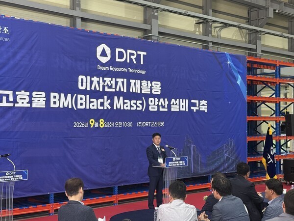
DRT CEO Jung Chul-won delivers remarks at an event marking the completion of a waste battery recycling mass-production facility at the Saemangeum Industrial Complex in Gunsan, North Jeolla Province, on Sept. 8. (Photo: THE ELEC)

Battery recycling startup DRT has commercialized its proprietary multi-stage pyrolysis technology.

The company built its first mass-production facility at the Saemangeum Industrial Complex in Gunsan, North Jeolla Province, applying its technology to actual waste battery processing. Compared with conventional rotary kiln systems, the technology reduces both energy consumption and carbon dioxide emissions by about 50%.

DRT held an event on Sept. 8 at the Saemangeum Industrial Complex to mark the completion of its battery recycling mass-production facility. The first production line can process 12,000 tons of waste batteries annually, equivalent to batteries used in about 24,000 electric vehicles.

The first production line unveiled at the event integrates equipment for dismantling EV battery packs into modules and cells, crushing and heat treatment, and separation of black mass (BM), a powder containing valuable metals, within a single building. South Korean automation equipment maker Toptec supplied the automated equipment for separating battery packs, modules and cells. DRT designed and manufactured the core equipment for subsequent processes, including crushing and heat treatment.

The company plans to add production lines at its Gunsan plant after reviewing operations of the first line and customer demand. It is considering building second and third lines of the same capacity on the remaining site. If all three lines are operational, the Gunsan plant is expected to generate more than 20 billion won in annual revenue.

“This is a mass-production facility incorporating our independently developed high-efficiency resource recovery technology,” DRT CEO Jung Chul-won said. “We will use the first line as a global standard model for mass production and expand our business with customers in South Korea and overseas.”

A key feature of DRT’s system is its ability to process both waste batteries and low-grade black mass on a single line. Waste batteries undergo crushing, heat treatment and separation to recover powder containing valuable metals, while low-grade black mass containing residual organic materials and impurities is heat-treated again to improve its quality.

At the core is DRT’s proprietary multi-stage pyrolysis technology. After waste batteries are crushed, nitrogen is used to lower the oxygen concentration before the material is heat-treated at about 500 degrees Celsius. Organic materials such as electrolytes, separators and binders are removed in a sealed, multi-stage reactor. The process reduces fire risk while increasing black mass purity to about 98%.

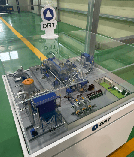
A model of DRT’s first waste battery recycling mass-production facility at the Saemangeum Industrial Complex in Gunsan, North Jeolla Province. (Photo: THE ELEC)

DRT will use the first production line to process waste batteries and black mass supplied by customers on a contract-processing basis. Annual revenue is expected at 7 billion to 7.5 billion won. Unlike conventional recyclers that directly purchase raw materials and sell the resulting black mass, DRT processes materials secured by its customers and receives a processing fee.

DRT chose this business model because it allows the company to turn existing recyclers into customers rather than compete with them for waste battery feedstock. By processing customer materials in Gunsan, DRT plans to demonstrate the performance and economics of its multi-stage pyrolysis equipment and expand into an equipment business that installs the technology on customers’ production lines. Each equipment sale could generate tens of billions of won in revenue.

DRT is in discussions with companies in the US and Japan to supply its multi-stage pyrolysis equipment. It is also discussing businesses using waste battery recycling equipment with battery materials companies in South Korea and overseas.

DRT is expanding its pyrolysis technology developed for waste batteries into areas including biomass and waste plastics.

In biomass, the company is developing technology to pyrolyze woody and herbaceous feedstocks to produce bio-oil for use as a feedstock for sustainable aviation fuel (SAF).

DRT is also advancing catalytic pyrolysis technology for waste plastics. The technology converts waste plastics through pyrolysis into feedstocks for high-value chemical products. DRT is participating in government-funded research projects with universities, refiners and chemical companies to develop the technologies.

DRT has also secured external funding for technology development and construction of mass-production facilities. It has raised 5 billion won since its establishment. Following the start of operations at its first production line, the company plans to secure additional funding to build more facilities and commercialize its pyrolysis technologies.

  •  

Simmtech Signs Long-Term Supply Deals With Key Partners

Simmtech CEO Chun Youngsun. (Photo: Simmtech)

Simmtech is strengthening cooperation with key domestic and overseas suppliers. The company signed long-term supply agreements with some partners to address uncertainty in raw material procurement.

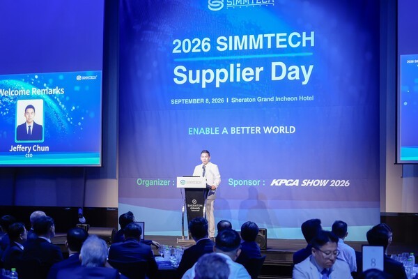
Simmtech said Sept. 8 that it held its 2026 Simmtech Supplier Day at the Sheraton Grand Incheon Hotel in Songdo. The event was attended by 34 representatives, including chief executives and sales executives, from 17 major domestic and overseas suppliers.

The company discussed joint responses to supply-chain issues with raw material and equipment suppliers and signed long-term supply agreements with some companies. Discussions covered mid- to long-term materials development roadmaps, production capacity expansion plans and measures to address raw material procurement. Working-level meetings were also held in procurement and sales, as well as marketing and development.

Following welcoming remarks by Simmtech CEO Chun Youngsun, executives from each business division gave presentations. The company shared its outlook for the semiconductor memory market and growth prospects for artificial intelligence (AI)-related businesses, the status of its global production bases, package substrate technology trends, manufacturing differentiation strategies and future investment plans. It also presented its business roadmap for SOCAMM, a next-generation memory module substrate for AI servers.

"As demand for AI semiconductors expands and the market for high-end substrates grows rapidly, strengthening the supply chain with key partners has become more important than ever," a Simmtech official said. "We will strengthen mutually beneficial cooperation based on long-term partnerships with our suppliers."

  •  
❌