Multiferroics are materials that simultaneously exhibit two or more ferroic orders—stable arrangements of physical properties that can be switched using an external stimulus. These materials could be highly advantageous for the development of various technologies, including non-volatile, low-power memory devices, spintronic devices, miniaturized electronics, neuromorphic hardware, sensors and magnetoelectric devices.
When a material heats up, its electrical resistance often rises. The harder question is what, exactly, is getting in the way. The electrons carrying the current may be scattered by vibrations of the material's atomic lattice, known as phonons. They may also collide with one another. Frustratingly, a conventional temperature test warms the electrons and the lattice together, so the effects arrive tangled in the same resistance measurement.
When a material heats up, its electrical resistance often rises. The harder question is what, exactly, is getting in the way. The electrons carrying the current may be scattered by vibrations of the material's atomic lattice, known as phonons. They may also collide with one another. Frustratingly, a conventional temperature test warms the electrons and the lattice together, so the effects arrive tangled in the same resistance measurement.
Nickel disulfide, NiS₂, is an unusual material. Its interior behaves as an electrical insulator, blocking the flow of current, while certain parts of its surface conduct electricity freely. This contradiction has puzzled physicists for decades, and a recent study offers a detailed explanation. The conduction, it turns out, is confined to tiny one-dimensional steps on the surface, and these narrow conducting channels are a direct consequence of how electrons are arranged inside the crystal.
Mott insulator
NiS₂ shares its crystal structure with pyrite, the mineral sometimes called fool’s gold. At ordinary conditions, its electrons do not move freely through the lattice: the strong electrical repulsion between them opens an energy gap that keeps the bulk of the material insulating. This behaviour defines what physicists call a Mott, or charge-transfer, insulator, a category of materials that simple band theory cannot explain. Band theory predicts that any material with a partially filled outer electron shell should conduct electricity, yet compounds like nickel oxide obstinately insulate instead. In 1949, the physicist Nevill Mott showed why: if two electrons crowding the same atomic site cost more energy than is available, the electrons stay locked in place and no current flows, regardless of what band theory predicts. NiS₂ behaves in much the same way.
Yet electrical-transport measurements had repeatedly found that crystals of NiS₂ conduct through their surfaces. Earlier scanning-tunnelling experiments helped explain part of the puzzle: the broad, flat surface remains insulating, but the electronic gap narrows sharply near atomic-scale steps, tiny cliffs just one or two atoms high where the surface abruptly changes level. A new study 1 confirms this picture and examines the steps with much higher spatial resolution than before.
A not that smooth surface
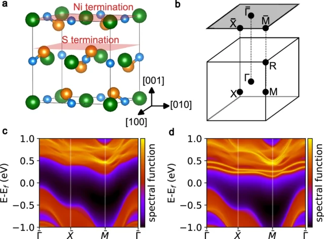
A scanning tunnelling microscope (STM) works by bringing an extremely sharp needle close enough to a surface that electrons can leak across the gap between tip and sample. Measuring that leakage at different energies reveals both the surface’s shape and how easily electrons can enter or leave it. In NiS₂, these measurements uncovered electronic states concentrated tightly along the step edges: the states extend for a long distance parallel to a step but stay confined to roughly one to two nanometres across it. In other words, the electrons are effectively free to move in one direction while remaining trapped in the other two, forming genuine one-dimensional conduction channels.
Surface spectra of the terminations observed in STM. Source: M. Iraola, H. Guo et al (2026) Nature Communications doi: 10.1038/s41467-026-76126-x
Two distinct kinds of surface step were observed, depending on whether the outermost atomic layer exposes nickel or sulfur atoms. Both carry electronic states associated with their steps, but they are not equally important. The nickel-terminated steps host states that sit right at the energy where electrical conduction happens, making them the most likely explanation for the surface conductivity that transport experiments had measured for years. The sulfur-terminated steps also host states inside the insulating gap, but their energy is positioned further away, making them less directly responsible for carrying current.
The study also tested what happens when a magnetic field is applied perpendicular to the surface. The step-edge states survived fields as strong as 10 tesla, a field far stronger than any produced by a laboratory magnet used for everyday purposes. Their intensity weakened somewhat, particularly on the sulfur-terminated steps, but the states were never destroyed. This robustness matters because NiS₂ already displays complicated magnetic behaviour of its own, which might easily have disrupted a more fragile conducting state.
The deeper explanation lies in how electrons are distributed inside the crystal. In an ordinary insulator, the occupied electronic states can usually be pictured as clouds centred on the atoms themselves. NiS₂ is different: calculations show that part of its electron density is naturally centred at special positions between atoms, specifically near the midpoints of pairs of sulfur atoms, where no atom actually sits. Physicists call these obstructed charge centres, and materials built around them belong to a class known as obstructed atomic insulators, a concept that grew out of a broader effort over the past decade to classify materials by the geometry, and not just the energy, of their electron states.
The concept of obstructed atomic insulator. In an OAI, the valence bands are induced from Wannier functions localized at obstructed Wannier charge centers (OWCCs)—symmetric positions in the crystal not occupied by any ion. Wannier functions are the localized molecular orbitals of crystalline systems. Source: M. Iraola, H. Guo et al (2026) Nature Communications doi: 10.1038/s41467-026-76126-x
Not ordinary metallic defects
This arrangement is not a chemical accident; it is protected by the symmetry of the crystal. When the crystal is cut to form a surface, though, the special positions that hosted this electron density can no longer fit together the way they did in the bulk. At a step edge, this mismatch creates what is known as a filling anomaly: an imbalance in how the available electronic states can be occupied, which leaves behind a state inside the insulating gap, localized right at the edge. Calculations of artificial step structures reproduce the main features seen under the microscope, including this localization, supporting the idea that the conducting channels are not ordinary metallic defects caused by broken chemical bonds, but a direct consequence of the crystal’s underlying electronic geometry.
The study also settles a long-standing question about NiS₂’s magnetism at low temperature. Below about 39 kelvin, the nickel magnetic moments arrange themselves into a non-collinear antiferromagnetic pattern, with neighbouring moments pointing in different directions that largely cancel out. Below about 30 kelvin, they rearrange again into a state that produces a small but measurable net magnetization. New neutron-diffraction measurements support a revised model of this low-temperature arrangement, resolving a debate about the material’s magnetic ground state that had lasted for roughly fifty years.
Taken together, the results give NiS₂ a significance well beyond its peculiar conducting surface. The material shows that strong repulsion between electrons, magnetism, and the geometry of electronic states can coexist within a single crystal. Such geometric protection is normally associated with topological materials, in which certain electronic states are shielded from disorder or defects by the crystal’s symmetry. The new results suggest that this protection can survive even when strong interactions push a material into being an insulator, making NiS₂ a rare setting for studying how the quantum-mechanical arrangement of electrons decides where electricity is allowed to flow within an otherwise insulating crystal.
Author: César Tomé López is a science writer and the editor of Mapping Ignorance
Disclaimer: Parts of this article may have been copied verbatim or almost verbatim from the referenced research paper/s.
References
Mikel Iraola, Haojie Guo, Fabio Orlandi, Sebastian Klemenz, Martina O. Soldini, Sandra Sajan, Pascal Manuel, Jeroen van den Brink, Titus Neupert, Miguel M. Ugeda, Leslie M. Schoop & Maia G. Vergniory (2026) One-dimensional conduction channels in the correlated Mott NiS2 arising from obstructed Wannier charges Nature Communications doi: 10.1038/s41467-026-76126-x↩
Topological quantum materials combine unusual electronic states with properties such as magnetism or superconductivity, offering possibilities for future electronics and quantum technologies. Researchers at Tohoku University have now shown that changing the number of layers in a crystal can provide a systematic way to design topological magnets. The work is published in the Journal of the American Chemical Society.
Topological quantum materials combine unusual electronic states with properties such as magnetism or superconductivity, offering possibilities for future electronics and quantum technologies. Researchers at Tohoku University have now shown that changing the number of layers in a crystal can provide a systematic way to design topological magnets. The work is published in the Journal of the American Chemical Society.
Material properties such as sound insulation, resistance to extreme heat and thermal expansion originate from how the zillions of microscopic building blocks (nuclei and electrons) interact at equilibrium and respond to perturbations. Atoms are typically about one ten-billionth of a meter across, so there can be a lot of parts to keep track of—a task that is complicated at the quantum-mechanical level, where particles are neither here nor there until observed.
Material properties such as sound insulation, resistance to extreme heat and thermal expansion originate from how the zillions of microscopic building blocks (nuclei and electrons) interact at equilibrium and respond to perturbations. Atoms are typically about one ten-billionth of a meter across, so there can be a lot of parts to keep track of—a task that is complicated at the quantum-mechanical level, where particles are neither here nor there until observed.
Researchers at Nagoya University have built a graphene nanoribbon that can switch which way it twists using a natural solvent. Graphene nanoribbons are thin ribbon-shaped structures made of fused carbon rings. Twisted or helical versions of these ribbons show promise for advanced light and electronic devices. However, no graphene nanoribbon could switch that twist on demand, until now.
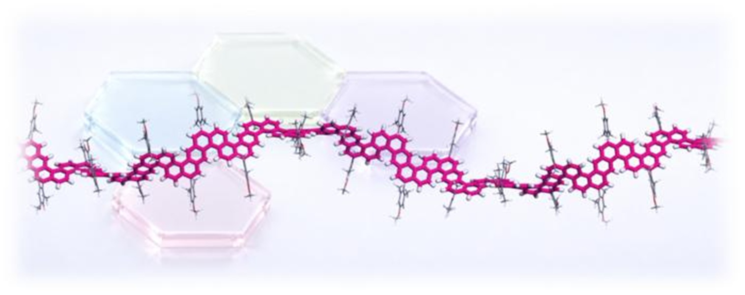
A 3D illustration of the [4]helicene nanoribbon shows the long chain of fused rings that gives the molecule its twisted structure. Source: Tomoyuki Ikai / Nagoya UniversityScientists have worked out how to switch between a right-handed and left-handed twist (chirality) by changing the solvent around it. The discovery 1 opens opportunities for new optical switches, chemical sensors, and spintronic components that adapt to changing environments.
Tomoyuki Ikai, lead author and professor at Nagoya University’s Graduate School of Engineering, is a polymer chemist inspired by natural helical structures such as DNA and proteins. Polymers are large molecules built from many small, repeating units linked together in a chain. Ikai had been working on ladder polymers, where each repeating unit is locked into place and cannot freely rotate around the bond connecting to its neighbor (unlike a typical flexible linear polymer).
“We used the same fusion approach already used to make predictable helical ladder polymers. But instead of a stable building block, such as [6]helicene, we used [4]helicene, a 4-ring unit written off as too unstable to be useful,” Ikai said.
Soak, twist, repeat
These units are difficult to control on their own because they switch their chirality too fast to hold one handedness. The team’s method fuses these small, restless units into one long chain. Once joined, they found that a neighbor effect took hold: each unit’s twist began to match its neighbors, and long stretches of the ribbon settled into a single, shared spiral.
To lock it in one overall direction, the researchers dissolved the ribbon in a natural chiral liquid, a liquid made of molecules that come in two mirror-image versions. They tested six candidates before they found the right one: beta-pinene, a compound found in pine trees and citrus peel.
Because beta-pinene molecules can be arranged in left- and right-hand mirror-images, these two versions each push the ribbon toward the opposite spiral. This also changed the twist direction of light the ribbon gave off, a property called circularly polarized luminescence, and is the first graphene nanoribbon shown to switch its light this way.
The switching induced a remarkably high degree of helical bias, with almost all of the helicene units aligning in the same direction. The switching effect is strongest at –90°C and grows weaker as the temperature rises toward room temperature.
“For a long time, people saw [4]helicene as unsuitable for chiral materials, because it could not be controlled,” Ikai said. “In this paper, we show that once you link enough of these units together, the instability itself becomes the useful part.”
A chiral solvent’s nudge toward one handedness is usually very weak on its own. Here, the ribbon’s own structure, with each unit mechanically linked to its neighbors, amplifies that weak nudge into a strong, nearly one-handed result.
An adaptive material
The researchers point to several possible future uses: The switchable light could serve optical devices. The ribbon’s chemical sensitivity to beta-pinene suggests it may work as a chiral sensor, and a similar design could one day help detect hazardous or unstable chemicals. Because graphene conducts electricity well, the ribbon may also suit electronic sensors.
The molecule’s twisted shape connects to spintronics, a field that uses the spin of electrons rather than just their charge. Ikai noted that a right-handed or left-handed structure can, in principle, let electrons of one spin pass through more easily than the other, a property helical structures are known for in physics literature.
The current design only holds its twist while it stays in the chiral liquid. If the solvent is removed, the ribbon drifts back to a mixed, unstable state. Ikai’s next goal is a form of “chiral memory,” a way for the ribbon to lock in its twist even after the solvent is gone. This next step builds on memory techniques the researchers have explored in other helical systems and is now applied to graphene for the first time.
References
Ikai, T., Inagaki, H., Oki, K. et al. (2026) Dynamic helical poly[4]helicene nanoribbon. Nat Commun doi: 10.1038/s41467-026-76724-9↩
Water droplets sliding across solid surfaces can acquire electric potentials of thousands of volts and thereby corrode non-conductive surfaces on metals when they discharge. That is the conclusion of researchers in Germany who say that the poorly-understood phenomenon warrants further investigation to help prevent corrosion of vulnerable outdoor equipment and cultural heritage sites.
Metal corrosion by water droplets is a serious economic and safety issue, and prevention begins with the proper understanding of the relevant processes. Conventional wisdom is that most corrosion is caused by a combination of physical abrasion by the motion of the droplets and chemical degradation from natural acids and anthropogenic pollutants in the water. The notion that electrochemistry might play a significant role in corrosion had not been seriously considered, says physical chemist Hans-Jürgen Butt of the Max Planck Institute for Polymer Research in Mainz.
Part of the reason, he believes, is that, until relatively recently, it was thought that the triboelectric effect (electrically charging objects by rubbing them together) did not work in liquids. “If you have a solid and you rub another insulating solid against it you get electron transfer – I think this has been known for more than 2500 years” he says. However, this relies on atomic-scale roughness of the surface to concentrate charge at specific points where bonds can be broken – and fluids cannot, by definition, be rough.
“If you take a water droplet and let it slide there is some mechanical force from surface tension, but that’s much too low,” says Butt. “There is no way you could generate enough energy locally to pick up an electron or to put an electron or an ion from the water onto the surface.” In the past 10 years, however, it has become increasingly clear that sliding droplets do become highly charged.
Sloping surfaces
In their present work Butt and colleagues deposited water droplets onto copper surfaces covered with 60 nm of Teflon. When they dropped droplets straight onto the surface, they observed no corrosion. They then deposited droplets first onto a variety of other sloped insulating surfaces such as plant leaves, PVC construction boards and the perfluorooctadecyltrichlorosilane (PFOTS) hydrophobic coating often used on window glass. The droplets ran down these surfaces and then fell onto the Teflon-coated copper. After around 3000 droplet impacts, atomic force microscopy and confocal microscopy revealed evidence that the droplets had corroded both the coating and the underlying copper.
The researchers believe that the droplets become positively charged as they slide down the sloping surface. As they fall onto the coating, the potential difference between the copper and the underlying copper can exceed 1 kV. This is greater than the dielectric breakdown strength of the coating, causing the droplet to discharge. This damages the coating and leaves the underlying metal vulnerable to further oxidation.
To test their hypothesis, the researchers measured charge movement within the copper surface, showing that negative charge flowed towards droplets dripping off insulating surfaces. They also used high-speed cameras to show that, whereas a drop deposited directly retained its spherical shape before impact, a dripping drop was drawn into a cone shape, producing a tip of positive charge that would increase its corrosive capacity.
Uncertain consequences
The practical implications of this are unclear. “Technical coatings on cars, ships etc. are typically 100 microns and thicker, so the process we describe is probably not of direct relevance,”says Butt. However, the phenomenon could be involved in the degradation of monuments and other outdoor historical objects. “We have evidence that surfaces change their properties when you slide charges over them, but the real consequences are not yet known,” explains Butt.
He says his own group is most clearly focused on understanding the fundamental physics involved. “We still don’t know why the heck there is such a charge separation: it’s energetically unfavourable, it should not happen, but it happens.” he says. “The one effect we describe here is, in a way, pretty trivial – everyone knows that if you have a high potential and it’s somehow grounded there is a breakthrough – but what happens at the surface with this deposited charge is not clear.”
Materials scientist Zhong Lin Wang of Georgia Institute of Technology in Atlanta was one of the first researchers to discover the triboelectric effect in liquids, and helped to develop the triboelectric nanogenerator used to quantify it. “The transferred electrons can be kicked back to the water solution, resulting in chemical reaction at the vicinity surface. This process, called contact-electro-catalysis, was first proposed in 2022, and is now an active field of research in chemistry, materials and environmental science.” He says. “[Butt and colleagues] show that the electrons transferred from the water droplet can ‘break’ the surface coating layer and lead to local oxidation. This is an interesting discovery.”
Fusion reactors, devices that generate energy by fusing light atomic nuclei at extremely high temperatures, could contribute to ongoing efforts aimed at producing electricity more sustainably. The extreme environment inside these devices, however, can damage materials that surround the superheated, electrically charged plasma where the nuclear fusion reaction takes place.
Every electronic and optoelectronic device generates heat, and today that heat is managed almost entirely from the outside. Heatsinks, fans, cold plates and refrigerators are bulky exterior measures bolted onto a chip or package after the fact. They treat heat as a single averaged quantity to be removed in bulk, even though the heat is actually produced locally, component by component, deep inside the circuitry.
In January 2024, physicists at TU Dortmund University demonstrated a continuous time crystal in a semiconductor whose oscillations remained stable for hours. In a new study published in Nature Communications, Professor Alex Greilich and his team show that many such time crystals can form in the same material and synchronize their electron-nuclear spin oscillations.
Over the last decade, researchers have developed two-dimensional materials with fascinating quantum effects that could be harnessed for next-generation technologies.
Scientists in China predict that stacking two microscopic layers of boron could set a new record for superconductivity. Superconductors are materials that conduct electricity with zero resistance. Traditional types need temperatures close to absolute zero to work, requiring complex and expensive cooling equipment.
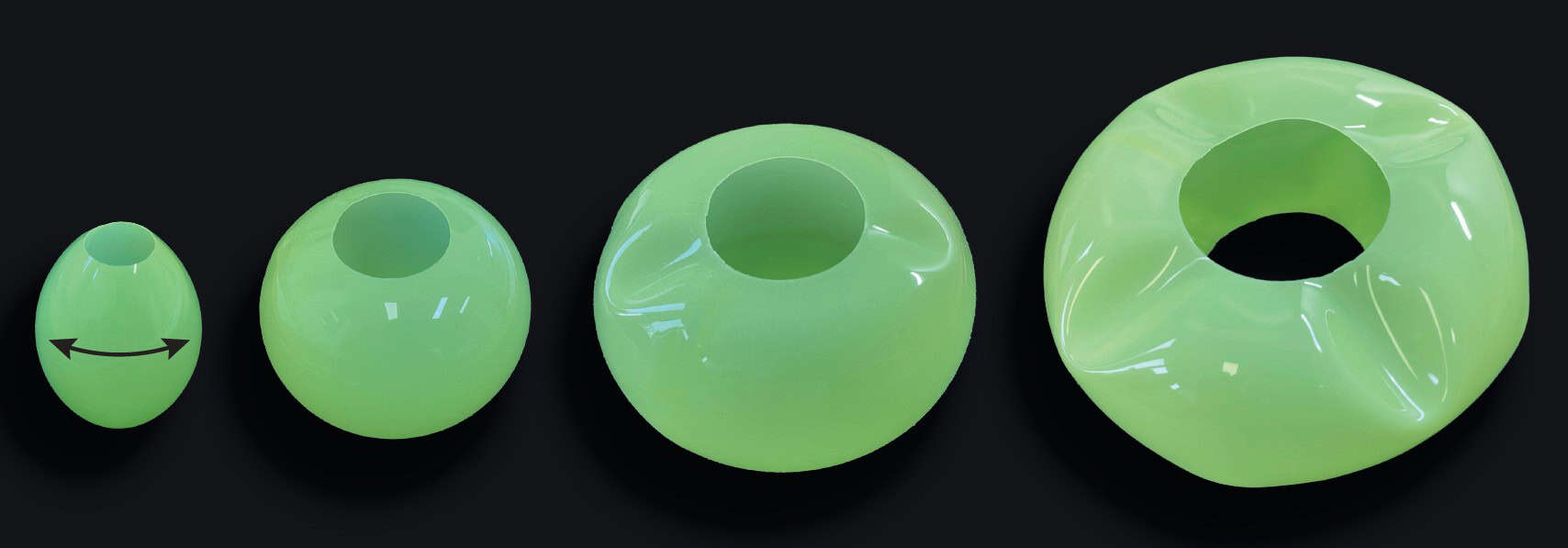
More dimples A series of hollow objects made from elastic sheets. The size of the objects increases in the directions indicated by the arrows. The number of buckles in the object is seen to increase as its shape changes. (Courtesy: Yafei Zhang)
A new mechanism governing the geometric shapes of growing elastic sheets has been identified by a trio of physicists in Israel. Through a combination of simulations and experiments, Eran Sharon and colleagues at the Hebrew University of Jerusalem showed that the dimpled patterns that form in a growing elastic object have topological origins.
This mechanism is unrelated to geometric incompatibilities, which are known to dimple natural materials. The discovery could lead to a deeper understanding of how complex shapes emerge in the natural world – and to the development of new artificial materials.
Thin sheets are ubiquitous in nature: examples include leaves, petals, and the cellular linings of organs and blood vessels. The complex makeup of natural sheets means that local regions within them have preferred mechanical rest states that are incompatible with those of other regions. As a result, there is no way to arrange the sheet so that every part is simultaneously stress free – leading to effects like wrinkling, bending, and buckling.
Called geometric incompatibility, this phenomenon is responsible for numerous geometric forms in the natural world, enabling growing tissues to shape themselves without any external influence. For some time, researchers have attempted to mimic these natural mechanisms in synthetic materials.
Richness of shapes
“Looking at natural growth processes, as in plants growth, or embryo development, we see amazing richness of shapes and shape development that currently cannot be achieved with conventional fabrication methods,” says Sharon.
Sharon’s group has already shown that many patterns in nature can be understood in terms of the Gauss and Mainardi-Codazzi-Peterson incompatibilities – which were developed in the 19th century. Together with team member Michael Moshe, whose group explores the interplay between mechanics and geometry in soft materials, their work led to discoveries including the mechanical origins of shape selection in rose petals.
Now, Moshe and Sharon have teamed-up with Yafei Zhang to identify a phenomenon that cannot be explained by those mechanical instabilities. In their experiment, they started with a uniform elastic sheet formed into a hollow sphere, with circular holes at each pole. When they added wedges of material into the sheet to mimic growth, it initially behaved like a smooth, growing sphere – but only up to a certain point.
Missing mechanism
“The growing sheet satisfies the established local compatibility conditions, and is thus expected to show smooth ‘boring’ shape,” Moshe explains. “Yet it unexpectedly, develops a crumpled appearance, suggesting that an important shaping mechanism was missing from the existing framework.”
Important clues came when the team cut into the crumpled sphere along a meridian, from pole to pole. Instantly, the crumpling disappeared, and the sphere relaxed back to its original smooth shape. This effect also occurs in simulations of a smoothly growing sphere.
With no changes to the Gauss or Mainardi-Codazzi-Peterson incompatibilities governing the mechanical forces in the sheet, the trio concluded that the sudden transformation emerged from an entirely different mechanism, rooted in the mathematical principles of topology. In this view, unlike smooth geometric transformations such as bending, stretching, or twisting, which preserve a shape’s mechanical properties, cutting introduces a sudden transformation that changes its mechanical behaviour.
In this way, the meridional cut brought the sphere into a new topological state. “Unlike conventional incompatibility, this frustration is topological in character, and can be quantified by a global measure,” Moshe explains. “It provides a new mechanism by which growing sheets can select complex, wrinkled or dimpled shapes.”
The trio’s discovery now raises new mathematical questions about the limits of growing elastic sheets, beyond which their smooth geometries can no longer be maintained. “What we have discovered that the geometrical principles we knew before should be supplemented with topological considerations, leading to an even wider class of shaping principles,” Sharon says. “This allows a better understanding of morphogenetic processes and expands our abilities to shape synthetic structures.”
In turn, the team’s insights could uncover new understanding of how shaping mechanisms could be harnessed, perhaps leading to the discovery of new metamaterials, with shapes and mechanical functions programmed into their growth.
Ruthenium dioxide (RuO2) is a metal oxide that commonly serves as an important metallic conductor, quantum material and industrial electrocatalyst. While there have been debates surrounding the magnetic properties of RuO2, it is generally thought to be nonmagnetic in its bulk form. But now, a new study, published in Science Advances, has found that very thin layers of RuO2 can become magnetic when its lattice is placed under strain.
One of the most striking discoveries in condensed matter physics over the past few years is that simply rotating one atomically thin crystal on top of an identical layer can create entirely new electronic behavior. This idea became famous in 2018, when physicists found that graphene sheets stacked at a very particular “magic angle” could turn into a superconductor, even though a single sheet of graphene is not. That discovery launched an entire field, sometimes called twistronics, built around moiré patterns: the large-scale interference patterns that appear when two crystal lattices are laid on top of each other with a slight mismatch in angle or spacing. In many materials, these patterns reshape how electrons move, sometimes producing superconductivity or other exotic collective states.
Moiré collapse
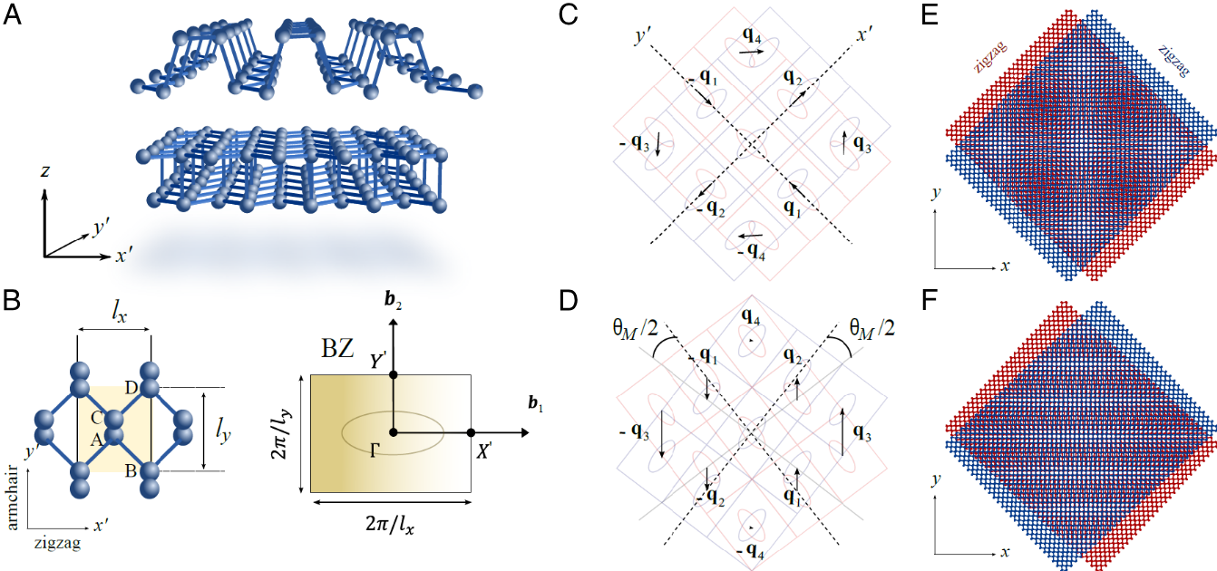
Most of this research has focused on materials whose crystal structure looks roughly the same in every direction, such as graphene, where the interesting physics shows up only at very small twist angles, close to perfect alignment. Now, a team of researchers instead looks at a strongly directional material: bilayer black phosphorus, whose atomic structure behaves very differently along two perpendicular directions in the plane, somewhat like a fabric that stretches easily one way but not the other. That built-in directionality turns out to change the whole logic of moiré physics, producing an effect the authors call moiré collapse. 1
Moiré collapse in twisted anisotropic homobilayers. Source: D. J. P. de Sousa et al. (2026) Proc. Natl. Acad. Sci. U. S. A. doi: 10.1073/pnas.2527371123 / fair use
In black phosphorus, the two layers start out rotated 90 degrees relative to each other. As that angle is dialed away from 90 degrees, the moiré pattern does something unusual. Rather than staying a two-dimensional pattern, like a slowly shifting checkerboard, it stretches more and more along one direction until, at a specific angle that depends only on the material’s own geometry, it effectively stops repeating in the other direction altogether. What remains behaves like a one-dimensional crystal, even though the material is still built from ordinary two-dimensional atomic sheets. For twisted bilayer black phosphorus, the calculations place this collapse at a twist of about 71.6 degrees, or equivalently about 18.4 degrees away from the initial 90-degree arrangement.
Pure geometry
This transformation has nothing to do with how electrons repel or attract each other; it is pure geometry. The mathematical description of the moiré pattern, expressed in terms of the directions in which its periodicity repeats, is squeezed from two independent directions down to one. In ordinary space, this means the pattern keeps a well-defined repeat distance along one axis while stretching out indefinitely along the other, with no repeating pattern left in that direction at all.
Such a dramatic structural change reshapes the electrons riding on top of it. At the untwisted 90-degree configuration, the anisotropy of one layer happens to cancel out the anisotropy of the other, so electrons move about equally well in every in-plane direction. As the twist angle approaches the collapse point, that cancellation breaks down. The electron energy bands become sharply directional, and electrons increasingly travel along one preferred line rather than spreading across the plane. Their energy spectrum starts to show the telltale fingerprints of one-dimensional systems, including sharp spikes in the density of available electron states known as one-dimensional van Hove singularities.
Luttinger liquid physics
One-dimensional conductors behave very differently from ordinary metals. In a three-dimensional metal, electrons can mostly be treated as independent particles that only weakly notice one another. Confine them to a single dimension, however, and that picture stops working: electrons cannot slip past each other, so they are forced to move collectively, in a coordinated wave-like fashion. The framework that describes this collective behavior, called Luttinger liquid theory, traces back to work by Sin-Itiro Tomonaga in 1950 and Joaquin Luttinger in 1963, and it has since been confirmed experimentally in systems such as carbon nanotubes. In a Luttinger liquid, the basic excitations are not single electrons at all, but collective ripples of charge and spin, and this leads to electrical transport properties that look qualitatively different from those of a normal metal.
The calculations in this study show that moiré collapse naturally sets up the conditions Luttinger liquid physics requires. As the collapse angle is approached, the one-dimensional electronic channels that form become progressively less coupled to their neighbors, making the correlated, wave-like behavior increasingly favorable. The analysis estimates a Luttinger parameter of about 0.3 for the collapsed black phosphorus system, a value indicating strong electron-electron interactions, and it predicts distinctive collective charge oscillations and unusual, non-metallic patterns in electrical conduction that could, in principle, be measured in the laboratory.
A notable feature of this mechanism is that the electron bands stay quite dispersive even at collapse, with electron speeds exceeding 100 kilometers per second. This sets it apart from most previously studied moiré systems, including twisted graphene, where strong correlations usually arise because the electronic bands become extremely flat and electrons effectively slow to a crawl. Here, the correlated behavior instead comes from the geometric collapse of the moiré lattice itself, with fast-moving electrons confined to one dimension rather than slow ones spread over two.
Moiré collapse is not a peculiarity of one material
To test these ideas, the researchers combined simplified mathematical models with detailed first-principles calculations of the atomic and electronic structure. Beyond black phosphorus, they found the same collapse in twisted bilayer tin selenide, another layered material with strongly directional bonding. The details of the electronic structure differ somewhat because of the specific atomic orbitals involved, but the same geometric collapse into quasi-one-dimensional channels appears, suggesting the phenomenon is not a peculiarity of one material but a general consequence of twisting any sufficiently anisotropic crystal.
Taken together, the findings outline a different strategy for engineering exotic quantum matter. Instead of hunting for a special magic angle that flattens electronic bands, as in twisted graphene, this approach relies on a purely geometric collapse angle at which a two-dimensional moiré material naturally turns one-dimensional. If confirmed in experiments, it would offer a new and versatile platform for studying Luttinger liquids and other correlated electronic phases that only emerge when electrons are squeezed into moving along a single line.
Author: César Tomé López is a science writer and the editor of Mapping Ignorance
Disclaimer: Parts of this article may have been copied verbatim or almost verbatim from the referenced research paper/s.
References
D. J. P. de Sousa, S. Lee, F. Guinea, and T. Low (2026) Moiré collapse and Luttinger liquids in twisted anisotropic homobilayers Proc. Natl. Acad. Sci. U. S. A. doi: 10.1073/pnas.2527371123↩
Many of today’s electronic devices — from the semiconductors in your cell phone to the photovoltaic cells in your solar panels — are built on thin-film substrates. The thin film is an electronically conductive material while the substrate is an inert material. Or is it?
Physicists and materials scientists have long assumed substrates do not react to electrical stimulus, but new research from the University of California San Diego Alex Frañó’s lab and a team of collaborators has shown that substrates are not inert after all. The discovery 1 has the potential to help engineers build the dense, three-dimensional, brain-inspired computer chips needed for more energy-efficient computing.
Source: Unsplash
In a human brain, a vast network of neurons works across different regions, enabling every thought and action we take. Yet thoughts that are quick and simple for humans — recognizing faces, differentiating a cat from a dog or solving a captcha — can be devilishly hard and energy-intensive for computers. Quantum materials may provide a solution.
It was this quest to develop new materials that led Frañó’s lab to study vanadium dioxide thin-film devices. When a voltage is applied to the thin film, an electric filament forms — something similar happens when the Earth and atmosphere create a voltage strong enough to result in lightning. The filament in the thin film drives the device’s electrical spiking, much like the signals in our neurons.
This reaction has been studied countless times in labs around the world, but Frañó’s lab was implementing a new technique, developed by graduate student Elliot Kisiel, called dark-field X-ray microscopy. Kisiel, who spent most of his graduate studies at Argonne National Laboratory and is now a Mayer Postdoctoral Fellow there, developed the tool to combine the best of two worlds: electron microscopy and X-ray diffraction.
“Dark-field X-ray microscopy gives us the ability to look at an entire device in one image, which not only greatly improves how fast we can perform these measurements, but also allows us to study the areas surrounding the devices with high fidelity,” he stated.
A changing substrate
Since the lenses for X-rays are often thick and, therefore, absorb most of the X-rays that pass through them, the team needed to look at something that provided more signal, which is why they decided to look at the substrate during some of their preliminary testing with this new technique.
What they saw was completely unexpected: not only was there a change in the thin film, but there was also a change in the substrate, showing for the first time that the two parts were sharing energy or “coupled.” This discovery went against everything scientists had assumed about substrates for decades.
Materials for a new age of computing
Thin films are so called because they are vanishingly thin — around 100 nanometers — while the substrates they sit on can be 10,000 times thicker. Despite their lopsided sizes, in this experiment, the thin film was able to push and pull on the substrate. Frañó likened the discovery to a tree on a mountaintop being able to move the entire mountain. Furthermore, the substrate also acted on the thin film, each pushing and pulling on the other.
They spent the next four years making sure what they saw wasn’t a fluke. They not only reproduced the results doing the research exactly as they had done it the first time, but they also reproduced the results when they changed certain aspects of the sample, such as the thickness and material of the substrate. They also tested their results using different instrumentation. Much of that work was done at Argonne, which has a synchrotron facility that produces high brilliance X-rays, and at Brookhaven National Laboratory, home to the world’s only all-electric ultrafast electron microscope, which is able to capture exactly how a working device behaves under realistic operating conditions.
It wasn’t a fluke.
“The assumption that substrates are inert needs to be rethought,” Frañó stated. “Going forward, we have to assume that the substrate is undergoing changes when the film is. This is a transformational notion that counters decades of previous supposition.”
This paper is a companion to a paper that was published last year in ACS Nano2. In that paper, they used dark-field X-ray microscopy to study the thin film, while this paper focuses on the substrate. Together they illustrate how one research result leads to the next research inquiry.
In Frañó’s case, the question he now asks himself is, “What can we do with this new substrate discovery? If a tree is moving the whole mountain, let’s find a way to capitalize on that.”
One idea is that the substrate can act as a medium that can couple materials on either end of the substrate. Currently, thin film devices are connected two-dimensionally, but if researchers could build on both sides of a substrate, it would allow for three-dimensionality, opening up the possibility of denser, more interconnected computer chips, and bringing us one step closer to the next generation of computing.
References
Elliot Kisiel et al. (2026) Dynamic asymmetric strain imprinted into substrates by an oxide thin film doi:10.1126/science.adt9347↩
Elliot Kisiel et al. (2025) High-Resolution Full-Field Structural Microscopy of the Voltage-Induced Filament Formation in VO2-Based Neuromorphic Devices. ACS Nano doi: 10.1021/acsnano.4c14696↩
Static electricity is one of those everyday phenomena that turns out to be much more complicated than you might expect. Indeed, our guest in this episode of the Physics World Weekly podcast has devoted much of his career to understanding how objects exchange electrical charge – a process that he says scientists are mostly “clueless” about.
Based at the Institute of Science and Technology Austria, Scott Waitukaitis is in conversation with Physics World’s Margaret Harris. He explains how his early work in granular physics opened his eyes to the many unsolved problems related to static electricity. They also chat about some of Waitukaitis’s current research projects including his quest to understand the role that adsorbed molecules play in how an object is charged.

 Login