Login

Siemens EDA Says AI Can Cut Chip Design Time by Up to 10x
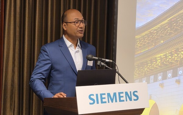
Siemens EDA outlined how artificial intelligence (AI) can reduce semiconductor design time by as much as tenfold, highlighting multi-agent AI as a key technology for addressing the growing complexity of chip development.
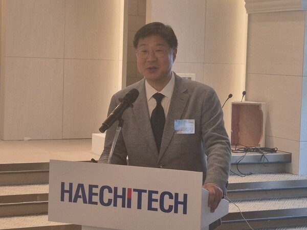
Ankur Gupta, Senior Vice President of IC Products at Siemens Digital Industries Software's Electronic Design Automation (EDA) business, presented the company's AI-native design strategy during a media briefing held at Lotte Hotel World in Seoul on Aug. 11.
"Last month, we integrated a broad range of agentic AI capabilities into our EDA platform, including multi-agent workflows, self-verification and long-duration autonomous execution," Gupta said.
Multi-agent AI enables multiple AI agents to divide and coordinate semiconductor design tasks. After engineers specify design parameters such as manufacturing process, voltage and temperature conditions, the agents automatically perform verification, debugging and design modifications. Siemens introduced its AI-powered EDA system, Fuse, in 2025.
According to the company, multi-agent AI can accelerate transistor characterization workloads by up to ten times while reducing token costs by roughly 90%.
"Engineers at large companies are restricting or even suspending the use of large language models because token budgets have become unsustainably high," Gupta said. "The EDA industry recognizes this as a critical challenge and is developing technologies that deliver much higher token efficiency."
Siemens is also collaborating with Nvidia to develop AI-enabled EDA tools. Earlier this year, the two companies announced a strategic AI partnership aimed at integrating AI throughout the semiconductor design flow—from register-transfer level (RTL) design through verification. Under the collaboration, Nvidia's AI infrastructure and Nemotron models will be incorporated into Siemens' EDA software.
Gupta said modern semiconductor designs are reaching unprecedented levels of complexity.
"Today's chips contain more than 200 billion transistors and exceed thermal densities of 100 watts per square centimeter," he said. "Conventional design approaches can no longer keep pace with the speed of the market."
He added that even modest improvements in chip efficiency can have a substantial impact.
"A 5% reduction in power consumption translates into significant energy savings at the system level, making it an important factor in building a more sustainable industry," he said.
Other leading EDA vendors, including Synopsys and Cadence Design Systems, are also incorporating AI capabilities into their design platforms.
Gupta said Siemens differentiates itself through its focus on design verification, emphasizing that the company provides a comprehensive integrity platform.
"In semiconductor design, a single minor error can result in design failure or lower manufacturing yields," he said. "Because such failures can cost hundreds of millions of dollars, building software that customers can trust is the industry's highest priority."
Siemens also said AI can significantly reduce verification time, one of the most time-consuming stages of semiconductor development. According to the company, its EDA tools can accelerate automatic test pattern generation (ATPG) simulation by up to five times for certain workloads. ATPG simulation is used to validate test patterns in virtual environments before they are applied to detect manufacturing defects in semiconductor devices.