
❌

Reading view

Encapsulation enhances surface structure imaging of 2D quantum material
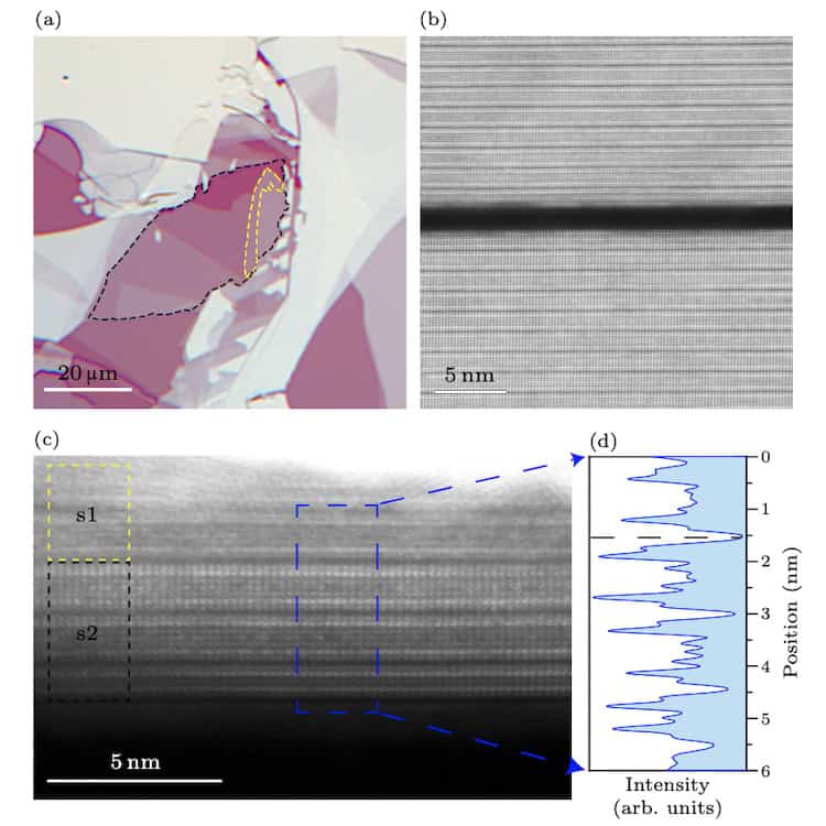
Preserving MBT’s septuple-layer surface
Surface preservation (a) Optical image of MBT-on-MBT sample, with the capping flake s1 and target flake s2 outlined in yellow and black, respectively. (b) TEM image of a homojunction interface with a thick capping layer, showing a substantial interface gap. (c) TEM image of an optimized interface using a thin capping flake s1 on the target s2. (d) The intensity profile extracted from the blue dashed box confirms that both the bottom surface of s1 and the top surface of s2 maintain a distinct seven-atom septuple-layer structure, demonstrating effective surface preservation. (Courtesy: Luo et al., Chin. Phys. Lett. 43 050713)

Thanks to a novel encapsulation technique, researchers at Fudan University in Shanghai, China, have succeeded in imaging the surface structure of the atomically thin topological quantum material MnBi2Te4 (MBT) for the first time. The work could help advance our understanding of the intrinsic properties of this technologically important class of materials and enable their use in novel devices.

The electronic, magnetic and topological properties of materials thinned down to atomic-scale thicknesses are very different to those of their bulk counterparts. They can, for example, be employed to study exotic quantum states that could prove useful for a host of advanced applications, such as next-generation spintronics and dissipationless electronics.

Before such devices see the light of day, however, we need to understand these emergent properties, which means accurately determining the surface atomic structure of these materials. This is no easy task because these surface structures are extremely sensitive to their environment. What is more, the most common technique used to study them, transmission electron microscopy (TEM), requires samples to be prepared as lamellae, which degrades them, changing their structure. The high-energy electron irradiation beam in the microscope does them no good either.

In the new work, a team led by Yuanbo Zhang of the State Key Laboratory of Surface Physics and department of physics at Fudan University, studied the topological quantum material MBT. This is the only intrinsic magnetic topological insulator made in the laboratory so far and can be used to study novel topological states – such as the quantum anomalous Hall effect and axion-insulator physics – many of which are fundamentally governed by surface states.

MBT’s surface is exceptionally vulnerable

Like other sensitive 2D materials, explains study co-author Jingjing Gao, MBT’s surface is exceptionally vulnerable to external perturbations, such as ambient air exposure, heat or standard electron microscopy preparation. These degrade the surface layer and irreversibly alter its structure. Indeed, a previous TEM study also revealed that the septuple-layer structure of an MBT flake transforms into a Bi2Te3-like quintuple layer configuration under ambient conditions.

To overcome this problem, Gao and colleagues developed a protective encapsulation technique that successfully shields the delicate surface structure of MBT from its environment and protects it during TEM sample preparation.

The researchers examined two types of encapsulating materials. The first was hexagonal boron nitride (hBN), which is chemically inert and already routinely employed to protect 2D materials. The second was a thin flake of MBT itself, which provides  a “homomaterial” capping layer. They encapsulated the MBT in one of these two materials immediately after they had exfoliated (or shaved off) flakes of MBT from a bulk sample. They did this inside an inert argon-filled glovebox.

An atomic-scale barrier

The protective layer acts like an atomic-scale barrier that isolates the MBT surface from oxygen, moisture, ion-beam damage and other environmental disturbances produced during the focused-ion beam processing used to prepare the samples for TEM. It also protects the MBT from the high-energy electron irradiation in the imaging microscope.

The researchers found that the homomaterial encapsulation is especially protective because the atomically similar layers can intimately contact with a minimal interfacial gap.

The technique strongly reduces defect formation, so the original lattice structure remains stable throughout the entire TEM workflow, explains Gao. “We therefore succeeded in safeguarding the ‘true’ surface throughout, allowing us to visualize the intrinsic septuple-layer structure at atomic resolution for the first time.”

The work will be important for both understanding intrinsic magnetic topological insulators and for developing quantum devices from these materials in the future, she tells Physics World. “Making such devices will demand exceptionally stringent requirements for sample surface and interface quality. This is because the MBT’s unique topological and magnetic properties are hosted by its surface states and even minor atomic reconstruction can distort its intrinsic quantum behaviour.”

Looking ahead, the researchers, who detail their work in Chinese Physics Letters, say they will now be looking to construct heterostructure devices with high-quality intrinsic surfaces and interfaces based on MBT. They will also make use of their encapsulation strategy to fabricate and study magnetic topological heterostructures.

“We will also explore topological superconductivity by interfacing MBT with superconductors, thereby advancing the development of topological quantum computing platforms,” reveals Gao.

The post Encapsulation enhances surface structure imaging of 2D quantum material appeared first on Physics World.

  •  

Altermagnets can turn neighbouring materials altermagnetic, too

Altermagnets can transfer their unusual magnetic properties to nonmagnetic materials placed next to them, say theorists in China and the US. This so-called “proximity effect” had already been observed in ferromagnets and superconductors, but it is new for altermagnets, which were only recognized as a distinct class of magnetic materials in 2024. If confirmed experimentally, the team says the effect could aid the development of advanced quantum materials with applications in fields such as spintronics, valleytronics and fault-tolerant quantum computing.

In ferromagnets, proximity effects make it possible to tune properties such as magnetic anisotropy, coercivity and exchange bias in nonmagnetic materials that have acquired magnetic polarization from a neighbouring ferromagnet. Similarly, ordinary materials that have picked up superconducting correlations from a nearby superconductor are a mainstay of experiments on topological superconductivity and topological quantum computing.

In the latest research, physicists led by Tong Zhou of the Eastern Institute of Technology in Ningbo sought to understand whether altermagnets could likewise transfer their behaviour to a neighbouring material. To do this, they created a model of a van der Waals bilayer heterostructure in which the bottom layer is a two-dimensional (2D) altermagnet, V2Se2O, while the top layer is a non-magnetic semiconductor, PbO.

Zhou explains that the vanadium atoms in V2Se2O form two opposite-spin sublattices that are connected by rotational symmetry rather than by simple translation or inversion. This complex structure is what gives V2Se2O its characteristic altermagnetic spin splitting, with a band structure in which spin-up and spin-down electrons have different energies that vary in periodic patterns. V2Se2O also has a so-called spin texture, which is a pattern of spin polarization that produces a net zero magnetization in the material.

First-principles calculations

Using first-principles calculations, the researchers found that the distinctive symmetry-patterned magnetism of V₂Se₂O can indeed transfer into the PbO layer across the interface between them. As a result, Zhou says the originally spin-degenerate bands of PbO develop a clear momentum-dependent spin splitting.

Importantly, this pattern is not arbitrary. Instead, it follows the symmetry expected from the altermagnetic order of V2Se2O. What is more, the real-space spin density of the PbO mirrors the symmetry of the V2Se2O, showing that it has inherited altermagnetism rather than simply becoming generically spin polarized.

When the researchers rearranged the V2Se2O into a conventional antiferromagnetic configuration with no alternating spin splitting, they found that the induced splitting in PbO disappeared. They also observed that the degree of induced splitting decreases when the PbO is placed further away from the V2Se2O, confirming the proximity effect.

As a final piece of evidence, the researchers searched for similar proximity effects in other altermagnetic systems, ranging from insulators to metals and covering material platforms with 3D architectures as well as 2D ones. “Even graphene, one of the most common 2D materials, can acquire altermagnetic characteristics when interfaced with CrSb, which is an experimentally well-established altermagnet,” Zhou notes.

Altermagnets as interfacial “spin-pattern generators”

One of the work’s main implications is that altermagnets could be used to generate spin patterns in many otherwise non-magnetic materials, Zhou tells Physics World. “This means that instead of searching only for intrinsic altermagnets, we can now design ‘proximitized’ altermagnetic systems by combining an altermagnet with a semiconductor, metal or superconductor,” he says.

In semiconductors, Zhou notes, the altermagnetic proximity effect can induce controllable spin and valley splitting, which are promising for spintronics and valleytronics devices, respectively. In superconductors, meanwhile, the effect can generate momentum-dependent spin splitting without the need to apply an external magnetic field or introduce net magnetization – something that Zhou says offers a new route toward topological superconductivity and the Majorana modes that could revolutionize fault-tolerant quantum computing. “More generally, this effect provides a versatile platform for designing field-free spin devices, topological quantum devices and multifunctional van der Waals heterostructures,” he says.

Looking ahead, Zhou and colleagues say they would now like to observe the altermagnetic proximity effect in heterostructures fabricated in the laboratory. They also want to find out how to control the strength of the effect – for example, by changing interlayer spacing, stacking, strain, gating and possibly even layer twisting.

“More fundamentally, an important question is how fast and how reversibly altermagnetic order, and therefore the altermagnetic proximity effect, can be reconfigured dynamically,” Zhou says. “That would be especially interesting for controlling spin-dependent transport and topological phases in real time.”

The research is described in  Physical Review Letters.

The post Altermagnets can turn neighbouring materials altermagnetic, too appeared first on Physics World.

  •  
❌