Static electricity is one of those everyday phenomena that turns out to be much more complicated than you might expect. Indeed, our guest in this episode of the Physics World Weekly podcast has devoted much of his career to understanding how objects exchange electrical charge – a process that he says scientists are mostly “clueless” about.
Based at the Institute of Science and Technology Austria, Scott Waitukaitis is in conversation with Physics World’s Margaret Harris. He explains how his early work in granular physics opened his eyes to the many unsolved problems related to static electricity. They also chat about some of Waitukaitis’s current research projects including his quest to understand the role that adsorbed molecules play in how an object is charged.
Researchers at the University of Michigan have created a device that enables them to control the flow of electrons through a semiconductor using only laser light—no electrical power source required.
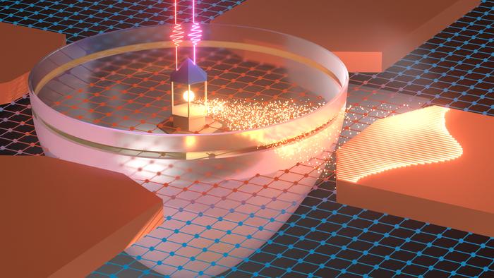
When two pulses of different colored lasers (the two waves at the top of the image) light meet in a new device created at the University of Michigan, researchers create a beam of electrons (small golden particles) that flows in a controllable direction. By changing the laser colors, the electron beam can sweep through different directions like the beam of a lighthouse. Illustration: Yiming Gong
This device was built 1 to explore fundamental physics and realize a previously unobserved behavior, but it could also open doors for new applications in areas that bridge optics and electronics, including sensing, imaging and telecommunications. The phenomenon could help improve how signals are sent through and between devices, as well as create new opportunities to store more information in those signals.
“This electrical device that we manufactured at the Lurie Nanofabrication Facility has the potential to turn into something that measures different aspects of light,” said Yiming Gong, who helped lead the project as a doctoral student in the U-M Department of Physics. “But this originates from a very fundamental level of physics, which is the interference between different optical absorption processes.”
The researchers showed they could induce the orderly flow of electrons through a semiconductor using two different colors of light. By rotating the polarization of the two optical fields—the direction that the light waves wiggle—the researchers could also control the direction of the electronic current.
“This isn’t the way things normally work. When you think about electrons moving through a material, they’re moving because you’ve applied an electrical field and they actually bounce around and drift across the materials. Here, using light, you can actually sort of squirt the electrons in a specific direction without applying an electric field,” said U-M physicist Steven Cundiff, senior author of the team’s report.
Although previous work had shown the ability of light to get electrons flowing with light alone, this work goes a step further and shows the light gets electrons flowing in a narrow beam in a specific direction.
“The light no longer merely switches the current on; it also aims it,” Cundiff said.
Cundiff likens this to a lighthouse, which sweeps a beam of light by rotating its lamp. Here, the beam is made of electrons and that beam can be rotated by rotating the polarization of the two phase-coherent optical fields.
The phenomenon relies on quantum interference, which arises when two colors of light drive different absorption pathways to the same final state. The light transfers energy to the semiconductor material in discrete, or quantized, packets called photons, which mobilize the material’s electric charge carriers.
In the set-up, the incident light is absorbed by two routes at once, and the routes can be thought of as overlapping ripples, Cundiff said. Those ripples line up and enhance each other for electrons traveling a certain direction, but cancel each other out for electrons moving in other directions.
A collaborator on an earlier project, J.E. Sipe of the University of Toronto, had predicted it would be possible to create such an “electron lighthouse.” Now, working with the Lurie Nanofabrication Facility, Gong was able to realize such a device.
“The LNF is an amazing facility,” Gong said, adding it was a painstaking process to meld the device’s materials together in a way that didn’t introduce any extraneous electric fields.
“That was the biggest puzzle to solve for me, because there isn’t a standard way to do that. So I worked with the LNF staff to play around with different recipes and temperatures to come up with a manufacturing process.”
References
Yiming Gong, Kai Wang, and Steven T. Cundiff (2026) Directional Photocurrent Generated by Quantum Interference Control Phys. Rev. Lett. doi: 10.1103/3v91-5pzf↩
Building electronic devices often requires stacking different crystalline materials on top of one another with atomic precision. This process, called heteroepitaxy, works best when the two crystals share similar atomic patterns. When their symmetries differ, the upper crystal tends to grow in several orientations at once instead of a single one, creating defects that degrade device performance. Engineers have long dealt with this problem by treating the surface of the lower crystal beforehand, for example by etching steps into it, exposing it to plasma, or adding a buffer layer, to help the two materials bond more effectively. Now, a team of researchers explores 1 a different route: rather than forcing the two crystals to fit together, it takes advantage of a crystal that is naturally flexible at the atomic scale.
Flexible by design
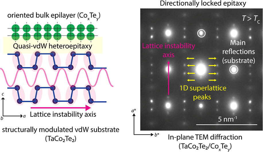
The material at the center of this approach is a layered compound called TaCo2Te2. Like graphite, its layers are held together by weak van der Waals forces, which makes it easy to combine with other materials without demanding a perfect chemical match. Unlike most layered crystals, though, its atoms are not arranged in a perfectly regular pattern. At room temperature they undergo a small, periodic shift known as a Peierls distortion, a phenomenon first described in the 1930s by the physicist Rudolf Peierls, who showed that in some materials the electrons and the surrounding lattice can lower their combined energy by nudging atoms slightly out of their ideal positions. When TaCo2Te2 is heated above about 523 kelvin, or 250 degrees Celsius, this distortion disappears and the crystal adopts a more symmetric structure, although traces of the original pattern linger as fleeting, temperature-driven fluctuations.
These fluctuations are not random. Calculations of how the crystal vibrates, backed up by Raman spectroscopy and electron diffraction experiments, show that the lattice is especially unstable along one crystallographic direction, meaning atoms can shift more easily there than in the perpendicular direction. This directional softness turns out to be the key ingredient that controls how a second material grows on the surface.
Heating TaCo2Te2 also sets its atoms in motion across the surface. Tantalum atoms drift away, while cobalt and tellurium reorganize into a thin crystalline layer whose composition resembles cobalt telluride. Rather than clumping into isolated islands, this new layer spreads sideways first and only then thickens, producing a smooth, continuous interface with the crystal beneath it, a layer-by-layer growth style that electron microscopy confirms is energetically favorable.
Directionally locked
The most striking result is that the new crystal does not settle into just any orientation. Even though its symmetry differs from that of the underlying TaCo2Te2, it becomes directionally locked. Along one in-plane direction, the atomic spacings of the two materials match closely, giving a tight, well-ordered registry. Along the perpendicular direction the mismatch is far larger, but this happens to be exactly the direction where TaCo2Te2 is most flexible, thanks to its lattice instability. Instead of rotating to relieve that mismatch, as symmetry-mismatched interfaces typically do, the interface absorbs it through a gentle, ongoing structural adjustment. The result is a crystal that stays aligned while only one direction bears most of the strain.
That flexible direction does not settle into a simple repeating pattern either. Instead, it forms what is called a one-dimensional incommensurate superlattice: the repeating atomic spacings of the two crystals never line up exactly, yet they stay locked together over long distances. Physicists have long recognized this kind of arrangement as an efficient way to accommodate mismatched lattice spacings without piling up large numbers of defects, since the strain is spread out through a slowly changing modulation rather than concentrated at sharp boundaries. Diffraction measurements and a geometric analysis of the two lattices both confirm that no perfectly repeating, shared lattice can account for what is observed, so the incommensurate description fits best.
Directional lattice instability is key
To check that the lattice instability is truly responsible for this behavior, the same experiment was repeated with a closely related compound, TaNi2Te2, which has nearly the same crystal structure but lacks the structural instability. Under similar heating, a surface layer still forms, but its orientation varies from spot to spot, and rotational disorder sets in. This comparison shows that matching crystal symmetry is not enough on its own to produce a locked, well-ordered interface. The directional lattice instability is the extra ingredient that guides the growth.
The local reconstruction effect
One more effect helps stabilize the interface. Even above the temperature where the bulk crystal should be fully symmetric, the atomic layers right beneath the interface partly slip back into the low-temperature distorted structure. This local reconstruction stays confined to the surface rather than spreading through the whole crystal, and it appears to strengthen the bond between the two materials, keeping the aligned structure stable even at high temperature.
As we have just seen, structural instabilities, usually considered as a liability because they signal that a crystal is on the verge of changing shape, can instead become useful design tools. A substrate whose atoms rearrange more easily in certain directions can guide the growth of otherwise incompatible materials, producing well-aligned interfaces without extensive surface treatment. This idea could widen the range of material combinations available for future electronic, optical, and quantum devices, where the atomic arrangement at an interface often determines how well the whole device performs.
Author: César Tomé López is a science writer and the editor of Mapping Ignorance
Disclaimer: Parts of this article may have been copied verbatim or almost verbatim from the referenced research paper/s.
References
Nitish Mathur, Guangming Cheng, Francesc Ballester, Gabrielle Carrel, Vincent M. Plisson, Fang Yuan, Jiangchang Zheng, Caiyun Chen, Scott B. Lee, Ratnadwip Singha, Sudipta Chatterjee, Kenji Watanabe, Takashi Taniguchi, Kenneth S. Burch, Berthold Jäck, Ion Errea, Maia G. Vergniory, Nan Yao, Sanfeng Wu, and Leslie M. Schoop (2026) Directionally Locked Heteroepitaxy with a Structurally Modulated van der Waals Material ACS Nano doi: 10.1021/acsnano.6c04146↩

 Login