
❌

Reading view

Cling film helps stamp two-dimensional materials onto patterned surfaces

Since the discovery of graphene over two decades ago now, two-dimensional (2D) materials have revolutionized almost all areas of science and technology thanks to their unique properties compared with bulk materials. These include high electronic conductivity, high mechanical strength, transparency and flexibility, to name just a few. The problem since the beginning, however, has been to produce sheets of these materials large enough for real-world applications and, importantly, to be able to transfer them onto other substrates without cracking the sheets. A team of researchers in Amsterdam, the Netherlands, has now succeeded in doing just this, with the help of an unexpected material – kitchen cling film. Their work could help in the continuing development of next-generation electronic and optoelectronic devices.

“The method we developed allows us to, for the first time, pick up, transfer and place large (roughly 1-mm-sized) 2D layers on almost arbitrarily patterned surfaces,” explains Jorik van de Groep of the 2D Nanophotonics group at the UvA-Institute of Physics, who led this research study. “Being able to do this is crucial since it enables the integration of 2D materials with structures like larger electronic devices and photonic coatings. Most importantly, the transfer is no longer probabilistic (as were most other methods) but has a near-unity yield.”

In the early days of 2D materials, researchers obtained micron-sized mono- or multi-layers of these structures by mechanically shaving off, or exfoliating, flakes from the bulk material using sticky tape. This was first famously done for graphene, a sheet of carbon just one atom thick. More recently, a technique known as gold-assisted exfoliation has allowed them to produce high-quality centimetre-sized layers of technologically important materials like transition-metal dichalcogenides (TMDCs) and transfer these onto flat glass surfaces.

For the field of nanophotonics in particular, explains van de Groep, we need to be able to transfer large-area 2D materials onto both flat and patterned substrates – such as those with electrical contacts and optical coatings on them, for example – if we are to fabricate functional devices. The problem is that existing transfer techniques are limited in this respect.

Kitchen cling film to the rescue

The Amsterdam team – which also includes researchers from UvA’s Van ‘t Hoff Institute for Molecular Sciences, ARCNL and AMOLF – has now developed a simple method that allows them to reliably transfer both large-area monolayers of TMDCs and hexagonal boron nitride/monolayer heterostructures onto patterned or non-patterned substrates, ranging from flat surfaces to high-aspect ratio and low adhesion patterned interfaces. In their process, which is detailed in ACS Nano, they used low-density polyethylene (LDPE), or kitchen cling film, an inexpensive and widely available polymer that has a low melting temperature.

In their work, the researchers transferred a gold-assisted-exfoliated large-area monolayer of the TMDC tungsten disulphide (WS2) from a silica (SiO2) substrate to another target SiO2 substrate. They began by fabricating a stamp made of a heat-resistant half-sphere covered by LDPE cling film. They then mounted the stamp on an xyz-micron precision stage and moved it slowly towards the WS2 monolayer, which was heated to 70 °C, at a speed of 0.5 µm/s until it contacted with the LPDE.

“We used force sensors in the stage to measure the forces involved during the stamping procedure, both in the plane of the 2D material (Fx and Fy) and perpendicular to it (Fz),” explains van de Groep. “This not only offers better control and repeatability of the transfer, it also provides crucial information on the contact and friction dynamics throughout the process.”

During initial contact with the substrate, the normal force (Fz) increases to 120 mN, at which point the researchers stop moving the stamp. Once it has contacted the monolayer, they heat the system to 140 °C. This induces a phase transition at which the LDPE melts, so allowing it to strongly adhere to the monolayer. They then cool the ensemble back down to 70 °C to solidify the LDPE. Finally, they pull off the monolayer from the LPDE with the stage moving at 0.5 µm/s and clean it to remove any polymer residue.

Material retains its good photoluminescence properties

To assess how the transfer process affects the monolayer, the researchers imaged it before and after the procedure. Before transfer, cracks covered 8% of the material. This figure increased to 14% after, with the cracks mainly generated at the edge of the stamp contact area. “As such, the procedure only modestly increases the cracked area fraction and largely preserves the monolayer topography,” says van de Groep. “More importantly, the material retains its good photoluminescence properties.”

The new work could help 2D materials scientists working in a variety of different fields to build larger and more complex devices. “Already, we are using it to develop atomically thin optical elements, optical modulators, single-photon emitters and other optoelectronic devices,” van de Groep tells Physics World. “Also, and more fundamentally, the method we have developed could allow for the fabrication of complex heterostructures of interest for quantum materials.”

The Amsterdam team is now busy optimizing its method further by, for example, building a humidity-controlled environmental enclosure around the stamping setup. “2D materials and the (van-der-Waals) adhesion between them strongly depends on the surface chemistry and, as such, on the relative humidity during the stamping procedure,” explains van de Groep. “We’re also working on additional methods to characterize the thickness of the materials in situ, that is, during the stamping process.”

The post Cling film helps stamp two-dimensional materials onto patterned surfaces appeared first on Physics World.
  •  

Two-dimensional material shows promise for long-term memory, thanks to slow electrons

Two-dimensional (2D) materials have attracted a lot of attention in recent years for their excellent electronic, thermal and mechanical properties, as well as their interesting quantum effects. While graphene has gathered the most commercial attention, there are hundreds of 2D materials, all of which have different combinations of properties for different applications. A research team headed up at the University of Chicago has discovered some unusual behaviour in the 2D material Fe5GeTe2.

Some 2D materials exhibit superconductivity properties and charge orders (in which the electrons are confined in a specific arrangement rather than being able to move freely). Charge orders arise from the reshaping of ground states in the electronic bands of a 2D materials to create flat electronic bands. And these flat bands cause the electrons to move very slowly in the lattice, at speeds much slower than expected.

Extremely flat electronic bands can often become incoherent, due to an ultrastrong electronic interaction strength between charge carriers. In research published in Science Advances, Shuolong Yang and colleagues found that Fe5GeTe2 exhibits a charge-ordered state where electrons move both collectively and very slowly, while remaining quantumly coherent.

“I was originally motivated by the fact that Fe5GeTe2 was discovered to host multiple structural phases with nearly the same stoichiometry. Each structural phase is associated with its unique electronic and magnetic phase,” says Yang. “These different structural phases have almost degenerate energies, which means that they can all be stabilized at room temperature.”

According to Yang, this discovery prompted two key research questions: What is the nature of each phase? Can we utilize these nearly energy-degenerate phases to encode information?

Fe5GeTe2 is part of specific class of 2D materials called van der Waals magnets, which could be used to develop new memory technology. The researchers probed the electronic structure and magnetic states of Fe5GeTe2 using angle-resolved photoemission spectroscopy (ARPES). “We were able to surgically probe the electronic band structure of each individual phase region (tens of microns in size) and figure out the physics,” Yang tells Physics World. “This immediately allows us to answer the question of ‘What is the nature of each phase?’”

After discovering that the electronic band was flat in Fe5GeTe2, further studies into the material showed that the charge order in Fe5GeTe2 was caused by the folding of electronic bands in the Brillouin zone within 30 meV of the Fermi level.

“We revealed a so-called Kondo-like phase, so the localized electronic states strongly interact with itinerant states, resulting in very peculiar, quantum coherent flat bands right at the Fermi level which dictates low-temperature transport,” says Yang. “The discovery of an effective Kondo lattice in a ferromagnetic phase [instead of magnetically non-ordered phase] is quite a surprise from a theoretical point of view, which forced us to go back to the drawing board to understand its physics. We think that that our surprising finding originates from a many-body localized state interacting with the conduction electrons.”

Because of the flat bands, the electronic system wants to spontaneously break the space-translation symmetry. It then forms a new superlattice order commensurate with the original lattice. “Our results provide the first experimental evidence that an interaction-driven flat band can itself drive electronic ordering through flat-band nesting, without relying on Moiré or geometrically frustrated flat-band engineering,” Yang explains. He notes that this “peculiar physics” used to be something obtained in delicately designed, twisted 2D materials. This finding, however, provides a new avenue to study complex many-body physics enabled by flat bands in stoichiometric and strongly correlated materials.

There’s the potential that the material’s different magnetic states could encode information for memory systems. This idea is being trialled by the team by using a micro-focused laser to switch between this observed quantum many-body phase and other phases.

“We’re using carefully designed laser pulses of different frequencies to switch between the multiple phases of Fe5GeTe2, including our discovered Kondo-like phase. If successful, we will utilize the many-body physics for some real memory operations,” Yang explains. This follow-on aims to tackle the second stated research question. However, to be practical, it will have to work at room temperature, and these quantum effects have so far only been realised at ultralow temperatures.

“Fundamental work is underway to understand the exact nature of this Kondo-like phase, whether it has any topological properties, and whether it connects to structural defects,” says Yang. “Eventually we want to understand how to microscopically describe such an exotic system.”

The post Two-dimensional material shows promise for long-term memory, thanks to slow electrons appeared first on Physics World.

  •  

Magnetic field first kills superconductor, then brings it back to life

Unconventional superconductors are poorly understood materials with exceptionally useful properties. One example is their response to magnetic fields. In conventional superconductors, applied magnetic fields suppress superconductivity by either breaking up the paired electrons that facilitate it (Cooper pairs) or introducing magnetic flux which introduce resistance when it moves through the material. However, in a few unconventional materials, competition between ferromagnetic ordering, where the magnetic moments align to point in the same direction, and superconducting ordering, where paired electron moments point in opposite directions, can lead to a phenomenon known as re-entrant superconductivity (RSC). This is where, in an applied field, the magnetic ordering will at first destroy superconductivity, but when the field increases further, the superconductivity reappears.

An international team of physicists led by Denis Maryenko of Japan’s RIKEN Center for Emergent Matter Science has now observed this phenomenon for the first time in a two-dimensional (2D) unconventional superconductor. “We did not look for the RSC, and it was extremely surprising that we saw that,” Maryenko tells Physics World.

2D or not 2D

RSC has previously been observed in three-dimensional ferromagnetic materials such as CeRh2As2, organic superconductors and possibly in so-called heavy fermion compounds such as UTe2. However, 2D materials have several advantages over 3D ones when it comes to superconductivity. For example, in the conductor MoS2, the material’s electronic band structure and spin-orbit coupling (SOC) combine to keep the electron spins pointing in a direction perpendicular to the sample’s surface. This locking greatly increases the value of the upper critical field, which is the maximum magnetic field at which superconductivity can persist.

Since 2D superconductivity had previously been observed at interfaces between KTaO3 and other materials, the RIKEN team took this as a starting point. “Our approach was to grow LaTiO3, [since] that has good lattice matching [to KTaO3], which is beneficial for epitaxial growth,” Maryenko explains.

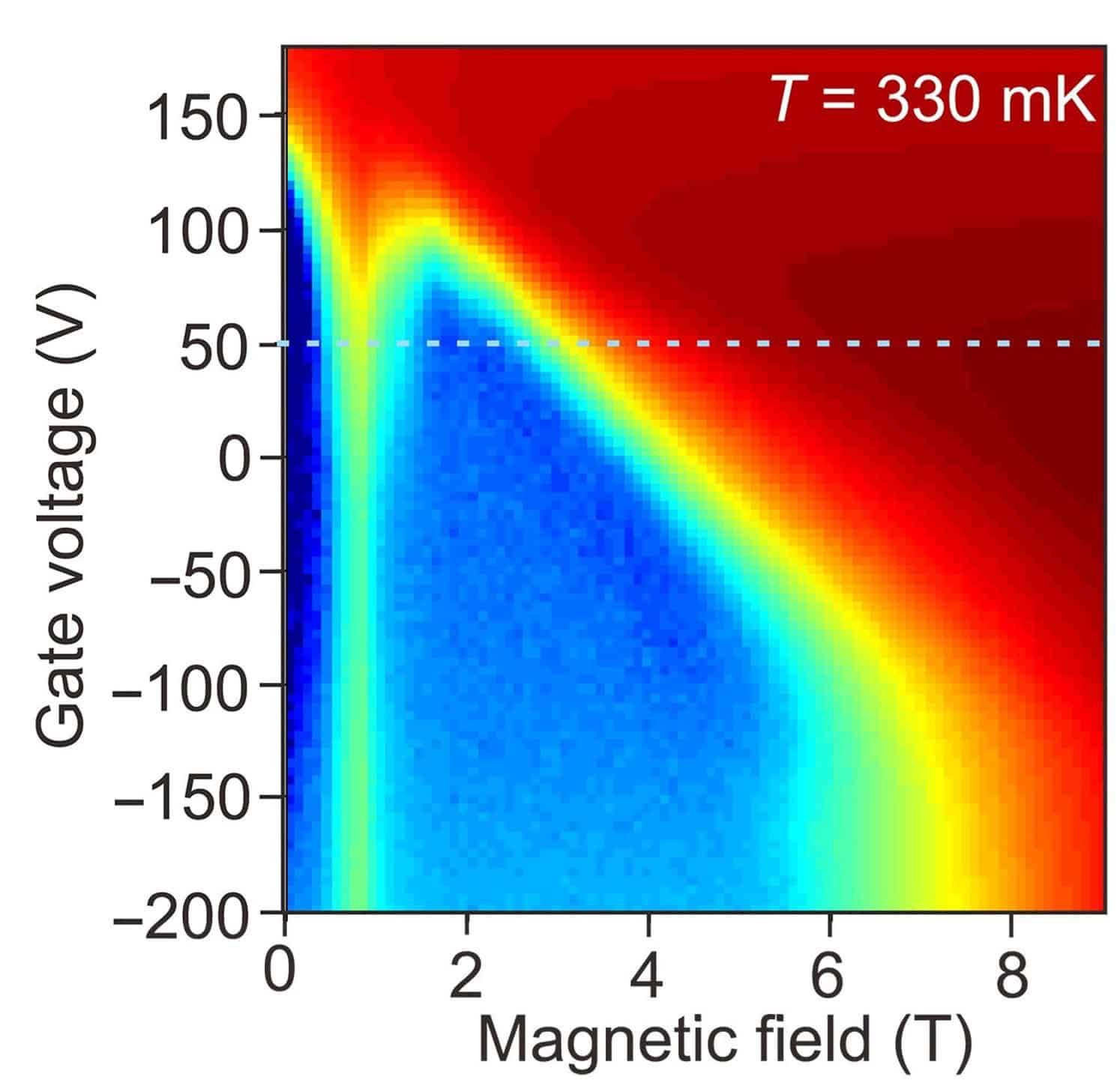
Writing in Science Advances, the physicists describe how they performed magnetotransport measurements on their LaTiO3/KTaO3 heterostructures to understand how these samples behaved in the presence of increasingly large applied magnetic fields. “We just wanted to see how the critical magnetic field behaves as a function of temperature, but suddenly we started seeing something else emerging at a rather low field: a resistive peak that seemed to separate two superconducting regions,” Maryenko says.

Rainbow colour plot of the interface resistance as a function of magnetic field and gate voltage. Higher gate voltages and magnetic fields are generally coloured red, but at a field of 0.9 T, there's a bright streak that appears to bleed down from the red area and stand out against the blue background.
Reentrant superconducting response: A plot of the interface resistance as a function of magnetic field and gate voltage, showing reentrant superconductivity at a magnetic field of around 0.9 T. (Courtesy: D Maryenko et al. Science Advances 12 26 DOI: 10.1126/sciadv.aeg0460)

This cusp, he explains, appears at a magnetic field B∗ of 0.9 T with zero resistance measured at both lower and higher applied fields. In this experiment, B∗ is independent of temperature and the concentration of charge carriers, which Maryenko and colleagues controlled experimentally by tuning a gate voltage across the interface.

Explaining re-entrant superconductivity

The researchers considered several possible explanations for the RSC, including Zeeman splitting, orbital effects and something called the Jaccarino-Peter effect, where internal and external magnetic fields compensate for each other and cancel out.

To identify the correct explanation, Igor Maznichenko and Sergey Ostanin from Martin Luther University in Germany and Arthur Ernst from Johannes Kepler University in Austria performed ab initio calculations to determine the electron band structure for the interface. These calculations identified the presence of a so-called Van Hove singularity, where for certain momenta, the electrons will have very high density of states.

Then, Vitalii Dugaev from Rzeszów University of Technology in Poland and Evgeny Ya Sherman at the University of the Basque Country in Spain developed a SOC-based model, taking inspiration from symmetry arguments and the ab initio band structure calculations. In the absence of an applied field, they found that there is a p ↔−p symmetry in the bands. This means that electrons with opposite momenta will have the same energy, so two electrons that form a Cooper pair, and have the same energy, have a total momentum equal to zero. In other words, the system favours spin-singlet Cooper pairs which form easily.

Applying a field breaks this symmetry, thereby reducing the Cooper pairing efficiency and decreasing the critical temperature Tc for the onset of superconductivity. On the other hand, the applied field also shifts the electrons closer towards the Van Hove singularity, increases the density of states and increases Tc. The combination of these opposing effects results in a minima appearing in Tc(B), hence RSC. The discovery of RSC in these materials establishes the system as a robust platform for studying unconventional superconductivity in 2D systems.

The post Magnetic field first kills superconductor, then brings it back to life appeared first on Physics World.

  •  

Encapsulation enhances surface structure imaging of 2D quantum material

Preserving MBT’s septuple-layer surface
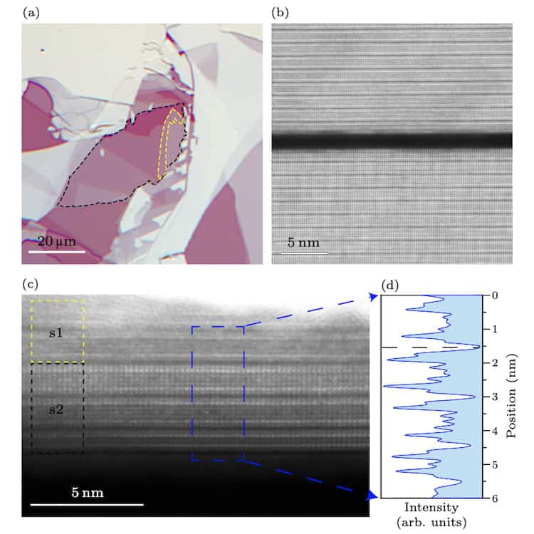
Surface preservation (a) Optical image of MBT-on-MBT sample, with the capping flake s1 and target flake s2 outlined in yellow and black, respectively. (b) TEM image of a homojunction interface with a thick capping layer, showing a substantial interface gap. (c) TEM image of an optimized interface using a thin capping flake s1 on the target s2. (d) The intensity profile extracted from the blue dashed box confirms that both the bottom surface of s1 and the top surface of s2 maintain a distinct seven-atom septuple-layer structure, demonstrating effective surface preservation. (Courtesy: Luo et al., Chin. Phys. Lett. 43 050713)

Thanks to a novel encapsulation technique, researchers at Fudan University in Shanghai, China, have succeeded in imaging the surface structure of the atomically thin topological quantum material MnBi2Te4 (MBT) for the first time. The work could help advance our understanding of the intrinsic properties of this technologically important class of materials and enable their use in novel devices.

The electronic, magnetic and topological properties of materials thinned down to atomic-scale thicknesses are very different to those of their bulk counterparts. They can, for example, be employed to study exotic quantum states that could prove useful for a host of advanced applications, such as next-generation spintronics and dissipationless electronics.

Before such devices see the light of day, however, we need to understand these emergent properties, which means accurately determining the surface atomic structure of these materials. This is no easy task because these surface structures are extremely sensitive to their environment. What is more, the most common technique used to study them, transmission electron microscopy (TEM), requires samples to be prepared as lamellae, which degrades them, changing their structure. The high-energy electron irradiation beam in the microscope does them no good either.

In the new work, a team led by Yuanbo Zhang of the State Key Laboratory of Surface Physics and department of physics at Fudan University, studied the topological quantum material MBT. This is the only intrinsic magnetic topological insulator made in the laboratory so far and can be used to study novel topological states – such as the quantum anomalous Hall effect and axion-insulator physics – many of which are fundamentally governed by surface states.

MBT’s surface is exceptionally vulnerable

Like other sensitive 2D materials, explains study co-author Jingjing Gao, MBT’s surface is exceptionally vulnerable to external perturbations, such as ambient air exposure, heat or standard electron microscopy preparation. These degrade the surface layer and irreversibly alter its structure. Indeed, a previous TEM study also revealed that the septuple-layer structure of an MBT flake transforms into a Bi2Te3-like quintuple layer configuration under ambient conditions.

To overcome this problem, Gao and colleagues developed a protective encapsulation technique that successfully shields the delicate surface structure of MBT from its environment and protects it during TEM sample preparation.

The researchers examined two types of encapsulating materials. The first was hexagonal boron nitride (hBN), which is chemically inert and already routinely employed to protect 2D materials. The second was a thin flake of MBT itself, which provides  a “homomaterial” capping layer. They encapsulated the MBT in one of these two materials immediately after they had exfoliated (or shaved off) flakes of MBT from a bulk sample. They did this inside an inert argon-filled glovebox.

An atomic-scale barrier

The protective layer acts like an atomic-scale barrier that isolates the MBT surface from oxygen, moisture, ion-beam damage and other environmental disturbances produced during the focused-ion beam processing used to prepare the samples for TEM. It also protects the MBT from the high-energy electron irradiation in the imaging microscope.

The researchers found that the homomaterial encapsulation is especially protective because the atomically similar layers can intimately contact with a minimal interfacial gap.

The technique strongly reduces defect formation, so the original lattice structure remains stable throughout the entire TEM workflow, explains Gao. “We therefore succeeded in safeguarding the ‘true’ surface throughout, allowing us to visualize the intrinsic septuple-layer structure at atomic resolution for the first time.”

The work will be important for both understanding intrinsic magnetic topological insulators and for developing quantum devices from these materials in the future, she tells Physics World. “Making such devices will demand exceptionally stringent requirements for sample surface and interface quality. This is because the MBT’s unique topological and magnetic properties are hosted by its surface states and even minor atomic reconstruction can distort its intrinsic quantum behaviour.”

Looking ahead, the researchers, who detail their work in Chinese Physics Letters, say they will now be looking to construct heterostructure devices with high-quality intrinsic surfaces and interfaces based on MBT. They will also make use of their encapsulation strategy to fabricate and study magnetic topological heterostructures.

“We will also explore topological superconductivity by interfacing MBT with superconductors, thereby advancing the development of topological quantum computing platforms,” reveals Gao.

The post Encapsulation enhances surface structure imaging of 2D quantum material appeared first on Physics World.

  •  

Altermagnets can turn neighbouring materials altermagnetic, too

Altermagnets can transfer their unusual magnetic properties to nonmagnetic materials placed next to them, say theorists in China and the US. This so-called “proximity effect” had already been observed in ferromagnets and superconductors, but it is new for altermagnets, which were only recognized as a distinct class of magnetic materials in 2024. If confirmed experimentally, the team says the effect could aid the development of advanced quantum materials with applications in fields such as spintronics, valleytronics and fault-tolerant quantum computing.

In ferromagnets, proximity effects make it possible to tune properties such as magnetic anisotropy, coercivity and exchange bias in nonmagnetic materials that have acquired magnetic polarization from a neighbouring ferromagnet. Similarly, ordinary materials that have picked up superconducting correlations from a nearby superconductor are a mainstay of experiments on topological superconductivity and topological quantum computing.

In the latest research, physicists led by Tong Zhou of the Eastern Institute of Technology in Ningbo sought to understand whether altermagnets could likewise transfer their behaviour to a neighbouring material. To do this, they created a model of a van der Waals bilayer heterostructure in which the bottom layer is a two-dimensional (2D) altermagnet, V2Se2O, while the top layer is a non-magnetic semiconductor, PbO.

Zhou explains that the vanadium atoms in V2Se2O form two opposite-spin sublattices that are connected by rotational symmetry rather than by simple translation or inversion. This complex structure is what gives V2Se2O its characteristic altermagnetic spin splitting, with a band structure in which spin-up and spin-down electrons have different energies that vary in periodic patterns. V2Se2O also has a so-called spin texture, which is a pattern of spin polarization that produces a net zero magnetization in the material.

First-principles calculations

Using first-principles calculations, the researchers found that the distinctive symmetry-patterned magnetism of V₂Se₂O can indeed transfer into the PbO layer across the interface between them. As a result, Zhou says the originally spin-degenerate bands of PbO develop a clear momentum-dependent spin splitting.

Importantly, this pattern is not arbitrary. Instead, it follows the symmetry expected from the altermagnetic order of V2Se2O. What is more, the real-space spin density of the PbO mirrors the symmetry of the V2Se2O, showing that it has inherited altermagnetism rather than simply becoming generically spin polarized.

When the researchers rearranged the V2Se2O into a conventional antiferromagnetic configuration with no alternating spin splitting, they found that the induced splitting in PbO disappeared. They also observed that the degree of induced splitting decreases when the PbO is placed further away from the V2Se2O, confirming the proximity effect.

As a final piece of evidence, the researchers searched for similar proximity effects in other altermagnetic systems, ranging from insulators to metals and covering material platforms with 3D architectures as well as 2D ones. “Even graphene, one of the most common 2D materials, can acquire altermagnetic characteristics when interfaced with CrSb, which is an experimentally well-established altermagnet,” Zhou notes.

Altermagnets as interfacial “spin-pattern generators”

One of the work’s main implications is that altermagnets could be used to generate spin patterns in many otherwise non-magnetic materials, Zhou tells Physics World. “This means that instead of searching only for intrinsic altermagnets, we can now design ‘proximitized’ altermagnetic systems by combining an altermagnet with a semiconductor, metal or superconductor,” he says.

In semiconductors, Zhou notes, the altermagnetic proximity effect can induce controllable spin and valley splitting, which are promising for spintronics and valleytronics devices, respectively. In superconductors, meanwhile, the effect can generate momentum-dependent spin splitting without the need to apply an external magnetic field or introduce net magnetization – something that Zhou says offers a new route toward topological superconductivity and the Majorana modes that could revolutionize fault-tolerant quantum computing. “More generally, this effect provides a versatile platform for designing field-free spin devices, topological quantum devices and multifunctional van der Waals heterostructures,” he says.

Looking ahead, Zhou and colleagues say they would now like to observe the altermagnetic proximity effect in heterostructures fabricated in the laboratory. They also want to find out how to control the strength of the effect – for example, by changing interlayer spacing, stacking, strain, gating and possibly even layer twisting.

“More fundamentally, an important question is how fast and how reversibly altermagnetic order, and therefore the altermagnetic proximity effect, can be reconfigured dynamically,” Zhou says. “That would be especially interesting for controlling spin-dependent transport and topological phases in real time.”

The research is described in  Physical Review Letters.

The post Altermagnets can turn neighbouring materials altermagnetic, too appeared first on Physics World.

  •  
❌