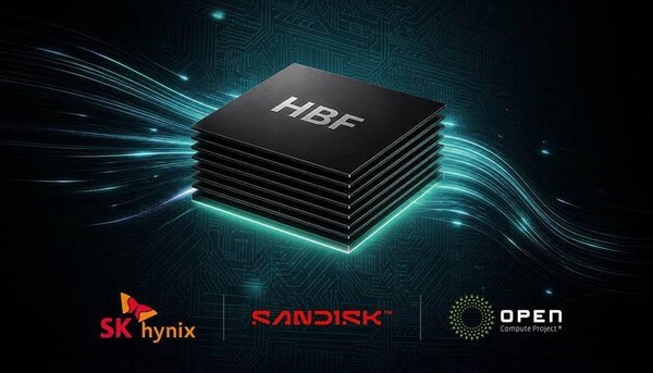
SanDisk will showcase next-generation NAND technologies, including HBF, at FMS 2026. (Photo: SK hynix)
SanDisk will showcase next-generation NAND technologies, including HBF, at FMS 2026. (Photo: SK hynix)
SanDisk announced on Aug. 6 that it will unveil next-generation NAND technologies for artificial intelligence (AI) applications at Future of Memory and Storage (FMS) 2026.
The technologies to be showcased include High Bandwidth Flash (HBF), next-generation NAND products and enterprise solid-state drives (SSDs). The solutions are designed for AI computing environments such as high-speed data lakes, model storage, retrieval-augmented generation (RAG) and key-value (KV) cache workloads. SanDisk plans to demonstrate how these technologies can address the diverse requirements of AI inference.
HBF is a NAND-based memory technology. Similar to High Bandwidth Memory (HBM), it vertically stacks NAND dies to increase data transfer speeds. The technology delivers high-bandwidth performance while offering greater capacity scalability than DRAM because it is NAND-based. HBF is designed for large-scale AI inference workloads that require both high bandwidth and large memory capacity.
SanDisk is participating in the HBF Specification Standardization Consortium alongside SK hynix. On Aug. 4, the consortium released its first HBF standard. The specification defines two configurations using eight-layer and 16-layer NAND die stacks. Maximum memory capacity is set at 512GB, while bandwidth is categorized into three performance tiers ranging from 0.4 terabytes per second (TB/s) to 3TB/s.
The company will also present its next-generation BiCS10 quad-level cell (QLC) NAND technology. The 3D NAND product is designed to improve density, performance and power efficiency to meet growing storage demand from AI data centers and cloud computing environments. SanDisk shipped samples of its BiCS10 triple-level cell (TLC) NAND last month.
In the enterprise SSD segment, SanDisk will showcase products based on the PCI Express (PCIe) 6.0 standard. The SSDs are designed in the E3.S form factor, a next-generation server storage specification. The products feature enhanced endurance for KV cache applications and reduced onboard DRAM requirements to maximize storage capacity. DRAM inside SSDs is typically used to store mapping tables that track the location of stored data.
The company will also introduce its AI Data Cycle Framework, an enhanced version of SanDisk’s proprietary framework designed to provide a comprehensive view of storage requirements across AI workloads. AI storage systems are used for functions including raw data archives, high-speed data lakes, model training, inference and generative content repositories.
“Growing inference workloads are creating demand for memory and storage technologies that can deliver optimal performance, capacity and power efficiency,” said Khurram Ismail, Chief Product Officer at SanDisk.
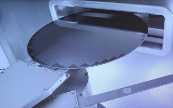
iVisionWorks is developing a semiconductor wafer inspection system. (Photo: KLA)
iVisionWorks is developing a semiconductor wafer inspection system. (Photo: KLA)
Machine vision inspection system company iVisionWorks has begun developing semiconductor wafer inspection equipment, the company announced on Aug. 5.
The new system will be a wafer metrology and inspection platform built on a high-sensitivity optical architecture. The market is currently dominated by overseas suppliers such as KLA and Hitachi High-Tech. iVisionWorks said it aims to develop a product that can compete on both defect detection capability and inspection speed.
The company plans to complete proof-of-concept (PoC) testing in the second half of this year and finish a prototype in the first half of next year. The prototype will then be used for customer evaluations.
Wafer inspection systems are used to identify defects generated during semiconductor manufacturing processes. Their performance has a significant impact on production yield and manufacturing efficiency.
Demand for wafer inspection equipment has been rising rapidly as the global expansion of artificial intelligence drives increased semiconductor production.
According to market research firm Fortune Business Insights, the global semiconductor defect inspection equipment market was valued at approximately $6.14 billion in 2025 and is projected to reach about $13.41 billion by 2034.
"We are concentrating our company-wide capabilities on entering the semiconductor inspection equipment market," said Gil Gi-jae, Chief Executive Officer of iVisionWorks.
"The semiconductor inspection equipment market has high technological barriers to entry, but we intend to leverage our accumulated precision optical technologies to establish a position in the sector and secure a new growth momentum," he added.
iVisionWorks currently supplies machine vision inspection equipment for secondary battery manufacturing processes.
Machine vision systems are automated measurement and identification platforms that combine optical hardware, software and image-processing technologies to inspect products and manufacturing processes.
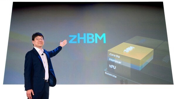
Kim Kyung-ryun, Vice President of DRAM Development at Samsung Electronics, introduces zHBM. (Source: Samsung Electronics)
Kim Kyung-ryun, Vice President of DRAM Development at Samsung Electronics, introduces zHBM. (Source: Samsung Electronics)
Samsung Electronics unveiled next-generation 3D memory technologies, including z-axis High Bandwidth Memory (zHBM) and zNAND-O, as the company seeks to strengthen its position in the rapidly growing artificial intelligence market.
Samsung on Aug. 5 showcased mockups of zHBM and zNAND-O for the first time at the Future of Memory and Storage (FMS) 2026 conference in California. During a keynote presentation on Aug. 4 local time, the company also outlined its vision for maximizing performance and power efficiency in high-performance computing (HPC) and AI systems through the use of zHBM, zNAND-O and other advanced memory technologies.
zHBM Delivers Up to Eight Times Higher Performance Through New Architecture
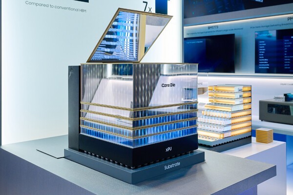
zHBM mockup. (Source: Samsung Electronics)
zHBM is a next-generation architecture that vertically stacks HBM on top of AI accelerators, or xPUs, along the z-axis. The design minimizes the distance data must travel between memory and AI processors, improving bandwidth and power efficiency while supporting the ultra-high-speed data processing required for training and inference of large-scale AI models.
Conventional architectures place HBM around the AI accelerator. Samsung said that approach faces limitations in meeting the performance requirements of next-generation HPC and AI infrastructure.
According to the company, zHBM can deliver up to eight times the data-processing performance of eighth-generation High Bandwidth Memory (HBM5) while improving performance per watt by a factor of three. Thermal resistance is reduced by more than half, enhancing both system stability and energy efficiency.
Samsung described zHBM as a customizable family of 3D memory products. The architecture allows customers to add semiconductor intellectual property (IP) blocks to an interlayer positioned between the memory and AI accelerator. These blocks can be tailored to expand memory capacity or optimize accelerator performance for specific workloads.
The company said it plans to work closely with customers to co-optimize AI processors and memory systems and maximize the performance potential of zHBM.
Samsung Reveals HBM-Like zNAND-O and 400-Plus-Layer V10 BV-NAND
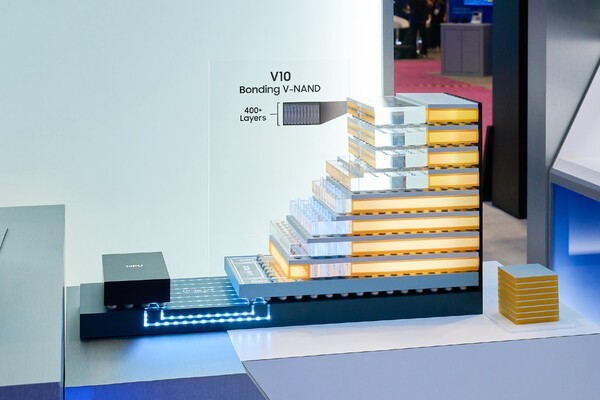
zNAND-O mockup. (Source: Samsung Electronics)
Samsung also introduced zNAND-O, a next-generation high-performance NAND flash family currently under development. The technology combines Samsung's vertical V-NAND stacking architecture with Through-Silicon Via (TSV) technology. TSVs are used in HBM to electrically and physically connect vertically stacked DRAM dies. Samsung's zNAND-O adopts a structure similar to High Bandwidth Flash (HBF), which is being developed by SK Hynix and Sandisk.
The "O" in zNAND-O refers to on-device AI applications. Samsung demonstrated four-layer and eight-layer 3D-packaged V-NAND configurations designed to deliver high space efficiency, increased read bandwidth and faster response times. The company said the technology is well suited for environments requiring real-time processing of large volumes of data.
During the keynote, Samsung also unveiled its V10 Bonding Vertical (BV)-NAND technology featuring more than 400 layers. The next-generation NAND architecture improves both performance and power efficiency. The displayed zNAND-O mockup was built using the V10 NAND platform.
BV-NAND separates the NAND cell array and peripheral circuitry onto different wafers before vertically bonding them together. The process utilizes advanced wafer-bonding technology that enables three-dimensional integration of multiple wafers.
Samsung further combines the approach with a three-stack architecture, in which V-NAND cells are manufactured in three separate stacks and then vertically interconnected. The company said memory density improves by approximately 58% compared with the previous V9 generation, enabling greater storage capacity within the same footprint. Read, write and input/output performance have also been enhanced.
HBM4E, HBM5 and Processing-in-Memory Technologies Also Displayed
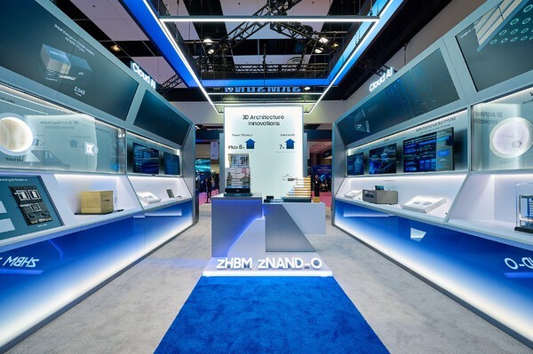
Samsung Electronics' exhibition booth at FMS 2026. (Source: Samsung Electronics)
Samsung's exhibition area featured more than 30 memory products spanning DRAM and NAND technologies. Highlights included a next-generation AI computing platform based on HBM4E, wafer samples, and an HBM5 mockup incorporating Heat Path Block (HPB) technology. HPB adds vertical heat-dissipation channels along the sides of HBM core dies to improve thermal management.
The company also showcased LPDDR5X-PIM, which combines low-power LPDDR5X DRAM with Processing-in-Memory (PIM) functionality. Samsung described the product as the world's first implementation of its kind, enabling more efficient data movement and improved power efficiency.
Storage products optimized for AI workloads were also displayed, including the PM1763 and BM1773. PM1763 is Samsung's next-generation enterprise solid-state drive (SSD), designed for high-speed reading and efficient data processing. BM1773 is an ultra-high-capacity enterprise SSD aimed at supporting large-scale AI training datasets.
Samsung emphasized that it remains the world's only integrated device manufacturer (IDM) capable of providing a one-stop solution spanning memory, logic semiconductors, foundry services and packaging.
"We can provide integrated services from the product design stage through mass production, helping customers shorten development cycles while optimizing performance and power efficiency," the company said. "This enables customized AI semiconductor solutions tailored to customer requirements."

 Login