❌

Reading view

Why an insulator can conduct electricity along its edges

Nickel disulfide, NiS₂, is an unusual material. Its interior behaves as an electrical insulator, blocking the flow of current, while certain parts of its surface conduct electricity freely. This contradiction has puzzled physicists for decades, and a recent study offers a detailed explanation. The conduction, it turns out, is confined to tiny one-dimensional steps on the surface, and these narrow conducting channels are a direct consequence of how electrons are arranged inside the crystal.

Mott insulator

NiS₂ shares its crystal structure with pyrite, the mineral sometimes called fool’s gold. At ordinary conditions, its electrons do not move freely through the lattice: the strong electrical repulsion between them opens an energy gap that keeps the bulk of the material insulating. This behaviour defines what physicists call a Mott, or charge-transfer, insulator, a category of materials that simple band theory cannot explain. Band theory predicts that any material with a partially filled outer electron shell should conduct electricity, yet compounds like nickel oxide obstinately insulate instead. In 1949, the physicist Nevill Mott showed why: if two electrons crowding the same atomic site cost more energy than is available, the electrons stay locked in place and no current flows, regardless of what band theory predicts. NiS₂ behaves in much the same way.

Yet electrical-transport measurements had repeatedly found that crystals of NiS₂ conduct through their surfaces. Earlier scanning-tunnelling experiments helped explain part of the puzzle: the broad, flat surface remains insulating, but the electronic gap narrows sharply near atomic-scale steps, tiny cliffs just one or two atoms high where the surface abruptly changes level. A new study 1 confirms this picture and examines the steps with much higher spatial resolution than before.

A not that smooth surface

A scanning tunnelling microscope (STM) works by bringing an extremely sharp needle close enough to a surface that electrons can leak across the gap between tip and sample. Measuring that leakage at different energies reveals both the surface’s shape and how easily electrons can enter or leave it. In NiS₂, these measurements uncovered electronic states concentrated tightly along the step edges: the states extend for a long distance parallel to a step but stay confined to roughly one to two nanometres across it. In other words, the electrons are effectively free to move in one direction while remaining trapped in the other two, forming genuine one-dimensional conduction channels.

NiS₂
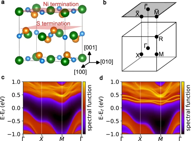
Surface spectra of the terminations observed in STM. Source: M. Iraola, H. Guo et al (2026) Nature Communications doi: 10.1038/s41467-026-76126-x

Two distinct kinds of surface step were observed, depending on whether the outermost atomic layer exposes nickel or sulfur atoms. Both carry electronic states associated with their steps, but they are not equally important. The nickel-terminated steps host states that sit right at the energy where electrical conduction happens, making them the most likely explanation for the surface conductivity that transport experiments had measured for years. The sulfur-terminated steps also host states inside the insulating gap, but their energy is positioned further away, making them less directly responsible for carrying current.

The study also tested what happens when a magnetic field is applied perpendicular to the surface. The step-edge states survived fields as strong as 10 tesla, a field far stronger than any produced by a laboratory magnet used for everyday purposes. Their intensity weakened somewhat, particularly on the sulfur-terminated steps, but the states were never destroyed. This robustness matters because NiS₂ already displays complicated magnetic behaviour of its own, which might easily have disrupted a more fragile conducting state.

The deeper explanation lies in how electrons are distributed inside the crystal. In an ordinary insulator, the occupied electronic states can usually be pictured as clouds centred on the atoms themselves. NiS₂ is different: calculations show that part of its electron density is naturally centred at special positions between atoms, specifically near the midpoints of pairs of sulfur atoms, where no atom actually sits. Physicists call these obstructed charge centres, and materials built around them belong to a class known as obstructed atomic insulators, a concept that grew out of a broader effort over the past decade to classify materials by the geometry, and not just the energy, of their electron states.

NiS₂
The concept of obstructed atomic insulator. In an OAI, the valence bands are induced from Wannier functions localized at obstructed Wannier charge centers (OWCCs)—symmetric positions in the crystal not occupied by any ion. Wannier functions are the localized molecular orbitals of crystalline systems. Source: M. Iraola, H. Guo et al (2026) Nature Communications doi: 10.1038/s41467-026-76126-x

Not ordinary metallic defects

This arrangement is not a chemical accident; it is protected by the symmetry of the crystal. When the crystal is cut to form a surface, though, the special positions that hosted this electron density can no longer fit together the way they did in the bulk. At a step edge, this mismatch creates what is known as a filling anomaly: an imbalance in how the available electronic states can be occupied, which leaves behind a state inside the insulating gap, localized right at the edge. Calculations of artificial step structures reproduce the main features seen under the microscope, including this localization, supporting the idea that the conducting channels are not ordinary metallic defects caused by broken chemical bonds, but a direct consequence of the crystal’s underlying electronic geometry.

The study also settles a long-standing question about NiS₂’s magnetism at low temperature. Below about 39 kelvin, the nickel magnetic moments arrange themselves into a non-collinear antiferromagnetic pattern, with neighbouring moments pointing in different directions that largely cancel out. Below about 30 kelvin, they rearrange again into a state that produces a small but measurable net magnetization. New neutron-diffraction measurements support a revised model of this low-temperature arrangement, resolving a debate about the material’s magnetic ground state that had lasted for roughly fifty years.

Taken together, the results give NiS₂ a significance well beyond its peculiar conducting surface. The material shows that strong repulsion between electrons, magnetism, and the geometry of electronic states can coexist within a single crystal. Such geometric protection is normally associated with topological materials, in which certain electronic states are shielded from disorder or defects by the crystal’s symmetry. The new results suggest that this protection can survive even when strong interactions push a material into being an insulator, making NiS₂ a rare setting for studying how the quantum-mechanical arrangement of electrons decides where electricity is allowed to flow within an otherwise insulating crystal.

Author: César Tomé López is a science writer and the editor of Mapping Ignorance

Disclaimer: Parts of this article may have been copied verbatim or almost verbatim from the referenced research paper/s.

References

  1. Mikel Iraola, Haojie Guo, Fabio Orlandi, Sebastian Klemenz, Martina O. Soldini, Sandra Sajan, Pascal Manuel, Jeroen van den Brink, Titus Neupert, Miguel M. Ugeda, Leslie M. Schoop & Maia G. Vergniory (2026) One-dimensional conduction channels in the correlated Mott NiS2 arising from obstructed Wannier charges Nature Communications doi: 10.1038/s41467-026-76126-x ↩

The post Why an insulator can conduct electricity along its edges appeared first on Mapping Ignorance.
  •  

A polymer membrane that grows its own arsenic-catching surface


Arsenic contamination in drinking water poses a critical global public health hazard. Prolonged exposure to inorganic arsenic—predominantly present in groundwater as arsenate, where arsenic exists in its +5 oxidation state—can lead to severe dermatological lesions, cardiovascular diseases, and cancers. To mitigate these health risks, the World Health Organization has established a strict provisional safety guideline of 10 micrograms of total arsenic per liter of drinking water. Because arsenic occurs naturally through the weathering of rocks and minerals in aquifers worldwide, engineering low-cost, scalable, and highly efficient materials for water purification remains a central goal in modern materials chemistry.

Iron-based compounds, particularly iron oxyhydroxides, are among the most effective materials for trapping arsenate. At a fundamental chemical level, arsenate ions readily substitute for surface hydroxyl groups on iron oxyhydroxides, forming strong chemical bonds that permanently anchor the contaminant to the solid surface. However, translating this surface chemistry into practical filters presents a persistent engineering hurdle: maximizing the amount of active iron exposed to water. Simply increasing the iron concentration during material synthesis causes iron nanoparticles to aggregate into large, dense clusters. As these clusters grow, much of the iron becomes buried within the interior bulk, leaving only a tiny fraction accessible at the surface to bind arsenate.

A promising design strategy 1 overcomes this limitation by decoupling the nucleation of iron particles from their subsequent growth on a flexible, high-surface-area polymer matrix. The foundation of this system is a composite fibrous membrane fabricated from poly(vinyl alcohol) and pectin via electrospinning. In electrospinning, a high-voltage electric field draws a liquid polymer mixture into ultra-fine threads, which solidify into an interconnected, highly porous mesh of nanofibers. Poly(vinyl alcohol) provides structural integrity and water stability upon heat treatment, while pectin—a natural polysaccharide rich in carboxyl and hydroxyl functional groups—serves as a molecular anchor capable of capturing iron ions from solution.

arsenic
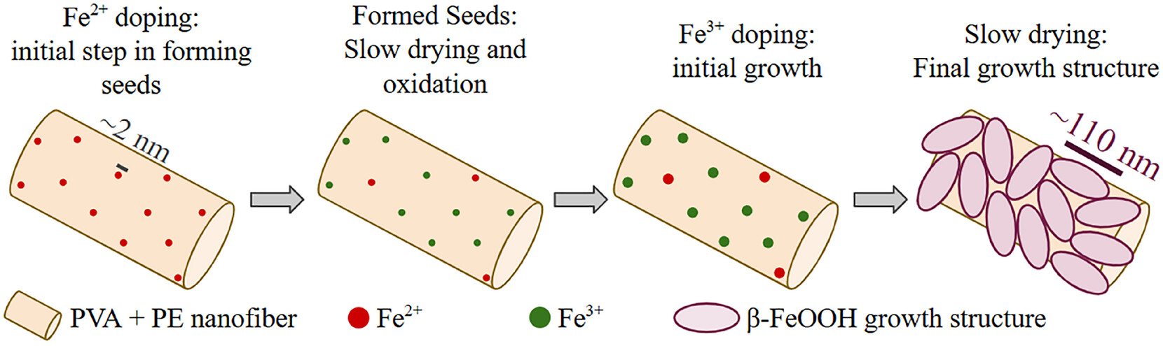
Proposed mechanism for anisotropic growth by an Fe seed. Source: A. C. Santos (2026) Small Methods doi: 10.1002/smtd.70975

To grow high-density nanostructures without triggering particle agglomeration, a sequential, two-step chemical treatment is applied. First, the electrospun membrane is immersed in a solution containing iron(II) ions (Fe2+). The carboxylate groups on the pectin molecules coordinate with these cations, forming uniformly dispersed, nanometer-scale iron seed clusters (~2 nanometers in size) across the nanofiber surfaces as the material dries and oxidizes. In the second step, the seeded membrane is placed in a solution containing iron(III) ions (Fe3+). Instead of forming isolated new particles in solution, the newly added iron deposits onto the pre-existing seeds, driving controlled anisotropic growth along preferred crystallographic axes.

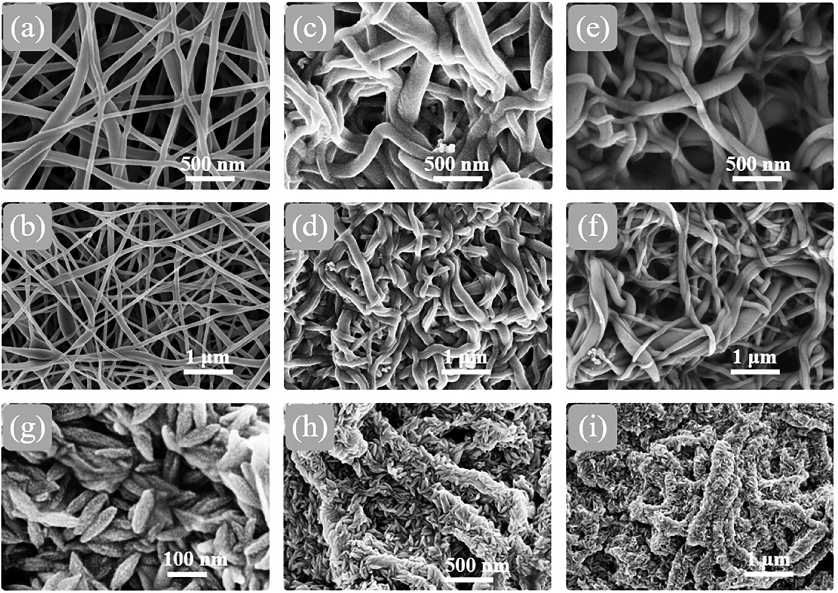
This seed-mediated approach yields an extraordinarily high density of surface-exposed iron nanostructures, achieving a 12-fold increase in surface atomic iron content compared to single-step doping methods. High-resolution electron microscopy reveals that these nanostructures adopt an elongated, rice-grain morphology measuring approximately 29 nanometers in width and 110 nanometers in length. Structural characterization using X-ray scattering, X-ray diffraction, and Mössbauer spectroscopy identifies the predominant active iron phase as akaganeite (β-FeOOH), a tunnel-structured, poorly crystalline iron oxyhydroxide known for its exceptional binding affinity toward arsenate.

arsenic
Field Emission Scanning Electron Microscopy (FE-SEM) micrographs for comparison of the morphologies of the composite mats with that of the reference PVA + PE membrane (a.b), which exhibits the typical electrospun nanofibrous structure. PVA + PE + Fe2 (c,d) and PVA + PE + Fe3 mats (e.f) retain a morphology similar to that of the pristine mats, whereas the PVA + PE + Fe2+Fe3 mat (g,h,i) is the only one exhibiting rice-grain-like structures along the nanofibers. The presence of these nanostructures indicates that the growth of the Fe-based structure was successfully achieved. Source: A. C. Santos (2026) Small Methods doi: 10.1002/smtd.70975

When evaluated in water purification tests, the nanostructured membrane demonstrates exceptional superadsorbent performance. Using a minimal material dosage of 1 gram per liter, the membrane reduces initial arsenate concentrations from 1000 micrograms per liter down to below 10 micrograms per liter within 24 hours at pH 6, achieving roughly 99% arsenic removal and satisfying WHO safety limits. The material retains high efficiency across a broad operational pH range of 5 to 8, and ICP analysis confirms that iron leaching into the treated water remains safely below 5 micrograms per liter.

Kinetic and isotherm analyses reveal that arsenate removal occurs via surface chemisorption governed by cooperative binding behavior. As initial arsenate molecules bind to active sites on the akaganeite surface, local chemical and electrostatic interactions make adjacent sites even more receptive to further adsorption, resulting in accelerated uptake kinetics. Furthermore, the material performs reliably in complex water environments. Naturally occurring co-contaminants such as fluoride do not interfere with arsenate capture, and the presence of heavy metal cations—such as copper and cadmium—actually enhances arsenate removal by forming secondary surface complexes that create additional binding sites. Although chemical regeneration using sodium hydroxide solution results in a slight decrease in capacity over repeated cycles due to incomplete desorption, the membrane maintains an 81% to 87% removal efficiency, demonstrating strong potential for practical, reusable water remediation systems.

Author: César Tomé López is a science writer and the editor of Mapping Ignorance

Disclaimer: Parts of this article may have been copied verbatim or almost verbatim from the referenced research paper/s.

References

  1. A. C. Santos, S. Cerveny, C. Iacovone, C. P. Ramos, A. J. Marzocca, and S. Goyanes (2026) High-Density Iron Nanostructures Grown on Electrospun PVA/Pectin Fibers via Seed-Mediated Strategy for As(V) Remediation Small Methods doi: 10.1002/smtd.70975 ↩

The post A polymer membrane that grows its own arsenic-catching surface appeared first on Mapping Ignorance.
  •  

Moiré collapse, when a twisted crystal becomes one-dimensional

One of the most striking discoveries in condensed matter physics over the past few years is that simply rotating one atomically thin crystal on top of an identical layer can create entirely new electronic behavior. This idea became famous in 2018, when physicists found that graphene sheets stacked at a very particular “magic angle” could turn into a superconductor, even though a single sheet of graphene is not. That discovery launched an entire field, sometimes called twistronics, built around moiré patterns: the large-scale interference patterns that appear when two crystal lattices are laid on top of each other with a slight mismatch in angle or spacing. In many materials, these patterns reshape how electrons move, sometimes producing superconductivity or other exotic collective states.

Moiré collapse

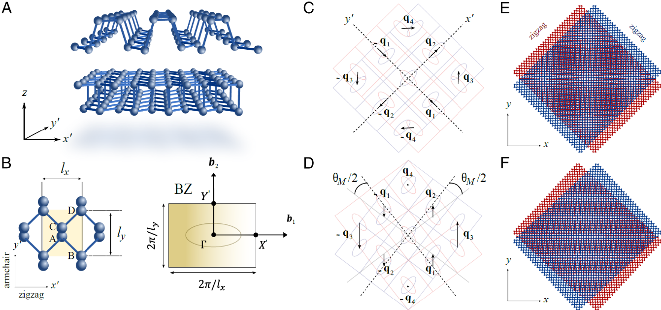
Most of this research has focused on materials whose crystal structure looks roughly the same in every direction, such as graphene, where the interesting physics shows up only at very small twist angles, close to perfect alignment. Now, a team of researchers instead looks at a strongly directional material: bilayer black phosphorus, whose atomic structure behaves very differently along two perpendicular directions in the plane, somewhat like a fabric that stretches easily one way but not the other. That built-in directionality turns out to change the whole logic of moiré physics, producing an effect the authors call moiré collapse. 1

Moiré collapse
Moiré collapse in twisted anisotropic homobilayers. Source: D. J. P. de Sousa et al. (2026) Proc. Natl. Acad. Sci. U. S. A. doi: 10.1073/pnas.2527371123 / fair use

In black phosphorus, the two layers start out rotated 90 degrees relative to each other. As that angle is dialed away from 90 degrees, the moiré pattern does something unusual. Rather than staying a two-dimensional pattern, like a slowly shifting checkerboard, it stretches more and more along one direction until, at a specific angle that depends only on the material’s own geometry, it effectively stops repeating in the other direction altogether. What remains behaves like a one-dimensional crystal, even though the material is still built from ordinary two-dimensional atomic sheets. For twisted bilayer black phosphorus, the calculations place this collapse at a twist of about 71.6 degrees, or equivalently about 18.4 degrees away from the initial 90-degree arrangement.

Pure geometry

This transformation has nothing to do with how electrons repel or attract each other; it is pure geometry. The mathematical description of the moiré pattern, expressed in terms of the directions in which its periodicity repeats, is squeezed from two independent directions down to one. In ordinary space, this means the pattern keeps a well-defined repeat distance along one axis while stretching out indefinitely along the other, with no repeating pattern left in that direction at all.

Such a dramatic structural change reshapes the electrons riding on top of it. At the untwisted 90-degree configuration, the anisotropy of one layer happens to cancel out the anisotropy of the other, so electrons move about equally well in every in-plane direction. As the twist angle approaches the collapse point, that cancellation breaks down. The electron energy bands become sharply directional, and electrons increasingly travel along one preferred line rather than spreading across the plane. Their energy spectrum starts to show the telltale fingerprints of one-dimensional systems, including sharp spikes in the density of available electron states known as one-dimensional van Hove singularities.

Luttinger liquid physics

One-dimensional conductors behave very differently from ordinary metals. In a three-dimensional metal, electrons can mostly be treated as independent particles that only weakly notice one another. Confine them to a single dimension, however, and that picture stops working: electrons cannot slip past each other, so they are forced to move collectively, in a coordinated wave-like fashion. The framework that describes this collective behavior, called Luttinger liquid theory, traces back to work by Sin-Itiro Tomonaga in 1950 and Joaquin Luttinger in 1963, and it has since been confirmed experimentally in systems such as carbon nanotubes. In a Luttinger liquid, the basic excitations are not single electrons at all, but collective ripples of charge and spin, and this leads to electrical transport properties that look qualitatively different from those of a normal metal.

The calculations in this study show that moiré collapse naturally sets up the conditions Luttinger liquid physics requires. As the collapse angle is approached, the one-dimensional electronic channels that form become progressively less coupled to their neighbors, making the correlated, wave-like behavior increasingly favorable. The analysis estimates a Luttinger parameter of about 0.3 for the collapsed black phosphorus system, a value indicating strong electron-electron interactions, and it predicts distinctive collective charge oscillations and unusual, non-metallic patterns in electrical conduction that could, in principle, be measured in the laboratory.

A notable feature of this mechanism is that the electron bands stay quite dispersive even at collapse, with electron speeds exceeding 100 kilometers per second. This sets it apart from most previously studied moiré systems, including twisted graphene, where strong correlations usually arise because the electronic bands become extremely flat and electrons effectively slow to a crawl. Here, the correlated behavior instead comes from the geometric collapse of the moiré lattice itself, with fast-moving electrons confined to one dimension rather than slow ones spread over two.

Moiré collapse is not a peculiarity of one material

To test these ideas, the researchers combined simplified mathematical models with detailed first-principles calculations of the atomic and electronic structure. Beyond black phosphorus, they found the same collapse in twisted bilayer tin selenide, another layered material with strongly directional bonding. The details of the electronic structure differ somewhat because of the specific atomic orbitals involved, but the same geometric collapse into quasi-one-dimensional channels appears, suggesting the phenomenon is not a peculiarity of one material but a general consequence of twisting any sufficiently anisotropic crystal.

Taken together, the findings outline a different strategy for engineering exotic quantum matter. Instead of hunting for a special magic angle that flattens electronic bands, as in twisted graphene, this approach relies on a purely geometric collapse angle at which a two-dimensional moiré material naturally turns one-dimensional. If confirmed in experiments, it would offer a new and versatile platform for studying Luttinger liquids and other correlated electronic phases that only emerge when electrons are squeezed into moving along a single line.


Author: César Tomé López is a science writer and the editor of Mapping Ignorance

Disclaimer: Parts of this article may have been copied verbatim or almost verbatim from the referenced research paper/s.

References

  1. D. J. P. de Sousa, S. Lee, F. Guinea, and T. Low (2026) Moiré collapse and Luttinger liquids in twisted anisotropic homobilayers Proc. Natl. Acad. Sci. U. S. A. doi: 10.1073/pnas.2527371123 ↩

The post Moiré collapse, when a twisted crystal becomes one-dimensional appeared first on Mapping Ignorance.
  •  

A new route to photon upconversion

Turning low-energy light into higher-energy light seems to break the usual rules of physics, since energy is supposed to run downhill, not uphill. Yet a process called photon upconversion achieves exactly this, without breaking any laws of thermodynamics. Instead of absorbing one photon and releasing a single photon of lower energy, as most light-absorbing molecules do, an upconversion system absorbs two lower-energy photons and combines their energy to release one higher-energy photon. Because it takes two photons to make one, the total energy is still conserved; the trick is repackaging it into a more useful form. The phenomenon was first observed in the 1960s in simple organic mixtures cooled to very low temperatures, but it only became practical decades later, once chemists identified metal-containing dyes able to hold their excited states at room temperature. Since then, scientists have pursued upconversion as a way to make better use of sunlight, to power light-driven chemical reactions, to improve imaging inside living tissue, and to build new kinds of optoelectronic devices.

Triplet-triplet annihilation

The most developed route to upconversion relies on a process called triplet-triplet annihilation. A light-absorbing molecule known as a sensitizer first captures a low-energy photon and passes that energy to a second type of molecule, the annihilator. The annihilator settles into a triplet excited state, an unusually long-lived condition that allows it to persist until it meets a second annihilator molecule in the same state. When two such molecules collide, one drops back to its ground state while the other is pushed up into a higher-energy singlet state, from which it emits a photon of higher energy than either of the photons that started the process.

A long-standing problem with this scheme is that ordinary sensitizer molecules lose a portion of the absorbed energy internally, as the initially excited state converts into the lower-energy triplet state that gets passed along. This loss caps how large an energy jump the whole system can ultimately achieve. One promising way around the problem is to replace the conventional sensitizer with an organic radical, a molecule carrying a single unpaired electron. That unpaired electron gives radicals unusual electronic and magnetic behavior and can make the conversion from absorbed light into a usable excited state considerably more efficient, since it opens transitions that are otherwise very weak in conventional molecules.

A single hydrogen to control it all

photon upconversion
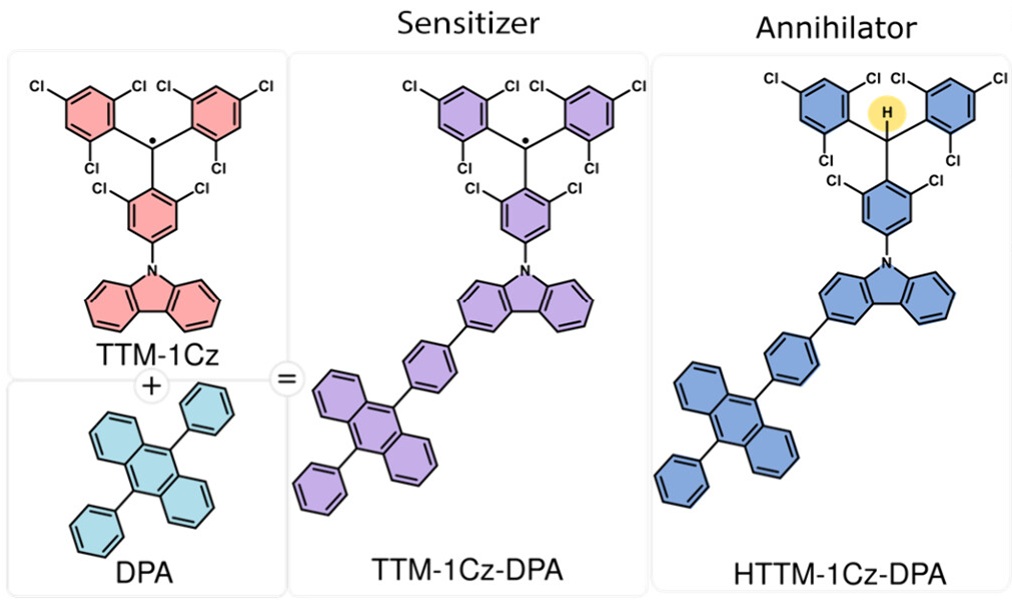
Chemical structures of open-shell TTM-1Cz [tris(2,4,6-trichlorophenyl)methyl – 1 carbazole] , DPA (9,10-diphenylanthracene), open-shell TTM-1Cz-DPA and closed-shell HTTM-1Cz-DPA.
New research examined 1 a pair of molecules built on this idea, both based on a radical component linked directly to an anthracene unit, the same type of light-emitting building block used in classic annihilators. The two molecules are nearly identical, differing at a single carbon atom: in one, that carbon carries the unpaired electron of the radical; in the other, an ordinary hydrogen atom has been added, pairing up the electron and removing the radical character entirely. That single hydrogen atom turns out to control everything. The radical version behaves as an efficient sensitizer, while the hydrogen-added version behaves as an annihilator, even though the two molecules share almost the same overall structure.

To work out why, the investigation combined light-based spectroscopy, electron spin resonance (a technique that detects unpaired electrons), and quantum chemical calculations. After the radical absorbs red light, its excitation transfers within about ten picoseconds (ten trillionths of a second) to the attached anthracene unit, creating a long-lived excited state that still carries some radical character. This internal handoff stretches the effective excited-state lifetime to more than 250 nanoseconds, roughly ten times longer than the 27 nanoseconds measured for the radical unit on its own. A longer-lived excited state gives the sensitizer far more opportunity to encounter another molecule and hand off its energy before simply decaying back to the ground state. The calculations independently pointed to the same conclusion, showing that energy transfer to a nearby annihilator proceeds far more readily through this long-lived triplet-like state than directly from the radical’s first excited state.

A mix needed

The work also tested an idea proposed in earlier research, that a single radical-containing molecule of this kind might act as both sensitizer and annihilator on its own, a so-called single-component upconversion system. The new experiments argue against this. Solutions containing only the radical molecule, across a range of concentrations, showed no detectable upconverted light, consistent with the radical’s higher excited states relaxing away too quickly for the necessary emission to compete.

Efficient upconversion instead required mixing the radical sensitizer with its hydrogen-added counterpart, or with the well-established annihilator 9,10-diphenylanthracene. Because the two molecules share nearly the same molecular framework, this two-molecule mixture is described as a “pseudo-single-component” system. Shining red light at 658 nanometres onto the radical paired with its hydrogenated twin produced blue emission at 450 nanometres, an apparent energy gain of about 0.9 electronvolts, with 7 percent of absorbed photon pairs converted into upconverted light. Pairing the same radical sensitizer with 9,10-diphenylanthracene instead produced blue emission at 437 nanometres, a slightly larger energy gain of about 1.0 electronvolt, with 12 percent efficiency. Both figures mark a large improvement over earlier all-organic radical sensitizers, which had reached efficiencies of only a few tenths of a percent, and the upconverted emission remained stable over hours of continuous illumination.

A practical strategy for photon upconversion

Beyond these specific molecules, the study illustrates how a minimal change in molecular structure, adding or removing a single hydrogen atom, can completely redirect a molecule’s photochemical role, switching it from an energy donor to an energy acceptor. Combining optical measurements, spin resonance, and computation made it possible to trace exactly why this switch occurs at the level of electronic structure, rather than simply observing that it happens.

The findings offer a clearer picture of how organic radicals can be harnessed for photon upconversion and point toward a practical strategy for building more efficient materials from radicals and their closed-shell relatives together. Such materials could eventually help capture more of the solar spectrum, drive light-powered chemical synthesis, or improve the efficiency of light-emitting technologies, by putting to use photons that would otherwise be wasted.

Author: César Tomé López is a science writer and the editor of Mapping Ignorance

Disclaimer: Parts of this article may have been copied verbatim or almost verbatim from the referenced research paper/s.

References

  1. Kieran D. Richards, Wenzhao Wang, Philipp Thielert, James D. Green, John M. Hudson, Claire Tonnelé, David Casanova, Yoann Olivier, Timothy J. H. Hele, Sabine Richert, Feng Li, and Emrys W. Evans (2026) Open- and Closed-Shell Roles of Sensitizer and Annihilator in Pseudo-Single Component Mixtures for Upconversion Journal of the American Chemical Society doi: 10.1021/jacs.6c04090 ↩

The post A new route to photon upconversion appeared first on Mapping Ignorance.
  •  

Rewriting the rules of heteroepitaxy with a flexible crystal

Building electronic devices often requires stacking different crystalline materials on top of one another with atomic precision. This process, called heteroepitaxy, works best when the two crystals share similar atomic patterns. When their symmetries differ, the upper crystal tends to grow in several orientations at once instead of a single one, creating defects that degrade device performance. Engineers have long dealt with this problem by treating the surface of the lower crystal beforehand, for example by etching steps into it, exposing it to plasma, or adding a buffer layer, to help the two materials bond more effectively. Now, a team of researchers explores 1 a different route: rather than forcing the two crystals to fit together, it takes advantage of a crystal that is naturally flexible at the atomic scale.

Flexible by design

flexible

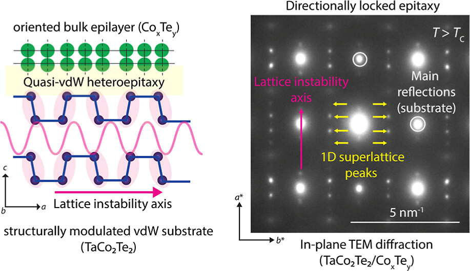
The material at the center of this approach is a layered compound called TaCo2Te2. Like graphite, its layers are held together by weak van der Waals forces, which makes it easy to combine with other materials without demanding a perfect chemical match. Unlike most layered crystals, though, its atoms are not arranged in a perfectly regular pattern. At room temperature they undergo a small, periodic shift known as a Peierls distortion, a phenomenon first described in the 1930s by the physicist Rudolf Peierls, who showed that in some materials the electrons and the surrounding lattice can lower their combined energy by nudging atoms slightly out of their ideal positions. When TaCo2Te2 is heated above about 523 kelvin, or 250 degrees Celsius, this distortion disappears and the crystal adopts a more symmetric structure, although traces of the original pattern linger as fleeting, temperature-driven fluctuations.

These fluctuations are not random. Calculations of how the crystal vibrates, backed up by Raman spectroscopy and electron diffraction experiments, show that the lattice is especially unstable along one crystallographic direction, meaning atoms can shift more easily there than in the perpendicular direction. This directional softness turns out to be the key ingredient that controls how a second material grows on the surface.

Heating TaCo2Te2 also sets its atoms in motion across the surface. Tantalum atoms drift away, while cobalt and tellurium reorganize into a thin crystalline layer whose composition resembles cobalt telluride. Rather than clumping into isolated islands, this new layer spreads sideways first and only then thickens, producing a smooth, continuous interface with the crystal beneath it, a layer-by-layer growth style that electron microscopy confirms is energetically favorable.

Directionally locked

The most striking result is that the new crystal does not settle into just any orientation. Even though its symmetry differs from that of the underlying TaCo2Te2, it becomes directionally locked. Along one in-plane direction, the atomic spacings of the two materials match closely, giving a tight, well-ordered registry. Along the perpendicular direction the mismatch is far larger, but this happens to be exactly the direction where TaCo2Te2 is most flexible, thanks to its lattice instability. Instead of rotating to relieve that mismatch, as symmetry-mismatched interfaces typically do, the interface absorbs it through a gentle, ongoing structural adjustment. The result is a crystal that stays aligned while only one direction bears most of the strain.

That flexible direction does not settle into a simple repeating pattern either. Instead, it forms what is called a one-dimensional incommensurate superlattice: the repeating atomic spacings of the two crystals never line up exactly, yet they stay locked together over long distances. Physicists have long recognized this kind of arrangement as an efficient way to accommodate mismatched lattice spacings without piling up large numbers of defects, since the strain is spread out through a slowly changing modulation rather than concentrated at sharp boundaries. Diffraction measurements and a geometric analysis of the two lattices both confirm that no perfectly repeating, shared lattice can account for what is observed, so the incommensurate description fits best.

Directional lattice instability is key

To check that the lattice instability is truly responsible for this behavior, the same experiment was repeated with a closely related compound, TaNi2Te2, which has nearly the same crystal structure but lacks the structural instability. Under similar heating, a surface layer still forms, but its orientation varies from spot to spot, and rotational disorder sets in. This comparison shows that matching crystal symmetry is not enough on its own to produce a locked, well-ordered interface. The directional lattice instability is the extra ingredient that guides the growth.

The local reconstruction effect

One more effect helps stabilize the interface. Even above the temperature where the bulk crystal should be fully symmetric, the atomic layers right beneath the interface partly slip back into the low-temperature distorted structure. This local reconstruction stays confined to the surface rather than spreading through the whole crystal, and it appears to strengthen the bond between the two materials, keeping the aligned structure stable even at high temperature.

As we have just seen, structural instabilities, usually considered as a liability because they signal that a crystal is on the verge of changing shape, can instead become useful design tools. A substrate whose atoms rearrange more easily in certain directions can guide the growth of otherwise incompatible materials, producing well-aligned interfaces without extensive surface treatment. This idea could widen the range of material combinations available for future electronic, optical, and quantum devices, where the atomic arrangement at an interface often determines how well the whole device performs.

Author: César Tomé López is a science writer and the editor of Mapping Ignorance

Disclaimer: Parts of this article may have been copied verbatim or almost verbatim from the referenced research paper/s.

References

  1. Nitish Mathur, Guangming Cheng, Francesc Ballester, Gabrielle Carrel, Vincent M. Plisson, Fang Yuan, Jiangchang Zheng, Caiyun Chen, Scott B. Lee, Ratnadwip Singha, Sudipta Chatterjee, Kenji Watanabe, Takashi Taniguchi, Kenneth S. Burch, Berthold Jäck, Ion Errea, Maia G. Vergniory, Nan Yao, Sanfeng Wu, and Leslie M. Schoop (2026) Directionally Locked Heteroepitaxy with a Structurally Modulated van der Waals Material ACS Nano doi: 10.1021/acsnano.6c04146 ↩

The post Rewriting the rules of heteroepitaxy with a flexible crystal appeared first on Mapping Ignorance.

  •  

Overcoming bottlenecks in bio-interface simulations: The MartiniSurf Approach

Enzymes and other biomolecules are often anchored onto solid materials so they can be reused, purified more easily, and made more stable, a strategy biotechnology has relied on since industrial-scale immobilized enzymes first appeared in chemical manufacturing in the mid-twentieth century. Immobilized enzymes today drive processes from food and pharmaceutical production to biosensors and medical diagnostics. Fixing a biomolecule in place, however, is not as simple as gluing it down. The exact spot where it attaches, the direction it faces, and how much freedom it retains to move can all change how well it works. Testing every possible arrangement in the laboratory is slow and costly, which is why computer simulation has become such a valuable complement to experiments.

The Martini force field

One of the main tools for this kind of study is molecular dynamics simulation, which calculates how atoms move over time by applying the basic laws of physics. Simulating every single atom of a protein, its surrounding water, and a supporting material gives rich detail, but is extremely demanding on computing power, especially when many attachment geometries need comparing. A widely used shortcut is coarse-grained modeling, in which small clusters of atoms are grouped into single, simplified particles. This keeps the essential physical behavior of the system while making the calculations far cheaper. The most established coarse-grained approach for biological molecules is the Martini force field, first developed in 2004 to describe fatty, membrane-forming molecules and later extended to proteins and, more recently, to a more accurate third generation of the model. Martini has since become a standard tool for simulating large biological assemblies that would otherwise be out of reach.

Introducing MartiniSurf

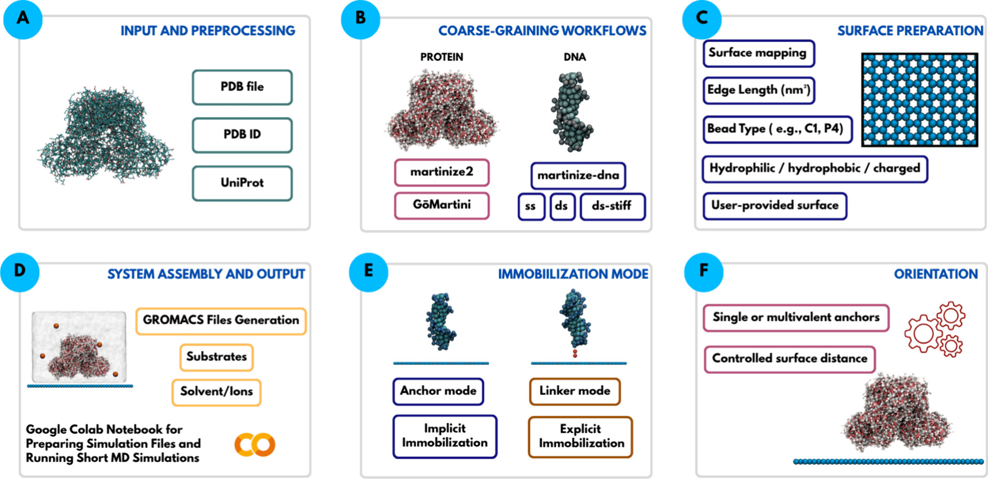
A team of researchers now introduces MartiniSurf 1, an open-source software package that automates the preparation of these coarse-grained simulations for biomolecules attached to surfaces. Building such a system by hand normally involves several separate programs and many manual steps, which makes it hard to reproduce results or compare different setups fairly. MartiniSurf instead combines the whole process into a single, streamlined workflow. Starting from the structure of a protein or a DNA strand, it converts the molecule into its coarse-grained form, builds a model of the supporting surface, positions the molecule in a chosen orientation, adds water and dissolved ions, and produces all the files needed to run the simulation with GROMACS, a molecular dynamics program that has been developed and refined for decades. Because every step is controlled by explicit settings rather than manual adjustments, two researchers using the same settings should obtain the same starting system, making comparisons across studies far more reliable.

MartiniSurf
Overview of the MartiniSurf workflow for constructing surface-immobilized biomolecular systems for coarse-grained molecular dynamics.

Restraining forces or linkers

A central feature of the software is its flexibility in representing how a biomolecule is attached. In one mode, selected regions of the molecule are held near the surface through simple restraining forces, without modeling the physical connector itself. In another mode, an explicit molecular linker is placed between the biomolecule and the surface, so that the linker’s own length and flexibility can influence the simulation. Because the properties of such linkers are known to affect how active and stable an attached enzyme remains, this second option offers a more realistic picture whenever the necessary coarse-grained description of the linker is available.

Variety of supporting surfaces

The supporting surfaces themselves can also be varied widely. The software can generate simple flat reference surfaces or draw on previously developed coarse-grained models of real materials such as graphene, graphite, carbon nanotubes, and agarose-like gels, the type of porous material commonly used to immobilize enzymes in the laboratory. Properties such as surface chemistry, electric charge, particle spacing, and added chemical groups can all be adjusted. Recent studies have shown that surfaces built without care can cause water molecules near the interface to line up in unrealistic, almost frozen patterns, an artifact rather than genuine physical behavior. The software includes options that let users introduce controlled irregularity into the surface to reduce this problem, while staying consistent with the wider Martini modeling framework.

In practice

To demonstrate how the approach works in practice, the study presents examples involving both proteins and DNA. For an enzyme attached to an agarose-like surface, the software reproduces several different attachment arrangements, including a complete system containing the enzyme together with its natural helper molecule and reaction substrate. These examples show how changing the attachment point or adding chemical groups to the surface can be explored systematically, without needing to reconstruct every model from scratch by hand.

The approach is also extended to DNA tethered to a graphene-like surface, comparing an electrically neutral surface with a positively charged one. The coarse-grained simulations reproduce the same general behavior previously reported in much more computationally demanding all-atom studies: the DNA strand remains mostly upright above the neutral surface but bends progressively toward the surface when it carries a positive charge, drawn in by electrostatic attraction. This comparison is not meant to reproduce exact experimental values, but rather to confirm that the automated setup captures the right physical trends, providing a check on the reliability of the workflow.

Reproducibility

Every simulation generated by the software automatically records the settings, software versions, and modeling choices used to build it, so that another researcher can repeat or directly compare a given calculation later. Importantly, the software does not introduce new physical models or new force-field parameters of its own. Instead, it draws on already validated Martini tools and organizes them into a consistent, automated pipeline.

Overall, MartiniSurf addresses a practical bottleneck in computational chemistry rather than proposing a new simulation method. By automating the construction of surface-bound protein and DNA systems, it makes coarse-grained molecular dynamics studies faster to set up, easier to reproduce, and simpler to scale across many attachment geometries. This kind of tool should make it easier to systematically study how surface properties, attachment geometry, and molecular flexibility shape the behavior of immobilized biomolecules, supporting the design of better catalysts, biosensors, and other biotechnology applications.

Author: César Tomé López is a science writer and the editor of Mapping Ignorance

Disclaimer: Parts of this article may have been copied verbatim or almost verbatim from the referenced research paper/s.

References

  1. J. C. Jimenez-Garcia, F. Lopez-Gallego, X. Lopez, and D. De Sancho (2026) MartiniSurf: Automated simulations of surface-immobilized biomolecular systems with Martini J. Chem Inf. Model. doi:10.1021/acs.jcim.6c00953 ↩

The post Overcoming bottlenecks in bio-interface simulations: The MartiniSurf Approach appeared first on Mapping Ignorance.
  •  

The Particle Odyssey: ITACA and the quest for neutrinoless double beta decay

One of the great unanswered questions in physics concerns the nature of neutrinos, the lightest known particles with mass. A process called neutrinoless double beta decay could provide the answer. In ordinary double beta decay, two neutrons inside a nucleus transform into two protons, emitting two electrons and two antineutrinos. In the neutrinoless version, only the electrons emerge. The idea has deep roots: in 1937 the Italian physicist Ettore Majorana proposed that some particles could be their own antiparticles, and two years later Wendell Furry realized that if neutrinos were such particles, double beta decay could occur without releasing any neutrinos at all. Observing this neutrinoless process today would confirm that neutrinos are indeed their own antiparticles and would show that a fundamental rule of particle physics, known as lepton number conservation, is not exact after all.

Chasing a decay that may never happen

The process, if it happens, must be extraordinarily rare. Current experiments are already sensitive to decays with half-lives greater than 10²⁶ years, far longer than the age of the Universe, and future detectors aim to probe even rarer events still.

One of the most promising technologies for this search uses xenon gas compressed to high pressure. When a charged particle moves through the gas, it ionizes xenon atoms and creates flashes of ultraviolet light. Electric fields then guide the liberated electrons toward sensors, allowing the event to be reconstructed in three dimensions. Xenon gas also allows exceptionally precise measurements of the energy deposited by the decay.

A neutrinoless double beta decay would release two electrons from a common point. As they travel through the gas, they follow winding paths and lose most of their energy at the ends of their trajectories, producing two small regions of concentrated energy deposition. This double-ended structure gives a characteristic signature that distinguishes the sought-after events from most background processes, which typically produce only a single electron track.

The main obstacle is that the drifting electrons spread out as they move through the gas. This diffusion blurs the image of the tracks, especially for events that occur far from the sensors. The amplification process used to make the faint electron signal detectable introduces further smearing. As a result, the distinctive two-electron pattern can become difficult to recognize, particularly deep inside large detectors.

ITACA (Ion Tracking with Ammonium Cations Apparatus)

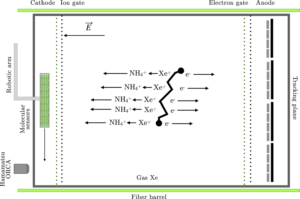
An alternative approach 1 is to image not only the electrons but also the positive ions left behind by the ionization process. Tiny amounts of ammonia (NH3), around one hundred parts per billion, can be added to the xenon gas. Rapid chemical reactions convert the positive xenon ions into ammonium ions (NH4+)almost as soon as they form, without significantly affecting the light signals or the transport of the electrons.

Itaca
Principle of operation of ITACA. Source: J. J. Gomez-Cadenas et al. (2026) Eur. Phys. J. C  doi: 10.1140/epjc/s10052-026-15501-w CC BY 4.0

These ammonium ions move far more slowly than electrons and diffuse much less along the way. Electrons cross the detector in a few milliseconds, whereas the ions can take anywhere from a fraction of a second to several seconds to reach their own collection point. Because the ion cloud stays comparatively compact, it can preserve fine details of the original interaction that may already be lost in the blurred electron image.

The two effects turn out to work against each other in a useful way. Wherever an electron happens to be born close to its collecting sensors, its own image stays sharp, while the corresponding ions still have most of their long journey ahead of them and their image comes out blurred. Deep in the gas, far from the electron sensors, the opposite happens: the electron image becomes badly smeared over its long drift, but the ions in that region have only a short remaining distance to travel and arrive with their picture largely intact. Because the two blurring effects are anti-correlated in this way, at least one of the two pictures, electron or ion, stays sharp no matter where in the detector a decay occurs, keeping the overall reconstruction quality close to uniform throughout the full detector volume.

itaca
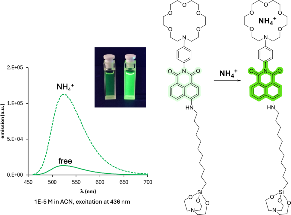
Emission spectra of the free and chelated species (with NH4+) of NAPH3 (Naphthalimide) sensors. Source: J. J. Gomez-Cadenas et al. (2026) Eur. Phys. J. C  doi: 10.1140/epjc/s10052-026-15501-w CC BY 4.0

The ion image itself is recorded by letting the ions land on specially prepared molecular surfaces coated with fluorescent sensors that respond specifically to ammonium ions. When illuminated by a laser, only the molecules that have actually captured an ion light up. A microscope and camera system can then scan this surface and reconstruct the ion track with very high spatial resolution.

The researchers call this system ITACA, after Ion Tracking with Ammonium Cations Apparatus. The researchers themselves would be Penelope, waiting for a husband and king who may, or may not, appear.

Would ITACA be the final destination?

Simulations indicate that these ion images preserve the characteristic two-endpoint structure expected from neutrinoless double beta decay, even in the presence of background noise from unbound sensor molecules that occasionally glow on their own. The sharper topology this provides should make it substantially easier to reject events produced by natural radioactivity and other processes that can otherwise mimic the sought-after signal.

Taken together, the additional information carried by the ion tracks could reduce troublesome background events by roughly an order of magnitude beyond what current xenon-gas detectors achieve, and by close to a factor of twenty for some of the most problematic radioactive backgrounds, those whose energy lies dangerously close to the signal itself. Improvements of this size would substantially increase the chances of finally catching neutrinoless double beta decay in the act, and with it, the chance to learn whether the neutrino holds one of the most unusual properties in all of particle physics.


Author: César Tomé López is a science writer and the editor of Mapping Ignorance

Disclaimer: Parts of this article may have been copied verbatim or almost verbatim from the referenced research paper/s.


References

  1. J. J. Gomez-Cadenas, L. Arazi, M. Elorza, Z. Freixa, F. Monrabal, A. Pazos, J. Renner, S. R. Soleti, and S. Torelli (2026) A journey to ITACA Eur. Phys. J. C  doi: 10.1140/epjc/s10052-026-15501-w ↩

The post The Particle Odyssey: ITACA and the quest for neutrinoless double beta decay appeared first on Mapping Ignorance.

  •  
❌