❌

Normal view

Unique zipper reaction converts perfluoroalkyl chains via defluorination and borylation

9 September 2026 at 17:22

In a development that could reshape how chemists recycle one of the most persistent classes of synthetic molecules ever made, researchers have reported a new catalytic strategy that strips fluorine atoms from perfluoroalkyl chains in a controlled, sequential fashion while installing a single boron group at the chain’s terminus. The work, published in Nature Communications, introduces what the authors call zipper polydefluorination-monoborylation, a transformation that walks down a perfluoroalkyl skeleton and removes multiple fluorine atoms in a stepwise cascade before capping the partially defluorinated product with a boron substituent. The achievement addresses a longstanding challenge in fluorine chemistry: while carbon-fluorine bonds are prized in materials and pharmaceuticals for their extraordinary stability, that same stability makes them notoriously difficult to break selectively, leaving chemists with few tools for converting perfluorinated waste streams into useful building blocks.

Perfluoroalkyl substances, often grouped under the umbrella of PFAS chemistry, owe their remarkable properties to the strength of the carbon-fluorine bond, which at roughly 485 kilojoules per mole in fully fluorinated chains ranks among the strongest single bonds that carbon forms. This bond strength, combined with the sheer electronegativity of fluorine, means that perfluoroalkyl groups resist oxidation, hydrolysis, and thermal degradation under nearly all conventional conditions. As a consequence, perfluorinated chains accumulate in the environment and resist standard degradation pathways, prompting intensive research into defluorination methods ranging from photocatalytic single-electron transfer to reductive hydrodefluorination with metal hydrides. Yet most existing approaches suffer from a common limitation: they either remove fluorine indiscriminately, collapsing the entire chain to a mixture of products, or they remove only a single fluorine atom, offering little control over the degree of defluorination. The new study demonstrates a way to achieve the best of both worlds, delivering multi-fluorine removal in a predictable pattern while simultaneously introducing a versatile functional handle.

The conceptual heart of the method lies in what the authors describe as a zipper mechanism. Rather than removing fluorine atoms at random positions along the chain, the reaction initiates at a defined site and then propagates along the perfluoroalkyl backbone one carbon at a time, much as a zipper opens tooth by tooth. At each step along the chain, a fluorine atom is expelled and replaced in sequence, with the reaction front advancing until a thermodynamic or kinetic stopping point is reached. The monoborylation component of the process ensures that once the zipper has run its course, the resulting olefinic or anionic intermediate is intercepted by a boron reagent, furnishing a product in which the boron group occupies a predictable position derived from the original perfluoroalkyl terminus. Organoboron compounds are among the most valuable intermediates in modern synthetic chemistry, serving as partners in Suzuki-Miyaura cross-coupling and as precursors to alcohols, amines, and halides, so their installation at a defluorination site effectively converts a chemical dead end into a synthetic launching pad.

Mechanistically, the transformation draws on the characteristic reactivity of organoboron reagents toward geminal difluoroalkenes, the partially defluorinated intermediates that arise when consecutive fluorine atoms are eliminated from a perfluoroalkyl chain. Perfluoroalkyl chains, when subjected to strong bases or reductive conditions, can undergo sequential beta-fluoride elimination events, each generating a more highly unsaturated species. The boron reagent in the reported system engages these unsaturated intermediates through addition pathways that install boron at the terminal carbon while generating a carbanionic center adjacent to the remaining difluoromethylene unit. That newly formed carbanion is perfectly positioned to expel another fluoride ion, regenerating an unsaturated handle one carbon further down the chain and setting up the next iteration of the cycle. This intimate coupling of borylation and defluorination is what gives the reaction its chain-walking character: each borylation event creates the conditions for the next defluorination event, and the process ripples along the chain until the fluorine reservoir is exhausted or the reagents are consumed.

The practical significance of the work becomes apparent when one considers the fate of the fluorine atoms themselves. In the zipper process, fluorine is released as fluoride ion, which under the reaction conditions is sequestered by silicon-containing trapping agents to form robust silicon-fluorine bonds. Fluorosilicates of this kind are stable, isolable, and, importantly, compatible with industrial processes for recycling fluorine back into hydrofluoric acid, the feedstock from which essentially all synthetic organofluorine compounds are made. In this sense, the method does more than transform perfluoroalkyl chains into borylated products; it also lays the groundwork for closing the fluorine cycle, recovering the fluorine content of persistent molecules in a form that can be fed back into the chemical economy. With global concern over PFAS contamination intensifying and regulatory pressure on fluorinated chemicals mounting, technologies that enable fluorine recovery rather than dilution into the environment carry considerable weight.

From a synthetic chemistry standpoint, the products of the reaction open multiple downstream avenues. Because the boron substituent is installed at a defined position on a partially fluorinated alkyl or alkenyl framework, the resulting molecules retain a programmable mixture of carbon-fluorine bonds and carbon-boron functionality. The remaining fluorine atoms can tune the lipophilicity, metabolic stability, and dipole moment of the scaffold, properties that are actively exploited in medicinal chemistry when designing fluorinated drug candidates. Meanwhile, the boron group serves as a convertible handle, allowing the defluorinated carbon center to be joined to aromatic rings through cross-coupling, oxidized to alcohols, or aminated in homologation reactions. In effect, the method converts a chemically inert perfluoroalkyl group, useful mainly as a passive coating or tail, into a functionalized partial-fluoro skeleton that can participate in the full toolkit of carbon-carbon and carbon-heteroatom bond formation.

The reported study also sheds light on the factors governing how far the zipper travels along a given chain. Chain length, the nature of the substituent anchoring the perfluoroalkyl group, and the stoichiometry of the base and boron reagent all influence the number of fluorine atoms removed and the distribution of products obtained. Through systematic variation of these parameters and careful analysis of the reaction mixtures by nuclear magnetic resonance spectroscopy and mass spectrometry, the authors map out the scope of the transformation across a range of perfluoroalkyl substrates, from short perfluoroethyl groups to longer chains approaching those found in commercial fluorosurfactants. Control experiments interrogating individual elementary steps support the proposed sequential elimination-addition mechanism and rule out alternative pathways involving radical fragmentation or random beta-scission, underscoring the unusually high degree of positional control the method achieves.

Beyond its immediate synthetic utility, the work contributes to a growing body of research aimed at taming the carbon-fluorine bond through the strategy of defluorinative functionalization. Over the past decade, chemists have developed an impressive repertoire of reactions that replace fluorine in perfluoroalkyl and fluoroarene substrates with groups ranging from hydrogen to sulfur, nitrogen, and carbon substituents. What distinguishes the zipper approach is its multiplicity and its directionality: instead of a single substitution event at a single site, the reaction performs many substitutions in a choreographed sequence along a chain, effectively treating the perfluoroalkyl group as a one-dimensional lattice to be patterned at will. This conceptual reframing, from defluorination as bond-breaking to defluorination as programmable editing, may inspire analogous strategies for other polyfluorinated motifs, including perfluoroarenes and perfluoropolyethers, two additional classes of highly persistent fluorinated materials.

Challenges remain before such chemistry can move from the laboratory bench to environmental remediation at scale. The reaction conditions reported rely on strong bases and moisture-sensitive boron reagents handled under inert atmosphere, and the substrates studied are discrete, soluble perfluoroalkyl compounds rather than the polymeric or adsorbed PFAS species that dominate environmental contamination. Scaling the chemistry will require sourcing boron reagents economically, managing the large quantities of fluoride generated, and integrating the transformation with upstream methods for extracting perfluoroalkyl pollutants from water and soil. Nevertheless, the demonstration that a perfluoroalkyl chain can be unzipped in a controlled manner, with fluorine captured in recyclable form and a valuable boron handle installed, establishes a credible chemical pathway toward defluorination that is both productive and selective, a combination that has eluded the field for decades.

As policymakers and scientists grapple with the legacy of fluorine chemistry, work of this kind illustrates a middle path between the wholesale abandonment of fluorinated molecules and their indefinite persistence in the biosphere. The fluorine atom confers properties that industry and medicine continue to depend upon, and the ability to disassemble fluorinated architectures on demand, recovering both the carbon skeleton as a functionalized building block and the fluorine content as a recyclable salt, points toward a more circular future for organofluorine chemistry. The zipper polydefluorination-monoborylation strategy reported in Nature Communications is an early but striking example of that vision made concrete at the molecular level, and it is likely to prompt rapid efforts to extend the concept across the breadth of persistent fluorinated chemicals.

Subject of Research: Controlled sequential defluorination of perfluoroalkyl chains coupled with terminal borylation (zipper polydefluorination-monoborylation)

Article Title: Zipper polydefluorination-monoborylation of perfluoroalkyl chains

Article References: Albers, S. L., Harzendorf, J. K., Deliaval, M., Köllmann, J., & Streuff, J. (2026). Zipper polydefluorination-monoborylation of perfluoroalkyl chains. Nature Communications, 17(1), Article 9502. https://doi.org/10.1038/s41467-026-77437-9

Image Credits: AI Generated

DOI: 10.1038/s41467-026-77437-9

Keywords: perfluoroalkyl chains, defluorination, polydefluorinative borylation, organoboron compounds, carbon-fluorine bond activation, PFAS degradation, fluorine recycling, geminal difluoroalkenes, cross-coupling, sustainable chemistry

More than 2,500 retired New York subway cars were dropped into the Atlantic between 2001 and 2010, not as illegal dumping but as a planned reef programme, and marine biologists who kept watch found the sunken trains quickly turned into some of the richest artificial habitats along the eastern seaboard.

9 September 2026 at 15:00

The Metropolitan Transportation Authority, which runs the New York City subway system, had a problem in the late 1990s. It was in the middle of a major fleet modernisation programme that was going to retire roughly two and a half thousand ageing subway cars over the following decade. These were mostly the red-painted R-33 and R-36 cars that generations of New Yorkers had ridden through the 1970s, 80s and 90s, followed by the older stainless steel Brightliners that would come off the tracks later. Each retired car was worth essentially nothing as scrap. Each also cost the MTA roughly twelve thousand dollars to dispose of through conventional demolition. Which meant the total disposal bill for the fleet retirement, at prevailing rates, was going to run to something north of thirty million dollars. And the MTA, being a public transit authority in a permanent state of budget crisis, was not enthusiastic about that particular expense.

The solution the agency arrived at, in partnership with a handful of coastal state governments and the U.S. Fish and Wildlife Service, was one of the more counterintuitive recycling programmes of the early twenty-first century. Instead of paying to demolish the cars, the MTA would clean them, ship them south by rail and barge, and drop them into the ocean off the eastern seaboard. There they would form artificial reefs. The states would get new marine habitat for essentially free. The MTA would save the disposal costs. And the fish would, in theory, work out what to do with the rest.

How you turn a subway car into a reef

According to the New York Transit Museum’s own summary of the MTA Artificial Reefing Program, produced in collaboration with the programme’s former director Michael Zacchea and Robert Martore of the South Carolina Department of Natural Resources, the operation ran from August 2001 through to April 2010 and deployed more than 2,500 deaccessioned train cars to underwater sites off the coasts of New Jersey, Delaware, Virginia, South Carolina, and Georgia. The first phase concentrated on the Redbird fleet, which was already being pulled off the tracks in 2001, and which had a particularly recognisable red livery that made the sunken cars a photographable subject long after they had gone down. The Delaware Bay took approximately six hundred and nineteen Redbird cars alone, at a site now known as the Redbird Reef, located sixteen and a half nautical miles off Indian River Inlet at a depth of around eighty feet. Subsequent phases involved the stainless steel Brightliner fleet, which was deployed at reef sites further down the coast through the second half of the decade.

The engineering of the actual reef deployment was not trivial. Each car had to be stripped down first. According to the New Jersey Division of Fish and Wildlife’s own news bulletin on the deployment of 44 stainless steel subway cars at the Atlantic City Reef site in April 2008, every car went through a full preparation process before it went into the water. Windows were removed. Wiring was pulled out. Plastic components, degradable materials, hydraulic fluids, oils, and grease were all stripped or drained. The remaining shell was inspected to make sure that when the car eventually corroded, nothing toxic would leach into the surrounding marine environment. Only after that inspection was the cleaned steel body loaded onto a barge and towed offshore.

The actual sinking process was almost comically straightforward. The cars, weighing around eighteen tonnes each in their prepared state, were rolled off the deck of the barge by a hydraulic tipping mechanism and simply dropped through the water column to the seabed below. The MTA covered all of the cleaning, transport, and deployment costs. Individual cars in the New Jersey deployment measured roughly sixty feet long, ten feet wide, and eleven feet tall. Deployed in tight clusters at pre-selected coordinates, they formed roughly the same kind of hard-structure habitat that a natural rocky reef would offer, but at a scale and geometry that had never previously existed on the sandy Atlantic continental shelf.

What the fish did with them

What happened next surprised the marine biologists monitoring the sites, though it probably shouldn’t have. The subway car reefs, unlike almost any natural feature of the mid-Atlantic seabed, offered vertical structure. They offered cavities and shelter. They offered hard surfaces for sessile organisms to colonise. And they were essentially unlimited in supply. Marine invertebrates began settling on the exposed steel within weeks. Barnacles arrived. Blue mussels followed. Sponges and soft corals began to establish themselves on the vertical surfaces. Within a year or two, the once-bare metal shells of the retired subway cars had become the physical scaffolding of thriving benthic communities that had not existed anywhere on that stretch of ocean floor beforehand.

The fish arrived in response. Delaware’s Department of Natural Resources and Environmental Control has since documented that the invertebrate communities colonising the artificial reef structures provide up to four hundred times more food per square foot than the bare sandy ocean floor they replaced. Species that had been effectively absent from the region because of the lack of suitable habitat began to appear regularly at the sites. Sea bass, tautog, tuna, mackerel, flounder, scup, and triggerfish were all documented in significant numbers within a few years of the deployments. Recreational fishing operators in the coastal towns of Delaware, New Jersey, and Virginia found their nearshore catches rising. Dive operators found themselves with a genuinely unusual attraction to offer. The sunken subway cars, which had cost the MTA nothing to dispose of and had cost the states essentially nothing to acquire, became one of the more productive artificial reef complexes anywhere on the North American Atlantic coast.

The programme was not without complications. Inspection reports from New Jersey in 2009 found that some of the newer stainless steel subway cars were showing significant structural damage after only a few years underwater, which prompted the state to pause further stainless steel deployments while investigations continued. Not every car remained intact. Not every deployment site delivered the ecological returns the biologists had hoped for. And the specific question of whether artificial reefs simply concentrate existing fish populations rather than creating new ones is still debated within the marine biology community. But the general pattern held across the majority of the deployment sites through the 2010s and 2020s. The bare sand became structured habitat. The structured habitat became invertebrate communities. The invertebrate communities became feeding grounds. And the feeding grounds became fisheries.

By the time the programme officially ended on Earth Day 2010, 2,580 New York subway cars had been placed on ocean reef sites along the eastern seaboard of the United States. The MTA had saved something close to thirty million dollars in disposal costs. Delaware alone had received nearly a thousand of them. The Redbird Reef off Slaughter Beach now covers roughly 1.3 square miles of what used to be featureless sand and is one of the most biologically productive stretches of continental shelf in the entire mid-Atlantic region. Which is a strange kind of legacy for a fleet of subway trains that once carried millions of people through the tunnels underneath Manhattan and Queens. The trains never made it to the recycling yard. They made it to the ocean floor instead. And the fish have been living in them ever since.

The post More than 2,500 retired New York subway cars were dropped into the Atlantic between 2001 and 2010, not as illegal dumping but as a planned reef programme, and marine biologists who kept watch found the sunken trains quickly turned into some of the richest artificial habitats along the eastern seaboard. appeared first on Space Daily.

Cling film helps stamp two-dimensional materials onto patterned surfaces

9 September 2026 at 09:00

Since the discovery of graphene over two decades ago now, two-dimensional (2D) materials have revolutionized almost all areas of science and technology thanks to their unique properties compared with bulk materials. These include high electronic conductivity, high mechanical strength, transparency and flexibility, to name just a few. The problem since the beginning, however, has been to produce sheets of these materials large enough for real-world applications and, importantly, to be able to transfer them onto other substrates without cracking the sheets. A team of researchers in Amsterdam, the Netherlands, has now succeeded in doing just this, with the help of an unexpected material – kitchen cling film. Their work could help in the continuing development of next-generation electronic and optoelectronic devices.

“The method we developed allows us to, for the first time, pick up, transfer and place large (roughly 1-mm-sized) 2D layers on almost arbitrarily patterned surfaces,” explains Jorik van de Groep of the 2D Nanophotonics group at the UvA-Institute of Physics, who led this research study. “Being able to do this is crucial since it enables the integration of 2D materials with structures like larger electronic devices and photonic coatings. Most importantly, the transfer is no longer probabilistic (as were most other methods) but has a near-unity yield.”

In the early days of 2D materials, researchers obtained micron-sized mono- or multi-layers of these structures by mechanically shaving off, or exfoliating, flakes from the bulk material using sticky tape. This was first famously done for graphene, a sheet of carbon just one atom thick. More recently, a technique known as gold-assisted exfoliation has allowed them to produce high-quality centimetre-sized layers of technologically important materials like transition-metal dichalcogenides (TMDCs) and transfer these onto flat glass surfaces.

For the field of nanophotonics in particular, explains van de Groep, we need to be able to transfer large-area 2D materials onto both flat and patterned substrates – such as those with electrical contacts and optical coatings on them, for example – if we are to fabricate functional devices. The problem is that existing transfer techniques are limited in this respect.

Kitchen cling film to the rescue

The Amsterdam team – which also includes researchers from UvA’s Van ‘t Hoff Institute for Molecular Sciences, ARCNL and AMOLF – has now developed a simple method that allows them to reliably transfer both large-area monolayers of TMDCs and hexagonal boron nitride/monolayer heterostructures onto patterned or non-patterned substrates, ranging from flat surfaces to high-aspect ratio and low adhesion patterned interfaces. In their process, which is detailed in ACS Nano, they used low-density polyethylene (LDPE), or kitchen cling film, an inexpensive and widely available polymer that has a low melting temperature.

In their work, the researchers transferred a gold-assisted-exfoliated large-area monolayer of the TMDC tungsten disulphide (WS2) from a silica (SiO2) substrate to another target SiO2 substrate. They began by fabricating a stamp made of a heat-resistant half-sphere covered by LDPE cling film. They then mounted the stamp on an xyz-micron precision stage and moved it slowly towards the WS2 monolayer, which was heated to 70 °C, at a speed of 0.5 µm/s until it contacted with the LPDE.

“We used force sensors in the stage to measure the forces involved during the stamping procedure, both in the plane of the 2D material (Fx and Fy) and perpendicular to it (Fz),” explains van de Groep. “This not only offers better control and repeatability of the transfer, it also provides crucial information on the contact and friction dynamics throughout the process.”

During initial contact with the substrate, the normal force (Fz) increases to 120 mN, at which point the researchers stop moving the stamp. Once it has contacted the monolayer, they heat the system to 140 °C. This induces a phase transition at which the LDPE melts, so allowing it to strongly adhere to the monolayer. They then cool the ensemble back down to 70 °C to solidify the LDPE. Finally, they pull off the monolayer from the LPDE with the stage moving at 0.5 µm/s and clean it to remove any polymer residue.

Material retains its good photoluminescence properties

To assess how the transfer process affects the monolayer, the researchers imaged it before and after the procedure. Before transfer, cracks covered 8% of the material. This figure increased to 14% after, with the cracks mainly generated at the edge of the stamp contact area. “As such, the procedure only modestly increases the cracked area fraction and largely preserves the monolayer topography,” says van de Groep. “More importantly, the material retains its good photoluminescence properties.”

The new work could help 2D materials scientists working in a variety of different fields to build larger and more complex devices. “Already, we are using it to develop atomically thin optical elements, optical modulators, single-photon emitters and other optoelectronic devices,” van de Groep tells Physics World. “Also, and more fundamentally, the method we have developed could allow for the fabrication of complex heterostructures of interest for quantum materials.”

The Amsterdam team is now busy optimizing its method further by, for example, building a humidity-controlled environmental enclosure around the stamping setup. “2D materials and the (van-der-Waals) adhesion between them strongly depends on the surface chemistry and, as such, on the relative humidity during the stamping procedure,” explains van de Groep. “We’re also working on additional methods to characterize the thickness of the materials in situ, that is, during the stamping process.”

The post Cling film helps stamp two-dimensional materials onto patterned surfaces appeared first on Physics World.

California’s Ambitious Plan for Textile Waste

8 September 2026 at 20:59
A recycling law coming into force now could change fashion.

© Jonathan Nackstrand/Agence France-Presse — Getty Images

A recycling center in Stockholm. California is trying to build a network for textile waste from scratch.

First switchable graphene nanoribbon that twists on demand

7 September 2026 at 14:00

Researchers at Nagoya University have built a graphene nanoribbon that can switch which way it twists using a natural solvent. Graphene nanoribbons are thin ribbon-shaped structures made of fused carbon rings. Twisted or helical versions of these ribbons show promise for advanced light and electronic devices. However, no graphene nanoribbon could switch that twist on demand, until now.

A 3D illustration of the [4]helicene nanoribbon shows the long chain of fused rings that gives the molecule its twisted structure. Source: Tomoyuki Ikai / Nagoya University
Scientists have worked out how to switch between a right-handed and left-handed twist (chirality) by changing the solvent around it. The discovery 1 opens opportunities for new optical switches, chemical sensors, and spintronic components that adapt to changing environments.

Tomoyuki Ikai, lead author and professor at Nagoya University’s Graduate School of Engineering, is a polymer chemist inspired by natural helical structures such as DNA and proteins. Polymers are large molecules built from many small, repeating units linked together in a chain. Ikai had been working on ladder polymers, where each repeating unit is locked into place and cannot freely rotate around the bond connecting to its neighbor (unlike a typical flexible linear polymer).

In 2019, Ikai and his collaborators built the first rigid, helix-shaped polymer. In 2021, they perfected a chemical method to fuse these building blocks together without flaws. This method is what let them build the new graphene nanoribbon.

“We used the same fusion approach already used to make predictable helical ladder polymers. But instead of a stable building block, such as [6]helicene, we used [4]helicene, a 4-ring unit written off as too unstable to be useful,” Ikai said.

Soak, twist, repeat

These units are difficult to control on their own because they switch their chirality too fast to hold one handedness. The team’s method fuses these small, restless units into one long chain. Once joined, they found that a neighbor effect took hold: each unit’s twist began to match its neighbors, and long stretches of the ribbon settled into a single, shared spiral.

To lock it in one overall direction, the researchers dissolved the ribbon in a natural chiral liquid, a liquid made of molecules that come in two mirror-image versions. They tested six candidates before they found the right one: beta-pinene, a compound found in pine trees and citrus peel.

Because beta-pinene molecules can be arranged in left- and right-hand mirror-images, these two versions each push the ribbon toward the opposite spiral. This also changed the twist direction of light the ribbon gave off, a property called circularly polarized luminescence, and is the first graphene nanoribbon shown to switch its light this way.

The switching induced a remarkably high degree of helical bias, with almost all of the helicene units aligning in the same direction. The switching effect is strongest at –90°C and grows weaker as the temperature rises toward room temperature.

“For a long time, people saw [4]helicene as unsuitable for chiral materials, because it could not be controlled,” Ikai said. “In this paper, we show that once you link enough of these units together, the instability itself becomes the useful part.”

A chiral solvent’s nudge toward one handedness is usually very weak on its own. Here, the ribbon’s own structure, with each unit mechanically linked to its neighbors, amplifies that weak nudge into a strong, nearly one-handed result.

An adaptive material

The researchers point to several possible future uses: The switchable light could serve optical devices. The ribbon’s chemical sensitivity to beta-pinene suggests it may work as a chiral sensor, and a similar design could one day help detect hazardous or unstable chemicals. Because graphene conducts electricity well, the ribbon may also suit electronic sensors.

The molecule’s twisted shape connects to spintronics, a field that uses the spin of electrons rather than just their charge. Ikai noted that a right-handed or left-handed structure can, in principle, let electrons of one spin pass through more easily than the other, a property helical structures are known for in physics literature.

The current design only holds its twist while it stays in the chiral liquid. If the solvent is removed, the ribbon drifts back to a mixed, unstable state. Ikai’s next goal is a form of “chiral memory,” a way for the ribbon to lock in its twist even after the solvent is gone. This next step builds on memory techniques the researchers have explored in other helical systems and is now applied to graphene for the first time.

References

  1. Ikai, T., Inagaki, H., Oki, K. et al. (2026) Dynamic helical poly[4]helicene nanoribbon. Nat Commun doi: 10.1038/s41467-026-76724-9 ↩

The post First switchable graphene nanoribbon that twists on demand appeared first on Mapping Ignorance.

China Installing Huge Facility That Turns Plastic Waste Into Jet Fuel

3 September 2026 at 19:41

Around the world, the demand for cleaner alternatives to petroleum-based jet fuel is rising.

By 2030, the European Union will require a minimum sustainable aviation fuel (SAF) blend of 6 percent, which will rise to 70 percent by 2050. Countries like the United Kingdom, Singapore, Japan, and Brazil are instituting similar policies, putting pressure on players in the global energy trade to ease reliance on crude oil.

SAF can come from all kinds of recycled waste byproducts like plant material, animal fat, and used cooking oil — the latter of which has already become a major source for existing SAF supplies. Unfortunately, the flow of extra spent fry oil is already slowing to a trickle as refiners swoop in to secure the gloop.

That’s where Chinese company Niutech comes in. In a new press release, first spotted by Interesting Engineering, Niutech announced a massive contract with an anonymous “global energy major” to build out an “industrial continuous waste plastic pyrolysis production line” capable of churning out 10,000 to 50,000 tons of plastic-derived SAF each year.

That might seem like a lot to unpack, but it’s really pretty simple. Basically, the Chinese firm is announcing the development of a massive supply line that turns plastic garbage into usable jet fuel. It plans to do so using a thermal decomposition process called pyrolysis, in which plastic waste is heated to extraordinary temperatures in an oxygen-free environment.

Though it isn’t new, pyrolysis remains something of a niche for the industrial-grade plastics-recycling space. For this approach to meet the growing need for SAF, it first has to graduate beyond the realm of small eco-startups into a widely-accepted industry standard — which appears to be Niutech’s goal.

Unlike previous SAF initiatives involving plastics, this particular production line will all be under one roof, cutting down on the need for costly shipping and handling. The Niutech refinery is also said to make use of a smorgasbord of plastics like polyethylene, nylon, polypropylene, and ABS, all “without complex pre-treatment such as washing, sorting or drying” — streamlining the complex process of sorting plastic and converting it to refinable oil at this kind of scale.

Should Niutech and its anonymous industry partner succeed in bringing the system online, it would undoubtedly serve as a constant source of plastics-based SAF for the global aviation industry, and as a role model for other refineries to follow.

“Large-scale pyrolysis projects impose stringent requirements on continuous operational capability,” a Niutech spokesperson said in the company’s press release. “Niutech has focused on pyrolysis technology for nearly 40 years and brings mature equipment and extensive project experience. This partnership is another validation of the strength of our industrial continuous technology.”

More on China: American Tech Companies Are Suddenly Sweating Bullets as China Catches Up on AI

The post China Installing Huge Facility That Turns Plastic Waste Into Jet Fuel appeared first on Futurism.

A polymer membrane that grows its own arsenic-catching surface

By: DIPC
3 September 2026 at 14:00


Arsenic contamination in drinking water poses a critical global public health hazard. Prolonged exposure to inorganic arsenic—predominantly present in groundwater as arsenate, where arsenic exists in its +5 oxidation state—can lead to severe dermatological lesions, cardiovascular diseases, and cancers. To mitigate these health risks, the World Health Organization has established a strict provisional safety guideline of 10 micrograms of total arsenic per liter of drinking water. Because arsenic occurs naturally through the weathering of rocks and minerals in aquifers worldwide, engineering low-cost, scalable, and highly efficient materials for water purification remains a central goal in modern materials chemistry.

Iron-based compounds, particularly iron oxyhydroxides, are among the most effective materials for trapping arsenate. At a fundamental chemical level, arsenate ions readily substitute for surface hydroxyl groups on iron oxyhydroxides, forming strong chemical bonds that permanently anchor the contaminant to the solid surface. However, translating this surface chemistry into practical filters presents a persistent engineering hurdle: maximizing the amount of active iron exposed to water. Simply increasing the iron concentration during material synthesis causes iron nanoparticles to aggregate into large, dense clusters. As these clusters grow, much of the iron becomes buried within the interior bulk, leaving only a tiny fraction accessible at the surface to bind arsenate.

A promising design strategy 1 overcomes this limitation by decoupling the nucleation of iron particles from their subsequent growth on a flexible, high-surface-area polymer matrix. The foundation of this system is a composite fibrous membrane fabricated from poly(vinyl alcohol) and pectin via electrospinning. In electrospinning, a high-voltage electric field draws a liquid polymer mixture into ultra-fine threads, which solidify into an interconnected, highly porous mesh of nanofibers. Poly(vinyl alcohol) provides structural integrity and water stability upon heat treatment, while pectin—a natural polysaccharide rich in carboxyl and hydroxyl functional groups—serves as a molecular anchor capable of capturing iron ions from solution.

arsenic
Proposed mechanism for anisotropic growth by an Fe seed. Source: A. C. Santos (2026) Small Methods doi: 10.1002/smtd.70975

To grow high-density nanostructures without triggering particle agglomeration, a sequential, two-step chemical treatment is applied. First, the electrospun membrane is immersed in a solution containing iron(II) ions (Fe2+). The carboxylate groups on the pectin molecules coordinate with these cations, forming uniformly dispersed, nanometer-scale iron seed clusters (~2 nanometers in size) across the nanofiber surfaces as the material dries and oxidizes. In the second step, the seeded membrane is placed in a solution containing iron(III) ions (Fe3+). Instead of forming isolated new particles in solution, the newly added iron deposits onto the pre-existing seeds, driving controlled anisotropic growth along preferred crystallographic axes.

This seed-mediated approach yields an extraordinarily high density of surface-exposed iron nanostructures, achieving a 12-fold increase in surface atomic iron content compared to single-step doping methods. High-resolution electron microscopy reveals that these nanostructures adopt an elongated, rice-grain morphology measuring approximately 29 nanometers in width and 110 nanometers in length. Structural characterization using X-ray scattering, X-ray diffraction, and Mössbauer spectroscopy identifies the predominant active iron phase as akaganeite (β-FeOOH), a tunnel-structured, poorly crystalline iron oxyhydroxide known for its exceptional binding affinity toward arsenate.

arsenic
Field Emission Scanning Electron Microscopy (FE-SEM) micrographs for comparison of the morphologies of the composite mats with that of the reference PVA + PE membrane (a.b), which exhibits the typical electrospun nanofibrous structure. PVA + PE + Fe2 (c,d) and PVA + PE + Fe3 mats (e.f) retain a morphology similar to that of the pristine mats, whereas the PVA + PE + Fe2+Fe3 mat (g,h,i) is the only one exhibiting rice-grain-like structures along the nanofibers. The presence of these nanostructures indicates that the growth of the Fe-based structure was successfully achieved. Source: A. C. Santos (2026) Small Methods doi: 10.1002/smtd.70975

When evaluated in water purification tests, the nanostructured membrane demonstrates exceptional superadsorbent performance. Using a minimal material dosage of 1 gram per liter, the membrane reduces initial arsenate concentrations from 1000 micrograms per liter down to below 10 micrograms per liter within 24 hours at pH 6, achieving roughly 99% arsenic removal and satisfying WHO safety limits. The material retains high efficiency across a broad operational pH range of 5 to 8, and ICP analysis confirms that iron leaching into the treated water remains safely below 5 micrograms per liter.

Kinetic and isotherm analyses reveal that arsenate removal occurs via surface chemisorption governed by cooperative binding behavior. As initial arsenate molecules bind to active sites on the akaganeite surface, local chemical and electrostatic interactions make adjacent sites even more receptive to further adsorption, resulting in accelerated uptake kinetics. Furthermore, the material performs reliably in complex water environments. Naturally occurring co-contaminants such as fluoride do not interfere with arsenate capture, and the presence of heavy metal cations—such as copper and cadmium—actually enhances arsenate removal by forming secondary surface complexes that create additional binding sites. Although chemical regeneration using sodium hydroxide solution results in a slight decrease in capacity over repeated cycles due to incomplete desorption, the membrane maintains an 81% to 87% removal efficiency, demonstrating strong potential for practical, reusable water remediation systems.

Author: César Tomé López is a science writer and the editor of Mapping Ignorance

Disclaimer: Parts of this article may have been copied verbatim or almost verbatim from the referenced research paper/s.

References

  1. A. C. Santos, S. Cerveny, C. Iacovone, C. P. Ramos, A. J. Marzocca, and S. Goyanes (2026) High-Density Iron Nanostructures Grown on Electrospun PVA/Pectin Fibers via Seed-Mediated Strategy for As(V) Remediation Small Methods doi: 10.1002/smtd.70975 ↩

The post A polymer membrane that grows its own arsenic-catching surface appeared first on Mapping Ignorance.

Two-dimensional material shows promise for long-term memory, thanks to slow electrons

2 September 2026 at 15:30

Two-dimensional (2D) materials have attracted a lot of attention in recent years for their excellent electronic, thermal and mechanical properties, as well as their interesting quantum effects. While graphene has gathered the most commercial attention, there are hundreds of 2D materials, all of which have different combinations of properties for different applications. A research team headed up at the University of Chicago has discovered some unusual behaviour in the 2D material Fe5GeTe2.

Some 2D materials exhibit superconductivity properties and charge orders (in which the electrons are confined in a specific arrangement rather than being able to move freely). Charge orders arise from the reshaping of ground states in the electronic bands of a 2D materials to create flat electronic bands. And these flat bands cause the electrons to move very slowly in the lattice, at speeds much slower than expected.

Extremely flat electronic bands can often become incoherent, due to an ultrastrong electronic interaction strength between charge carriers. In research published in Science Advances, Shuolong Yang and colleagues found that Fe5GeTe2 exhibits a charge-ordered state where electrons move both collectively and very slowly, while remaining quantumly coherent.

“I was originally motivated by the fact that Fe5GeTe2 was discovered to host multiple structural phases with nearly the same stoichiometry. Each structural phase is associated with its unique electronic and magnetic phase,” says Yang. “These different structural phases have almost degenerate energies, which means that they can all be stabilized at room temperature.”

According to Yang, this discovery prompted two key research questions: What is the nature of each phase? Can we utilize these nearly energy-degenerate phases to encode information?

Fe5GeTe2 is part of specific class of 2D materials called van der Waals magnets, which could be used to develop new memory technology. The researchers probed the electronic structure and magnetic states of Fe5GeTe2 using angle-resolved photoemission spectroscopy (ARPES). “We were able to surgically probe the electronic band structure of each individual phase region (tens of microns in size) and figure out the physics,” Yang tells Physics World. “This immediately allows us to answer the question of ‘What is the nature of each phase?’”

After discovering that the electronic band was flat in Fe5GeTe2, further studies into the material showed that the charge order in Fe5GeTe2 was caused by the folding of electronic bands in the Brillouin zone within 30 meV of the Fermi level.

“We revealed a so-called Kondo-like phase, so the localized electronic states strongly interact with itinerant states, resulting in very peculiar, quantum coherent flat bands right at the Fermi level which dictates low-temperature transport,” says Yang. “The discovery of an effective Kondo lattice in a ferromagnetic phase [instead of magnetically non-ordered phase] is quite a surprise from a theoretical point of view, which forced us to go back to the drawing board to understand its physics. We think that that our surprising finding originates from a many-body localized state interacting with the conduction electrons.”

Because of the flat bands, the electronic system wants to spontaneously break the space-translation symmetry. It then forms a new superlattice order commensurate with the original lattice. “Our results provide the first experimental evidence that an interaction-driven flat band can itself drive electronic ordering through flat-band nesting, without relying on Moiré or geometrically frustrated flat-band engineering,” Yang explains. He notes that this “peculiar physics” used to be something obtained in delicately designed, twisted 2D materials. This finding, however, provides a new avenue to study complex many-body physics enabled by flat bands in stoichiometric and strongly correlated materials.

There’s the potential that the material’s different magnetic states could encode information for memory systems. This idea is being trialled by the team by using a micro-focused laser to switch between this observed quantum many-body phase and other phases.

“We’re using carefully designed laser pulses of different frequencies to switch between the multiple phases of Fe5GeTe2, including our discovered Kondo-like phase. If successful, we will utilize the many-body physics for some real memory operations,” Yang explains. This follow-on aims to tackle the second stated research question. However, to be practical, it will have to work at room temperature, and these quantum effects have so far only been realised at ultralow temperatures.

“Fundamental work is underway to understand the exact nature of this Kondo-like phase, whether it has any topological properties, and whether it connects to structural defects,” says Yang. “Eventually we want to understand how to microscopically describe such an exotic system.”

The post Two-dimensional material shows promise for long-term memory, thanks to slow electrons appeared first on Physics World.

Delivering sound to a specific listener

1 September 2026 at 14:00

The kind of technology that can deliver sound to a single listener—like something out of a spy film—may soon become a reality. Researchers at Pohang University of Science and Technology (POSTECH) have developed a speaker system that can direct speech to a specific person. 1

Schematic of the ultrasonic transducer developed by the research team, integrating two types of metamaterials, together with the directional characteristics of transmitted voice signals. Source: POSTECH

Light and sound behave differently. Light from a flashlight or laser travels in a straight line, whereas sound readily spreads in all directions—that is why voices can be heard over a wall. The question, “Could sound, like light, be sent only where we want it?” led to the team’s highly directional speaker, MiPAL. By modulating ultrasound with audible content, the system can deliver sound only within a targeted area. A representative technology is the parametric array loudspeaker (PAL), which uses the nonlinear interaction of two ultrasonic waves in air to generate and concentrate audible sound in a specific direction.


Compared with conventional speakers, PALs can confine sound to a much narrower region. Traditional systems, however, require tens to hundreds of ultrasonic emitters to be precisely arranged and individually controlled, making them expensive and structurally complex. More recent PAL designs have simplified the hardware, but the vibrating diaphragm can also excite unwanted vibration modes, allowing sound to leak sideways and undermining directivity.


The team addressed this problem by integrating two types of metamaterials into a single ultrasonic transducer. An acoustic metasurface was mounted at the front. Acting like a lens for sound, it reshapes the irregular ultrasonic wavefronts radiated by the diaphragm into a straight, narrow beam, much like a laser. Elastic meta-units were placed at the rear. Acting more like a sound barrier, they suppress unwanted vibrations at selected frequencies and keep sound from leaking to the sides. In effect, the design uses a double safeguard: it focuses the sound at the front and blocks parasitic noise at the back.

Source: Kim, W. et al. (2026) Nat Commun doi: 10.1038/s41467-026-73604-0

As a result, the single-element device directed sound over a frequency range of 500 Hz to 10 kHz—more than four octaves, covering a large portion of the audible spectrum. The researchers also conducted an experiment simulating aircraft seating, where different announcements or music might need to reach individual passengers without disturbing their neighbors. After playing real broadcast and music signals and measuring sound intensity at different angles, they observed a clear improvement after the elastic meta-units were added.


Another key advantage is ease of fabrication and adaptation. The metamaterial structures are modular and can be produced using 3D printing, allowing the device to be readily redesigned for different seat spacing, angles and other operating conditions.


Once commercialized, the technology could let passengers on planes or trains listen to personalized announcements or content without disturbing the person next to them. In museums and exhibition halls, explanations could be heard only by visitors standing in front of a particular display. The “sound only I can hear” once seen only in films may soon become part of everyday life.


“By co-designing the metamaterials and the ultrasonic device as a single system, we overcame the limitations of cost, complexity and design flexibility at the same time,” said Professor Junsuk Rho. “Research on acoustic and elastic metamaterials has largely remained at the stage of validating principles and demonstrating concepts. This study is the first to integrate metamaterials into functional device and demonstrate their potential for practical use.”


References

  1. Kim, W., Oh, B., Moon, W. et al. (2026) Dual-domain metamaterials co-integrated with a compact ultrasonic transducer for highly directional audio generation. Nat Commun doi: 10.1038/s41467-026-73604-0 ↩

The post Delivering sound to a specific listener appeared first on Mapping Ignorance.

Magnetic field first kills superconductor, then brings it back to life

28 August 2026 at 12:00

Unconventional superconductors are poorly understood materials with exceptionally useful properties. One example is their response to magnetic fields. In conventional superconductors, applied magnetic fields suppress superconductivity by either breaking up the paired electrons that facilitate it (Cooper pairs) or introducing magnetic flux which introduce resistance when it moves through the material. However, in a few unconventional materials, competition between ferromagnetic ordering, where the magnetic moments align to point in the same direction, and superconducting ordering, where paired electron moments point in opposite directions, can lead to a phenomenon known as re-entrant superconductivity (RSC). This is where, in an applied field, the magnetic ordering will at first destroy superconductivity, but when the field increases further, the superconductivity reappears.

An international team of physicists led by Denis Maryenko of Japan’s RIKEN Center for Emergent Matter Science has now observed this phenomenon for the first time in a two-dimensional (2D) unconventional superconductor. “We did not look for the RSC, and it was extremely surprising that we saw that,” Maryenko tells Physics World.

2D or not 2D

RSC has previously been observed in three-dimensional ferromagnetic materials such as CeRh2As2, organic superconductors and possibly in so-called heavy fermion compounds such as UTe2. However, 2D materials have several advantages over 3D ones when it comes to superconductivity. For example, in the conductor MoS2, the material’s electronic band structure and spin-orbit coupling (SOC) combine to keep the electron spins pointing in a direction perpendicular to the sample’s surface. This locking greatly increases the value of the upper critical field, which is the maximum magnetic field at which superconductivity can persist.

Since 2D superconductivity had previously been observed at interfaces between KTaO3 and other materials, the RIKEN team took this as a starting point. “Our approach was to grow LaTiO3, [since] that has good lattice matching [to KTaO3], which is beneficial for epitaxial growth,” Maryenko explains.

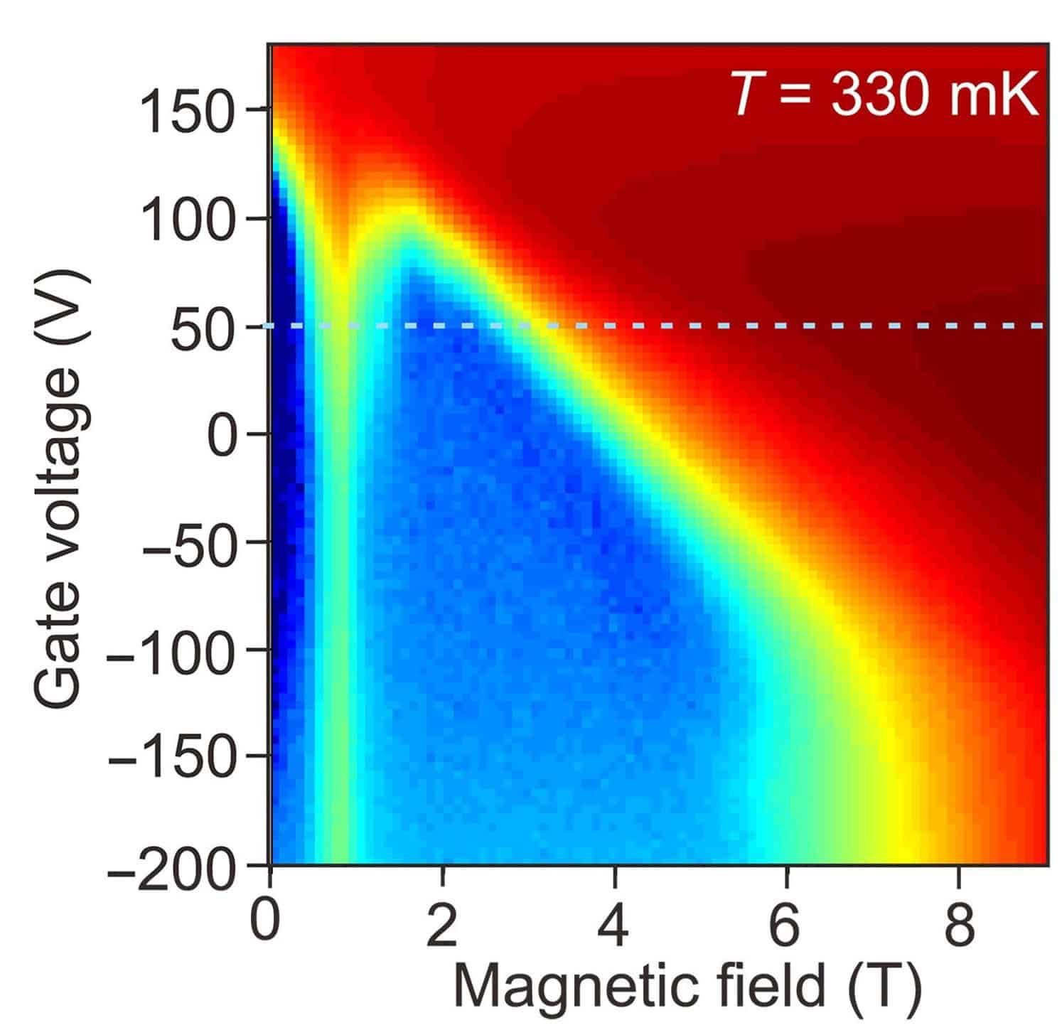
Writing in Science Advances, the physicists describe how they performed magnetotransport measurements on their LaTiO3/KTaO3 heterostructures to understand how these samples behaved in the presence of increasingly large applied magnetic fields. “We just wanted to see how the critical magnetic field behaves as a function of temperature, but suddenly we started seeing something else emerging at a rather low field: a resistive peak that seemed to separate two superconducting regions,” Maryenko says.

Rainbow colour plot of the interface resistance as a function of magnetic field and gate voltage. Higher gate voltages and magnetic fields are generally coloured red, but at a field of 0.9 T, there's a bright streak that appears to bleed down from the red area and stand out against the blue background.
Reentrant superconducting response: A plot of the interface resistance as a function of magnetic field and gate voltage, showing reentrant superconductivity at a magnetic field of around 0.9 T. (Courtesy: D Maryenko et al. Science Advances 12 26 DOI: 10.1126/sciadv.aeg0460)

This cusp, he explains, appears at a magnetic field B∗ of 0.9 T with zero resistance measured at both lower and higher applied fields. In this experiment, B∗ is independent of temperature and the concentration of charge carriers, which Maryenko and colleagues controlled experimentally by tuning a gate voltage across the interface.

Explaining re-entrant superconductivity

The researchers considered several possible explanations for the RSC, including Zeeman splitting, orbital effects and something called the Jaccarino-Peter effect, where internal and external magnetic fields compensate for each other and cancel out.

To identify the correct explanation, Igor Maznichenko and Sergey Ostanin from Martin Luther University in Germany and Arthur Ernst from Johannes Kepler University in Austria performed ab initio calculations to determine the electron band structure for the interface. These calculations identified the presence of a so-called Van Hove singularity, where for certain momenta, the electrons will have very high density of states.

Then, Vitalii Dugaev from Rzeszów University of Technology in Poland and Evgeny Ya Sherman at the University of the Basque Country in Spain developed a SOC-based model, taking inspiration from symmetry arguments and the ab initio band structure calculations. In the absence of an applied field, they found that there is a p ↔−p symmetry in the bands. This means that electrons with opposite momenta will have the same energy, so two electrons that form a Cooper pair, and have the same energy, have a total momentum equal to zero. In other words, the system favours spin-singlet Cooper pairs which form easily.

Applying a field breaks this symmetry, thereby reducing the Cooper pairing efficiency and decreasing the critical temperature Tc for the onset of superconductivity. On the other hand, the applied field also shifts the electrons closer towards the Van Hove singularity, increases the density of states and increases Tc. The combination of these opposing effects results in a minima appearing in Tc(B), hence RSC. The discovery of RSC in these materials establishes the system as a robust platform for studying unconventional superconductivity in 2D systems.

The post Magnetic field first kills superconductor, then brings it back to life appeared first on Physics World.

Advances in molecularly imprinted polymers for electrochemical sensing

21 August 2026 at 08:39

Molecularly imprinted polymers (MIPs) are synthetic receptors that can recognize target analytes through tailored binding sites, offering a stable, cost-effective and versatile alternative to natural bioreceptors. In electrochemical sensing, MIPs have attracted growing interest because they can provide high selectivity while enabling rapid, portable and low-cost detection.

This webinar will introduce the fundamentals of molecular imprinting, including binding site design, polymerization strategies, template removal and immobilization on electrode surfaces. It will then compare molecularly imprinted non-conducting polymers (MINPs) and molecularly imprinted conducting polymers (MICPs), focusing on their differences in conductivity, binding-site accessibility, reproducibility, sensitivity and selectivity. Recent advances in MIP-based electrochemical sensors will be discussed across representative applications, along with current limitations and design strategies to improve sensor performance.

The webinar will conclude with perspectives on how conducting polymers, nanomaterials and optimized molecular recognition can guide the development of next-generation selective and sensitive electrochemical sensors.

Wonhyeong Kim

Wonhyeong Kim is a postdoctoral research associate in the department of materials science and engineering at the University of Arizona. He received his PhD in materials engineering from Auburn University, where his research focused on molecularly imprinted polymers, conducting polymers and electrochemical sensors for selective chemical and biomarker detection. His work has resulted in multiple publications in leading journals and he was the recipient of the 2025 ECS Sensor Division Student Research Award for his contributions to molecularly imprinted polymer-based electrochemical sensors. His research interests include molecular imprinting, conducting polymers, electrochemical sensors and functional materials for selective chemical sensing, with recent work expanding into advanced polymeric materials and nanomaterials for environmental applications.


The post Advances in molecularly imprinted polymers for electrochemical sensing appeared first on Physics World.

Semiconducting nanorods help laser-powered drones keep cool

18 August 2026 at 16:43

Remote uncrewed aerial vehicles (UAVs), or drones, equipped with solar cells could be wirelessly charged using laser beams directed at them from the ground, rather than relying on traditional onboard batteries. The problem until now, however, has been keeping the drones cool – since laser light heats them up, so reducing the efficiency of the photovoltaic cells they carry on their wings. A team of researchers at the Civil Aviation University of China has now overcome this problem by incorporating a heat blocking technology based on antimony selenide (Sb2Se3) nanorods into these solar cells.

As drones take on longer missions, battery life has become one of the biggest barriers, explains Jianhua Han, who led this new research study. “Our team has been looking into laser wireless power transmission, which is a leading approach for long-distance wireless energy transfer, to replace these batteries.”

Laser wireless power transmission is particularly suited to aerospace applications such as UAVs equipped with photovoltaic cells. Perovskite solar cells show much promise in this context because they are cheap to manufacture, absorb light strongly in the visible part of the electromagnetic spectrum and have long charge-carrier diffusion lengths.

A perovskite laser cell-thermoelectric tandem device

In the new work, detailed in Matter & Light, Han and colleagues studied a type of solar cell known as a perovskite laser cell-thermoelectric (PLC-TE) tandem device, which consists of a carbon-based CsPbBr3 perovskite as the PLC and bismuth telluride (Bi2Te3) as the TE material. The TE module is directly fixed beneath the laser cell and a carbon electrode is attached to its negative terminal  to create a series connection. When laser light is shone onto the device, the carbon electrode converts a portion of the incident laser energy into heat. The TE then harvests this heat, converting it into electricity through the thermoelectric effect.

And that’s not all: since one side of the device ends up being warmer than the other, this temperature gradient also helps convert the thermal energy into electricity. The larger the temperature gradient, the more electricity the TE layer can generate.

There is a problem though: while the carbon in the hybrid structure dissipates some of the heat produced by the laser, the structure can still heat up – reaching temperatures of up to 90°C, says Han. “That was much higher than we expected and made us realize that heat buildup was a far more serious problem than we had imagined.”

Sb2Se3 behaves like a thermal barrier

To overcome this problem, the researchers turned to Sb2Se3, which is a promising photovoltaic material. As well as its good optoelectronic properties, this semiconductor also has a low thermal conductivity, which allows it to behave like a thermal barrier when embedded in a device.

Han’s team synthesized nanorods from the Sb2Se3 and incorporated them into the upper portion of the CsPbBr3 layer. The Sb2Se3 reduces heat dissipation in the carbon electrode and so helps maintain a significant temperature gradient in the TE device, thereby improving its overall energy conversion efficiency. Its thermal barrier properties also help decrease the PLC’s overall operating temperature during prolonged laser exposure.

The team then inserted the tandem device containing the Sb2Se3 nanorods beneath the wing of a stationary drone and carved out air channels through the wing to simulate real-world airflow conditions. When illuminated with high-power green laser light with a wavelength of 520 nm, they found that the device converted 38.49% of the incoming laser energy into electricity and successfully powered the drone’s propellor blade. This power conversion efficiency, says Han, is among the highest reported for this class of technology operating under similar conditions.

Device could help UAVs stay airborne for longer

“In terms of concept, this is the first time that a system-level scheme of the devices has been applied to a UAV power supply, expanding the work from pure materials research to application-oriented system design,” Han tells Physics World. “It demonstrates that powering UAVs with light is not just a theoretical concept, but an engineering pathway that can be practically implemented.”

The device could help UAVs stay airborne for longer, something that will be useful for applications like forest patrol, disaster monitoring and delivering packages, he says. But there is still much work to do before such applications become a reality. For one, the researchers will need to integrate the PLC-TE device into a lightweight drone for flight testing outdoors and to assess the safety of their technology. They will also need to find a way of accurately tracking moving drones with laser beams.

“Going from the ground-based proof stage to the real flight validation stage will require solving many engineering challenges,” says Han, “but our technology is a good starting point and verifying its viability is the core objective for the next phase in our study”.

The post Semiconducting nanorods help laser-powered drones keep cool appeared first on Physics World.

❌